Äîêóìåíòàöèÿ è îïèñàíèÿ www.docs.chipfind.ru
REV. A
Information furnished by Analog Devices is believed to be accurate and
reliable. However, no responsibility is assumed by Analog Devices for its
use, nor for any infringements of patents or other rights of third parties
which may result from its use. No license is granted by implication or
otherwise under any patent or patent rights of Analog Devices.
a
ADP3308
One Technology Way, P.O. Box 9106, Norwood, MA 02062-9106, U.S.A.
Tel: 781/329-4700
World Wide Web Site: http://www.analog.com
Fax: 781/326-8703
© Analog Devices, Inc., 1998
anyCAPTM 50 mA
Low Dropout Linear Regulator
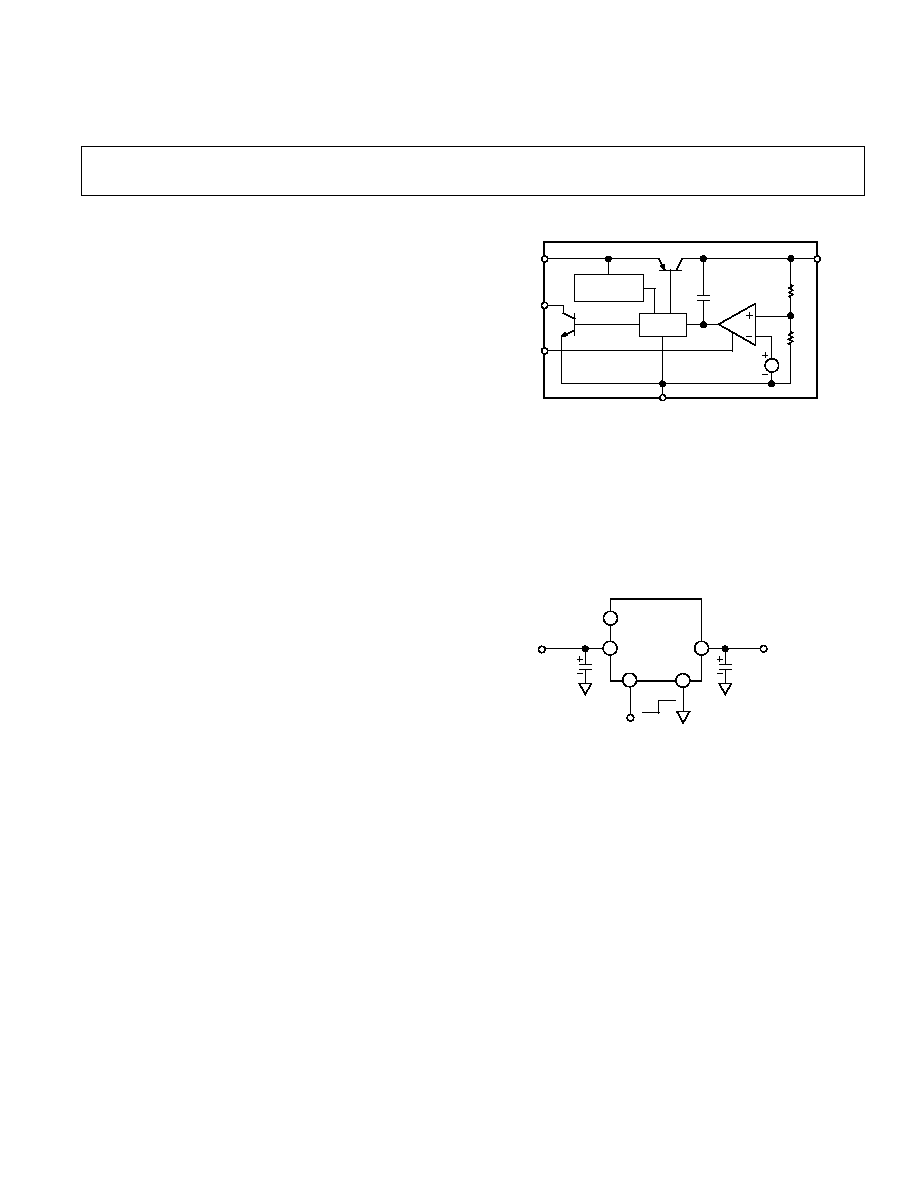
FUNCTIONAL BLOCK DIAGRAM
CC
OUT
GND
R1
R2
Q1
IN
SD
ADP3308
BANDGAP
REF
Q2
ERR
/NC
DRIVER
THERMAL
PROTECTION
Gm
FEATURES
1.2% Accuracy Over Line and Load Regulations
@ 25 C
Ultralow Dropout Voltage: 80 mV Typical @ 50 mA
Requires Only C
O
= 0.47 F for Stability
anyCAP = Stable with All Types of Capacitors
(Including MLCC)
Current and Thermal Limiting
Low Noise
Low Shutdown Current: 1 A
3.0 V to 12 V Supply Range
20 C to +85 C Ambient Temperature Range
Several Fixed Voltage Options
Ultrasmall SOT-23-5 Package
Excellent Line and Load Regulations
APPLICATIONS
Cellular Telephones
Notebook, Palmtop Computers
Battery Powered Systems
PCMCIA Regulator
Bar Code Scanners
Camcorders, Cameras
GENERAL DESCRIPTION
The ADP3308 is a member of the ADP330x family of precision
low dropout anyCAP voltage regulators. It is pin-for-pin and
functionally compatible with National's LP2980, but offers
performance advantages. The ADP3308 stands out from the
conventional LDOs with a novel architecture and an enhanced
process. Its patented design requires only a 0.47
µ
F output
capacitor for stability. This device is stable with any type of
capacitor regardless of its ESR (Equivalent Serial Resistance)
value, including ceramic types for space restricted applications.
The ADP3308 achieves
±
1.2% accuracy at room temperature
and
±
2.2% overall accuracy over temperature, line and load
regulations. The dropout voltage of the ADP3308 is only
80 mV (typical) at 50 mA. This device also includes a current
limit and a shutdown feature. In shutdown mode, the ground
current is reduced to ~1
µ
A.
The ADP3308 operates with a wide input voltage range from
3.0 V to 12 V and delivers a load current in excess of 100 mA.
The ADP3308 anyCAP LDO offers a wide range of output
voltages. For 100 mA version, refer to the ADP3309 data sheet.
anyCAP is a trademark of Analog Devices, Inc.
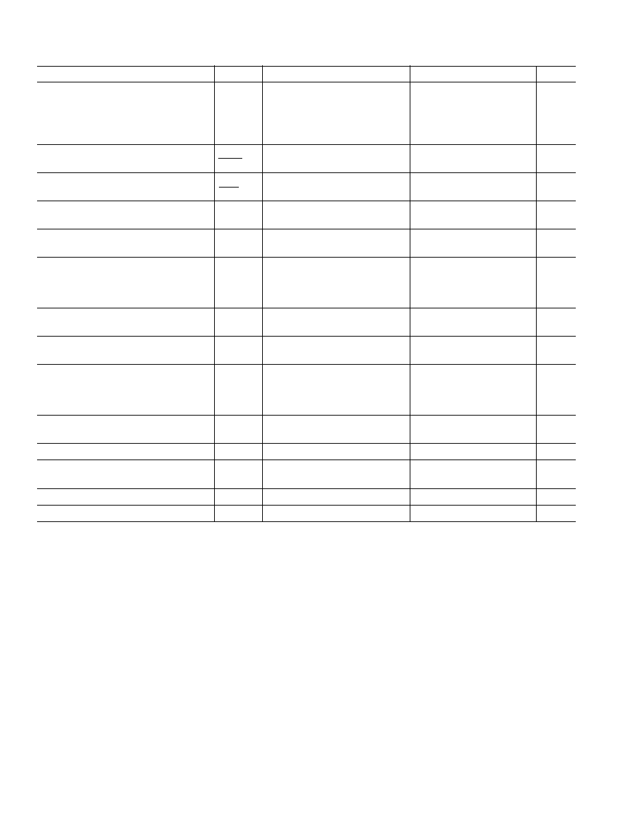
ADP3308-3.3
OUT
V
IN
IN
GND
V
OUT
= +3.3V
ON
OFF
5
SD
C1
0.47 F
C2
0.47 F
ERR
/NC
1
2
3
4
Figure 1. Typical Application Circuit
2
REV. A
ADP3308-xxSPECIFICATIONS
(@T
A
= 20 C to +85 C, V
IN
= 7 V, C
IN
= 0.47 F, C
OUT
= 0.47 F, unless
otherwise noted.)
1
The following specifications apply to all voltage options.
Parameter
Symbol
Conditions
Min
Typ
Max
Units
OUTPUT VOLTAGE ACCURACY
V
OUT
V
IN
= V
OUTNOM
+ 0.3 V to 12 V
I
L
= 0.1 mA to 50 mA
T
A
= +25
°
C
1.2
+1.2
%
V
IN
= V
OUTNOM
+ 0.3 V to 12 V
I
L
= 0.1 mA to 50 mA
2.2
+2.2
%
LINE REGULATION
V
IN
= V
OUTNOM
+ 0.3 V to 12 V
T
A
= +25
°
C
0.02
mV/V
LOAD REGULATION
I
L
= 0.1 mA to 50 mA
T
A
= +25
°
C
0.06
mV/mA
GROUND CURRENT
I
GND
I
L
= 50 mA
0.54
1.4
mA
I
L
= 0.1 mA
0.19
0.3
mA
GROUND CURRENT IN DROPOUT
I
GND
V
IN
= 2.4 V
I
L
= 0.1 mA
0.9
1.7
mA
DROPOUT VOLTAGE
V
DROP
V
OUT
= 98% of V
OUTNOM
I
L
= 50 mA
0.08
0.17
V
I
L
= 10 mA
0.025
0.07
V
I
L
= 1 mA
0.004
0.030
V
SHUTDOWN THRESHOLD
V
THSD
ON
2.0
0.75
V
OFF
0.75
0.3
V
SHUTDOWN PIN INPUT CURRENT
I
SDIN
0 < V
SD
5 V
1
µ
A
5 < V
SD
12 V @ V
IN
= 12 V
9
µ
A
GROUND CURRENT IN SHUTDOWN
I
Q
V
SD
= 0 V, V
IN
= 12 V
MODE
T
A
= +25
°
C
0.005
1
µ
A
V
SD
= 0 V, V
IN
= 12 V
T
A
= +85
°
C
0.01
3
µ
A
OUTPUT CURRENT IN SHUTDOWN
I
OSD
T
A
= +25
°
C @ V
IN
= 12 V
2
µ
A
MODE
T
A
= +85
°
C @ V
IN
= 12 V
4
µ
A
ERROR PIN OUTPUT LEAKAGE
I
EL
13
µ
A
ERROR PIN OUTPUT
"LOW" VOLTAGE
V
EOL
I
SINK
= 400
µ
A
0.12
0.3
V
PEAK LOAD CURRENT
I
LDPK
V
IN
= V
OUTNOM
+ 1 V, T
A
= +25
°
C
150
mA
OUTPUT NOISE @ 5 V OUTPUT
V
NOISE
f = 10 Hz100 kHz
100
µ
V
rms
NOTES
1
Ambient temperature of +85
°
C corresponds to a junction temperature of +125
°
C under typical full load test conditions.
Specifications subject to change without notice.
V
O
V
IN
V
O
I
L
ADP3308
3
REV. A
ABSOLUTE MAXIMUM RATINGS*
Input Supply Voltage . . . . . . . . . . . . . . . . . . . 0.3 V to +16 V
Shutdown Input Voltage . . . . . . . . . . . . . . . . 0.3 V to +16 V
Power Dissipation . . . . . . . . . . . . . . . . . . . . Internally Limited
Operating Ambient Temperature Range . . . 55
°
C to +125
°
C
Operating Junction Temperature Range . . . 55
°
C to +125
°
C
JA
. . . . . . . . . . . . . . . . . . . . . . . . . . . . . . . . . . . . 165
°
C/W
JC
. . . . . . . . . . . . . . . . . . . . . . . . . . . . . . . . . . . . . 92
°
C/W
Storage Temperature Range . . . . . . . . . . . . 65
°
C to +150
°
C
Lead Temperature Range (Soldering 10 sec) . . . . . . . . +300
°
C
Vapor Phase (60 sec) . . . . . . . . . . . . . . . . . . . . . . . . +215
°
C
Infrared (15 sec) . . . . . . . . . . . . . . . . . . . . . . . . . . . . +220
°
C
*This is a stress rating only; operation beyond these limits can cause the device to
be permanently damaged.
ORDERING GUIDE
Voltage
Package
Marking
Model
Output
Option*
Code
ADP3308ART-2.7
2.7 V
SOT-23
DAC
ADP3308ART-2.85
2.85 V
SOT-23
DJC
ADP3308ART-2.9
2.9 V
SOT-23
DKC
ADP3308ART-3
3.0 V
SOT-23
DCC
ADP3308ART-3.3
3.3 V
SOT-23
DEC
ADP3308ART-3.6
3.6 V
SOT-23
DFC
*SOT = Surface Mount.
Contact the factory for the availability of other output voltage options.
Other Member of anyCAP Family
1
Model
Output Current
Package Option
2
ADP3309
100 mA
SOT-23-5 Lead
NOTES
1
See individual data sheet for detailed ordering information.
2
SOT = Surface Mount.
PIN FUNCTION DESCRIPTIONS
Pin Name
Function
1
IN
Regulator Input.
2
GND
Ground Pin.
3
SD
Active Low Shutdown Pin. Connect to
ground to disable the regulator output.
When shutdown is not used, this pin
should be connected to the input pin.
4
ERR/NC Open Collector. Output that goes low
to indicate the output is about to go out
of regulation or no connect.
5
OUT
Output of the Regulator, fixed 2.7, 2.85,
2.9, 3.0, 3.3, or 3.6 volts output voltage.
Bypass to ground with a 0.47
µ
F or larger
capacitor.
PIN CONFIGURATION
1
2
3
4
5
TOP VIEW
(Not to Scale)
IN
GND
OUT
ADP3308
SD
ERR
/NC
NC = NO CONNECT
CAUTION
ESD (electrostatic discharge) sensitive device. Electrostatic charges as high as 4000 V readily
accumulate on the human body and test equipment and can discharge without detection.
Although the ADP3308 features proprietary ESD protection circuitry, permanent damage may
occur on devices subjected to high energy electrostatic discharges. Therefore, proper ESD
precautions are recommended to avoid performance degradation or loss of functionality.
WARNING!
ESD SENSITIVE DEVICE
ADP3308
4
REV. A
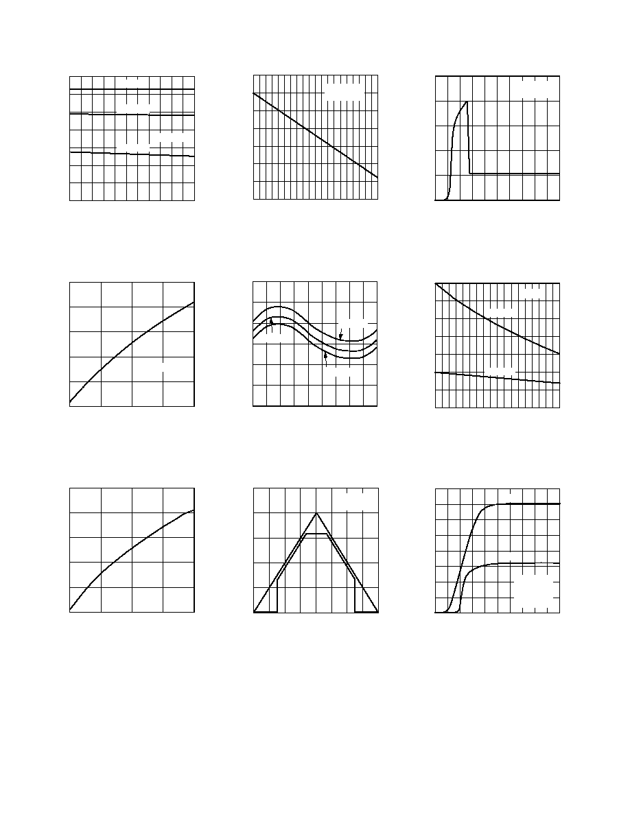
Typical Performance Characteristics
INPUT VOLTAGE Volts
OUTPUT VOLTAGE Volts
3.302
3.299
3.296
3.3
14
4
5
6
7
8
9
10 11 12 13
3.301
3.300
3.298
3.297
I
L
= 0mA
I
L
= 10mA
I
L
= 50mA
V
OUT
= 3.3V
3.295
Figure 2. Line Regulation: Output
Voltage vs. Supply Voltage
OUTPUT LOAD mA
800
GROUND CURRENT
A 675
175
0
80
20
40
60
550
425
300
I
L
= 0 TO 80mA
Figure 5. Quiescent Current vs. Load
Current
OUTPUT LOAD mA
120
96
0
80
20
40
60
72
48
24
0
INPUT/OUTPUT VOLTAGE mV
Figure 8. Dropout Voltage vs. Output
Current
OUTPUT VOLTAGE Volts
OUTPUT LOAD mA
3.302
3.295
0
80
8
16
24 32 40
48
56 64 72
3.301
3.300
3.299
3.298
3.297
3.296
V
OUT
= 3.3V
V
IN
= 7V
Figure 3. Output Voltage vs. Load
Current
TEMPERATURE C
OUTPUT VOLTAGE %
0.2
0.4
45 25
135
5
15
35
75
95 115
55
0.1
0.0
0.1
0.2
0.3
I
L
= 0mA
I
L
= 30mA
I
L
= 50mA
Figure 6. Output Voltage Variation %
vs. Temperature
INPUT VOLTAGE Volts
5
0
0
3
0
4
3
2
4
2
1
3
2
1
1
INPUT/OUTPUT VOLTAGE Volts
V
OUT
= 3.3V
R
L
= 66
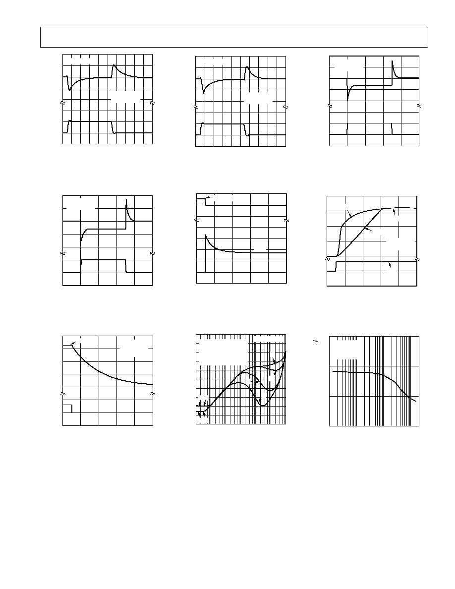
Figure 9. Power-Up/Power-Down
INPUT VOLTAGE Volts
1150
900
0
0
12.0
1.2 2.4 3.6 4.8 6.0 7.2 8.4 9.6 10.8
650
400
GROUND CURRENT
A
160
V
OUT
= 3.3V
I
L
= 0mA
Figure 4. Quiescent Current vs.
Supply Voltage
TEMPERATURE C
700
0
45 25
600
400
300
200
100
500
15
35
55
75
95 115 135
5
V
IN
= 7V
GROUND CURRENT
A
I
L
= 50mA
I
L
= 0mA
Figure 7. Quiescent Current vs.
Temperature
TIME s
0
0
100
200
2.0
V
SD
= V
IN
C
L
= 0.47 F
R
L
= 66
V
OUT
= 3.3V
1.0
3.0
4.0
5.0
6.0
7.0
8.0
20
INPUT/OUTPUT VOLTAGE Volts
40 60 80
120 140 160 180
V
IN
V
OUT
Figure 10. Power-Up Overshoot
ADP3308
5
REV. A
TIME s
Volts
3.320
3.280
0
400
40 80 120 160 200 240 280 320 360
3.310
3.300
7.5
7.0
3.290
R
L
= 66
C
L
= 0.47 F
V
IN
V
OUT
= 3.3V
Figure 11. Line Transient Response
TIME s
Volts
3.320
3.290
0
500
100
200
300
400
3.310
100
10
3.300
V
OUT
= 3.3V
C
L
= 4.7 F
mA
3.280
I
OUT
Figure 14. Load Transient
TIME s
2
0
0
100
20
40
60
80
1
0
4
3
3
V
OUT
= 3.3V
R
L
= 66
C
L
= 0.47 F
Volts
3.3V
V
SD
Figure 17. Turn Off
TIME s
Volts
3.320
3.280
0
200
20
40 60
80 100 120 140 160 180
3.310
3.300
7.5
7.0
3.290
R
L
= 3.3k
C
L
= 0.47 F
V
OUT
= 3.3V
V
IN
Figure 12. Line Transient Response
TIME s
200
0
0
5
1
2
3
4
150
100
3.3
0
50
mA
I
OUT
V
OUT
= 3.3V
Volts
V
OUT
Figure 15. Short Circuit Current
FREQUENCY Hz
RIPPLE REJECTION dB
0
100
10
100
10M
1k
10k
100k
1M
10
60
70
80
90
20
30
50
40
b d
a c
b
d
a
c
V
OUT
= +3.3V
a. 0.47 F, R
L
= 3.3k
b. 0.47 F, R
L
= 66
c. 4.7 F, R
L
= 3.3k
d. 4.7 F, R
L
= 66
Figure 18. Power Supply Ripple
Rejection
TIME s
3.320
3.280
0
500
100
200
300
400
3.310
3.300
100
10
3.290
V
OUT
= 3.3V
C
L
= 0.47 F
Volts
mA
I
OUT
Figure 13. Load Transient
TIME s
2
0
0
100
20
40
60
80
1
0
4
3
+3
V
OUT
= 3.3V
R
L
= 66
Volts
V
OUT
C
L
= 0.47 F
3.3V
C
L
= 4.7 F
V
SD
+3V
Figure 16. Turn On
FREQUENCY Hz
VOLTAGE NOISE SPECTRAL DENSITY
V/
Hz
10
1
0.01
100
1k
100k
10k
0.1
V
OUT
= 3.3V
C
L
= 0.47 F
I
L
= 1mA
Figure 19. Output Noise Density