Äîêóìåíòàöèÿ è îïèñàíèÿ www.docs.chipfind.ru
REV. 0
Information furnished by Analog Devices is believed to be accurate and
reliable. However, no responsibility is assumed by Analog Devices for its
use, nor for any infringements of patents or other rights of third parties
which may result from its use. No license is granted by implication or
otherwise under any patent or patent rights of Analog Devices.
a
ADP3309
One Technology Way, P.O. Box 9106, Norwood, MA 02062-9106, U.S.A.
Tel: 781/329-4700
World Wide Web Site: http://www.analog.com
Fax: 781/326-8703
© Analog Devices, Inc., 1998
anyCAPTM 100 mA
Low Dropout Linear Regulator
FUNCTIONAL BLOCK DIAGRAM
THERMAL
PROTECTION
DRIVER
G
M
CC
IN
ADP3309
OUT
R1
R2
GND
Q1
ERR/
NC
SD
BANDGAP
REF
Q2
FEATURES
1.2% Accuracy Over Line and Load Regulations @ +25 C
Ultralow Dropout Voltage: 120 mV Typical @ 100 mA
Requires Only C
O
= 0.47 F for Stability
anyCAP = Stable with All Types of Capacitors
(Including MLCC)
Current and Thermal Limiting
Low Noise
Low Shutdown Current: 1 A
3.0 V to 12 V Supply Range
20 C to +85 C Ambient Temperature Range
Several Fixed Voltage Options
Ultrasmall SOT-23-5 Package
Excellent Line and Load Regulations
APPLICATIONS
Cellular Telephones
Notebook, Palmtop Computers
Battery Powered Systems
PCMCIA Regulator
Bar Code Scanners
Camcorders, Cameras
GENERAL DESCRIPTION
The ADP3309 is a member of the ADP330x family of precision
low dropout anyCAP voltage regulators. It is pin-for-pin and
functionally compatible with National's LP2981, but offers
performance advantages. The ADP3309 stands out from con-
ventional LDOs with a novel architecture and an enhanced
process. Its patented design requires only a 0.47
µ
F output
capacitor for stability. This device is stable with any type of
capacitor regardless of its ESR (Equivalent Series Resistance)
value, including ceramic types for space restricted applications.
The ADP3309 achieves
±
1.2% accuracy at room temperature
and
±
2.2% overall accuracy over temperature, line and load
regulations. The dropout voltage of the ADP3309 is only
120 mV (typical) at 100 mA. This device also includes a current
limit and a shutdown feature. In shutdown mode, the ground
current is reduced to ~1
µ
A.
The ADP3309 operates with a wide input voltage range from
3.0 V to 12 V and delivers a load current in excess of 100 mA.
The ADP3309 anyCAP LDO offers a wide range of output
voltages. For a 50 mA version, refer to the ADP3308 data sheet.
V
OUT
= +3.3V
V
IN
+
ADP3309-3.3
OUT
ERR/
NC
ON
OFF
SD
GND
IN
C2
0.47 F
C1
0.47 F
+
Figure 1. Typical Application Circuit
anyCAP is a trademark of Analog Devices, Inc.
2
REV. 0
ADP3309-xxSPECIFICATIONS
Parameter
Symbol
Conditions
Min
Typ
Max
Units
OUTPUT VOLTAGE ACCURACY
V
OUT
V
IN
= V
OUTNOM
+ 0.3 V to 12 V
I
L
= 0.1 mA to 100 mA
T
A
= +25
°
C
1.2
+1.2
%
V
IN
= V
OUTNOM
+ 0.3 V to 12 V
I
L
= 0.1 mA to 100 mA
2.2
+2.2
%
LINE REGULATION
V
IN
= V
OUTNOM
+ 0.3 V to 12 V
T
A
= +25
°
C
0.02
mV/V
LOAD REGULATION
I
L
= 0.1 mA to 100 mA
T
A
= +25
°
C
0.06
mV/mA
GROUND CURRENT
I
GND
I
L
= 100 mA
0.8
2.0
mA
I
L
= 0.1 mA
0.19
0.3
mA
GROUND CURRENT IN DROPOUT
I
GND
V
IN
= 2.4 V
I
L
= 0.1 mA
0.9
1.7
mA
DROPOUT VOLTAGE
V
DROP
V
OUT
= 98% of V
OUTNOM
I
L
= 100 mA
0.12
0.25
V
I
L
= 10 mA
0.025
0.07
V
I
L
= 1 mA
0.004
0.015
V
SHUTDOWN THRESHOLD
V
THSD
ON
2.0
0.75
V
OFF
0.75
0.3
V
SHUTDOWN PIN INPUT CURRENT
I
SDIN
0 < V
SD
5 V
1
µ
A
5 < V
SD
12 V @ V
IN
= 12 V
9
µ
A
GROUND CURRENT IN SHUTDOWN
I
Q
V
SD
= 0 V, V
IN
= 12 V
MODE
T
A
= +25
°
C
0.005
1
µ
A
V
SD
= 0 V, V
IN
= 12 V
T
A
= +85
°
C
0.01
3
µ
A
OUTPUT CURRENT IN SHUTDOWN
I
OSD
T
A
= +25
°
C @ V
IN
= 12 V
2
µ
A
MODE
T
A
= +85
°
C @ V
IN
= 12 V
4
µ
A
ERROR PIN OUTPUT LEAKAGE
I
EL
V
EO
= 5 V
13
µ
A
ERROR PIN OUTPUT
"LOW" VOLTAGE
V
EOL
I
SINK
= 400
µ
A
0.12
0.3
V
PEAK LOAD CURRENT
I
LDPK
V
IN
= V
OUTNOM
+ 1 V, T
A
= +25
°
C
150
mA
OUTPUT NOISE @ 5 V OUTPUT
V
NOISE
f = 10 Hz100 kHz
100
µ
V
rms
NOTES
1
Ambient temperature of +85
°
C corresponds to a junction temperature of 125
°
C under typical full load test conditions.
Specifications subject to change without notice.
(@T
A
= 20 C to +85 C, V
IN
= 7 V, C
IN
= 0.47 F, C
OUT
= 0.47 F, unless
otherwise noted.)
1
The following specifications apply to all voltage options.
V
O
V
IN
V
O
I
L
ADP3309
3
REV. 0
ABSOLUTE MAXIMUM RATINGS*
Input Supply Voltage . . . . . . . . . . . . . . . . . . . 0.3 V to +16 V
Shutdown Input Voltage . . . . . . . . . . . . . . . . 0.3 V to +16 V
Power Dissipation . . . . . . . . . . . . . . . . . . . . Internally Limited
Operating Ambient Temperature Range . . . 55
°
C to +125
°
C
Operating Junction Temperature Range . . . 55
°
C to +125
°
C
JA
. . . . . . . . . . . . . . . . . . . . . . . . . . . . . . . . . . . . 190
°
C/W
JC
. . . . . . . . . . . . . . . . . . . . . . . . . . . . . . . . . . . . . 92
°
C/W
Storage Temperature Range . . . . . . . . . . . . 65
°
C to +150
°
C
Lead Temperature Range (Soldering 10 sec) . . . . . . . . +300
°
C
Vapor Phase (60 sec) . . . . . . . . . . . . . . . . . . . . . . . . +215
°
C
Infrared (15 sec) . . . . . . . . . . . . . . . . . . . . . . . . . . . . +220
°
C
*This is a stress rating only; operation beyond these limits can cause the device to
be permanently damaged.
ORDERING GUIDE
Voltage
Package
Marking
Model
Output
Option*
Code
ADP3309ART-2.7
2.7 V
SOT-23
DNC
ADP3309ART-2.85
2.85 V
SOT-23
DVC
ADP3309ART-2.9
2.9 V
SOT-23
DWC
ADP3309ART-3
3.0 V
SOT-23
DPC
ADP3309ART-3.3
3.3 V
SOT-23
DRC
ADP3309ART-3.6
3.6 V
SOT-23
DSC
*SOT = Surface Mount.
Contact the factory for the availability of other output voltage options.
Other Member of anyCAP Family
1
Model
Output Current
Package Option
2
ADP3308
50 mA
SOT-23-5 Lead
NOTES
1
See individual data sheet for detailed ordering information.
2
SOT = Surface Mount.
PIN FUNCTION DESCRIPTIONS
Pin Name
Function
1
IN
Regulator Input.
2
GND
Ground Pin.
3
SD
Active Low Shutdown Pin. Connect to
ground to disable the regulator output.
When shutdown is not used, this pin
should be connected to the input pin.
4
ERR/NC Open Collector. Output that goes low
to indicate the output is about to go
out of regulation. This pin can be left open.
(NC = No Connect).
5
OUT
Output of the Regulator, fixed 2.7, 2.85,
2.9, 3.0, 3.3 or 3.6 volts output voltage.
Bypass to ground with a 0.47
µ
F or larger
capacitor.
PIN CONFIGURATION
GND
TOP VIEW
(Not to Scale)
SD
OUT
ADP3309
IN
ERR/
NC
NC = NO CONNECT
CAUTION
ESD (electrostatic discharge) sensitive device. Electrostatic charges as high as 4000 V readily
accumulate on the human body and test equipment and can discharge without detection.
Although the ADP3309 features proprietary ESD protection circuitry, permanent damage may
occur on devices subjected to high energy electrostatic discharges. Therefore, proper ESD
precautions are recommended to avoid performance degradation or loss of functionality.
WARNING!
ESD SENSITIVE DEVICE
ADP3309
4
REV. 0
Typical Performance Characteristics
INPUT VOLTAGE Volts
OUTPUT VOLTAGE Volts
3.302
3.298
3.295
3.3
4
14
5
6
7
8
9
10 11 12 13
3.301
3.300
3.297
3.296
3.299
V
OUT
= +3.3V
I
L
= 0mA
I
L
= 10mA
I
L
= 100mA
I
L
= 50mA
Figure 2. Line Regulation: Output
Voltage vs. Supply Voltage
OUTPUT LOAD mA
GROUND CURRENT
A
900
750
150
0
25
100
50
75
600
450
300
I
L
= 0 TO 100mA
Figure 5. Quiescent Current vs. Load
Current
OUTPUT LOAD mA
INPUT-OUTPUT VOLTAGE mV
120
96
0
0
25
100
50
75
72
48
24
Figure 8. Dropout Voltage vs. Output
Current
OUTPUT LOAD mA
OUTPUT VOLTAGE Volts
3.302
3.295
0
10
100
20
30
40 50
60
70
80
90
3.301
3.300
3.299
3.298
3.297
3.296
V
OUT
= +3.3V
V
IN
= +7V
Figure 3. Output Voltage vs. Load
Current
0.2
0.4
45 25
135
5
15
35
75
95 115
55
0.1
0.0
0.1
0.2
0.3
I
L
= 50mA
I
L
= 100mA
TEMPERATURE C
OUTPUT VOLTAGE %
I
L
= 0mA
Figure 6. Output Voltage Variation %
vs. Temperature
5
4
0
0
1
0
2
3
4
3
2
1
3
2
1
V
OUT
= +3.3V
R
L
= 33
INPUT/OUTPUT VOLTAGE Volts
INPUT VOLTAGE Volts
Figure 9. Power-Up/Power-Down
INPUT VOLTAGE Volts
GROUND CURRENT
A
1150
900
0
0
1.2
12.0
2.4 3.6 4.8 6.0 7.2 8.4 9.6 10.8
650
400
160
V
OUT
= +3.3V
I
L
= 0mA
Figure 4. Quiescent Current vs.
Supply Voltage
TEMPERATURE C
GROUND CURRENT
A
1250
1000
0
25
5
135
15
35
55
75
95
115
750
500
250
I
L
= 0mA
V
IN
= +7V
I
L
= 100mA
Figure 7. Quiescent Current vs.
Temperature
TIME s
INPUT/OUTPUT VOLTAGE Volts
8.0
5.0
0
0
20
200
40
60
80 100 120 140 160 180
7.0
6.0
3.0
1.0
4.0
2.0
V
SD
= V
IN
C
L
= 0.47 F
R
L
= 33
V
OUT
= +3.3V
V
IN
V
OUT
Figure 10. Power-Up Overshoot
ADP3309
5
REV. 0
Volts
3.320
3.290
0
40
400
80 120 160 200 240 280 320 360
3.310
3.300
7.0
3.280
7.5
V
OUT
= +3.3V
R
L
= 33
C
L
= 0.47 F
V
IN
TIME s
Figure 11. Line Transient Response
3.320
3.310
0
100
500
200
300
400
3.290
3.280
100
10
3.300
Volts
mA
TIME s
V
OUT
= +3.3V
C
L
= 4.7 F
I
OUT
µ
Figure 14. Load Transient
Volts
4
3
0
10
50
20
30
40
1
0
3
0
2
TIME s
V
SD
V
OUT
= +3.3V
R
L
= 33
C
L
= 0.47 F
+3.3V
Figure 17. Turn Off
TIME s
Volts
3.320
3.290
0
20
200
40
60
80 100 120 140 160 180
3.310
3.300
7.0
3.280
7.5
V
OUT
= +3.3V
R
L
= 3.3k
C
L
= 0.47 F
V
IN
Figure 12. Line Transient Response
V
OUT
= +3.3V
mA
300
200
0
1
5
2
3
4
0
4
2
0
100
Volts
V
OUT
I
OUT
TIME sec
0.5
4.5
1.5
2.5
3.5
Figure 15. Short Circuit Current
FREQUENCY Hz
RIPPLE REJECTION dB
10
100
10M
1k
10k
1M
0
10
100
20
30
40
50
60
70
100k
a. 0.47 F, R
L
= 33k
b. 0.47 F, R
L
= 33
c. 10 F, R
L
= 33k
d. 10 F, R
L
= 33
V
OUT
= +3.3V
d
c
b
a
80
90
d
b
c
a
Figure 18. Power Supply Ripple
Rejection
3.320
3.310
0
100
500
200
300
400
3.290
3.280
100
10
3.300
Volts
mA
TIME s
V
OUT
= +3.3V
C
L
= 0.47 F
I
OUT
Figure 13. Load Transient
Volts
4
3
0
0
20
100
40
60
80
2
1
0
3
V
SD
C
L
= 0.47 F
V
OUT
+3.3V
C
L
= 4.7 F
V
OUT
= +3.3V
R
L
= 33
+3V
TIME s
Figure 16. Turn On
10
1
0.01
100
1k
100k
10k
0.1
FREQUENCY Hz
VOLTAGE NOISE SPECTRAL DENSITY
V Hz
V
OUT
= +3.3V, C
L
= 0.47 F
I
L
= 1mA
Figure 19. Output Noise Density
ADP3309
6
REV. 0
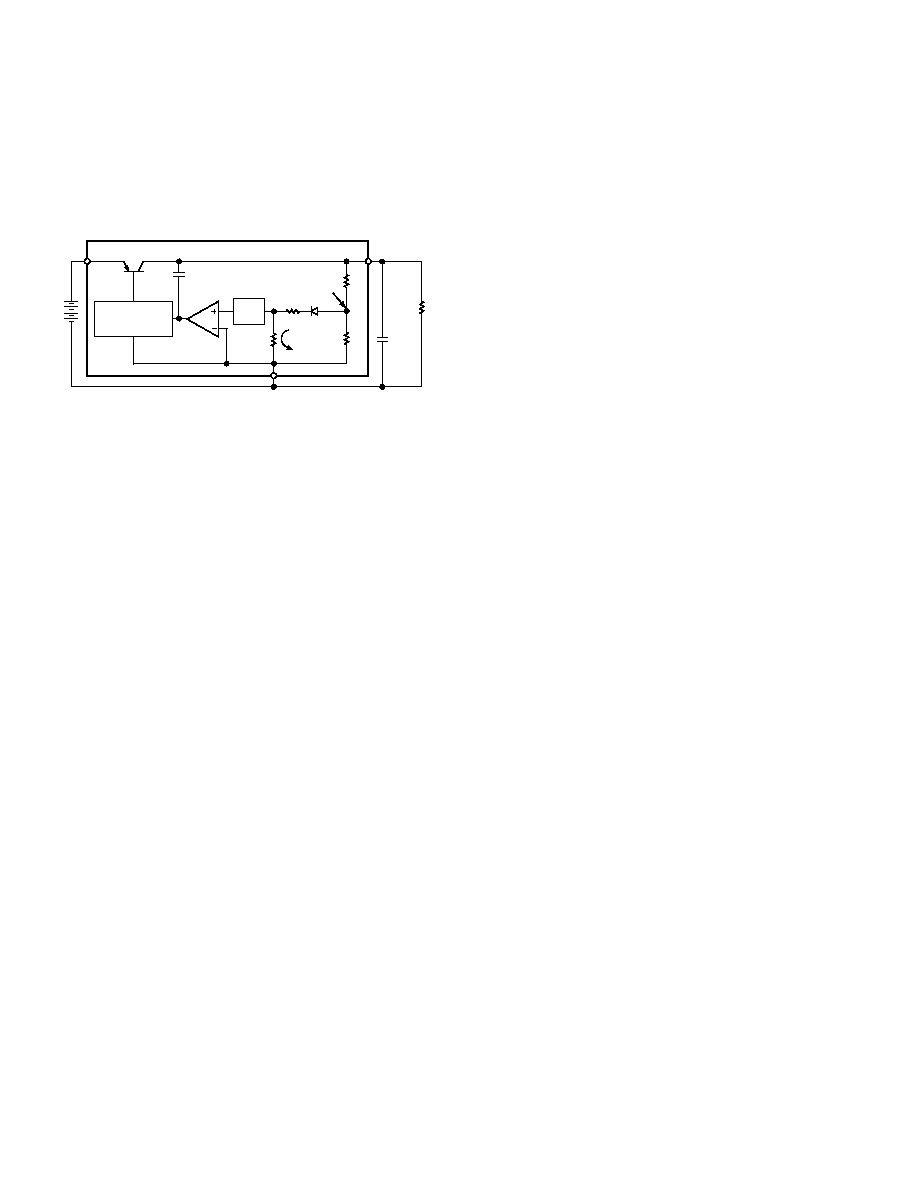
THEORY OF OPERATION
The ADP3309 anyCAP LDO uses a single control loop for
regulation and reference functions. The output voltage is sensed
by a resistive voltage divider consisting of R1 and R2, which is
varied to provide the available output voltage option. Feedback
is taken from this network by way of a series diode (D1) and a
second resistor divider (R3 and R4) to the input of an amplifier.
G
M
PTAT
V
OS
NONINVERTING
WIDEBAND
DRIVER
INPUT
Q1
ADP3309
COMPENSATION
CAPACITOR
ATTENUATION
(V
BANDGAP
/V
OUT
)
R1
D1
R2
OUTPUT
PTAT
CURRENT
R
LOAD
C
LOAD
(a)
GND
R4
R3
Figure 20. Functional Block Diagram
A very high gain error amplifier is used to control this loop. The
amplifier is constructed in such a way that at equilibrium it
produces a large, temperature proportional input "offset volt-
age" that is repeatable and very well controlled. The tem-
perature proportional offset voltage is combined with the
complementary diode voltage to form a "virtual bandgap" volt-
age, implicit in the network, although it never appears explicitly
in the circuit. Ultimately, this patented design makes it possible
to control the loop with only one amplifier. This technique also
improves the noise characteristics of the amplifier by providing
more flexibility on the trade-off of noise sources that leads to a
low noise design.
The R1, R2 divider is chosen in the same ratio as the bandgap
voltage to the output voltage. Although the R1, R2 resistor
divider is loaded by the diode D1, and a second divider consist-
ing of R3 and R4, the values can be chosen to produce a tem-
perature stable output.
The patented amplifier controls a new and unique noninverting
driver that drives the pass transistor, Q1. The use of this special
noninverting driver enables the frequency compensation to
include the load capacitor in a pole splitting arrangement to
achieve reduced sensitivity to the value, type and ESR of the
load capacitance.
Most LDOs place very strict requirements on the range of ESR
values for the output capacitor because they are difficult to
stabilize due to the uncertainty of load capacitance and resis-
tance. Moreover, the ESR value, required to keep conventional
LDOs stable, changes depending on load and temperature.
These ESR limitations make designing with LDOs more diffi-
cult because of their unclear specifications and extreme varia-
tions over temperature.
This is no longer true with the ADP3309 anyCAP LDO. It can
be used with virtually any capacitor, with no constraint on the
minimum ESR. This innovative design allows the circuit to be
stable with just a small 0.47
µ
F capacitor on the output. Addi-
tional advantages of the design scheme include superior line
noise rejection and very high regulator gain which leads to ex-
cellent line and load regulation. An impressive
±
2.2% accuracy
is guaranteed over line, load and temperature.
Additional features of the circuit include current limit and ther-
mal shutdown. Compared to the standard solutions that give
warning after the output has lost regulation, the ADP3309
provides improved system performance by enabling the
ERR
pin to give warning before the device loses regulation.
As the chip's temperature rises above 165
°
C, the circuit acti-
vates a soft thermal shutdown, indicated by a signal low on the
ERR pin, to reduce the current to a safe level.
APPLICATION INFORMATION
Capacitor Selection: anyCAP
Output Capacitors: As with any micropower device, output
transient response is a function of the output capacitance. The
ADP3309 is stable with a wide range of capacitor values, types
and ESR (anyCAP). A capacitor as low as 0.47
µ
F is all that is
needed for stability. However, larger capacitors can be used if
high output current surges are anticipated. The ADP3309 is
stable with extremely low ESR capacitors (ESR
0), such as
multilayer ceramic capacitors (MLCC) or OSCON.
Input Bypass Capacitor: An input bypass capacitor is not re-
quired. However, for applications where the input source is high
impedance or far from the input pin, a bypass capacitor is rec-
ommended. Connecting a 0.47
µ
F capacitor from the input pin
(Pin 1) to ground reduces the circuit's sensitivity to PC board
layout. If a bigger output capacitor is used, the input capacitor
must be 1
µ
F minimum.
Thermal Overload Protection
The ADP3309 is protected against damage due to excessive
power dissipation by its thermal overload protection circuit,
which limits the die temperature to a maximum of 165
°
C.
Under extreme conditions (i.e., high ambient temperature and
power dissipation) where die temperature starts to rise above
165
°
C, the output current is reduced until the die temperature
has dropped to a safe level. The output current is restored when
the die temperature is reduced.
Current and thermal limit protections are intended to protect
the device against accidental overload conditions. For normal
operation, device power dissipation should be externally limited
so that junction temperatures will not exceed 125
°
C.
Calculating Junction Temperature
Device power dissipation is calculated as follows:
P
D
= (V
IN
V
OUT
) I
LOAD
+ (V
IN
) I
GND
Where I
LOAD
and I
GND
are load current and ground current, V
IN
and V
OUT
are input and output voltages respectively.
Assuming I
LOAD
= 100 mA, I
GND
= 2 mA, V
IN
= 5.0 V and
V
OUT
= 3.3 V, device power dissipation is:
P
D
= (5.0 3.3) 100 mA + 5.0
×
2 mA = 180 mW
T = T
J
T
A
= P
D
×
JA
= 0.18
×
190 = 34.2
°
C
With a maximum junction temperature of 125
°
C, this yields a
maximum ambient temperature of ~90
°
C.
Printed Circuit Board Layout Consideration
Surface mount components rely on the conductive traces or
pads to transfer heat away from the device. Appropriate PC
board layout techniques should be used to remove heat from the
immediate vicinity of the package.
ADP3309
7
REV. 0
The following general guidelines will be helpful when designing
a board layout:
1. PC board traces with larger cross section areas will remove
more heat. For optimum results, use PC boards with thicker
copper and or wider traces.
2. Increase the surface area exposed to open air so heat can be
removed by convection or forced air flow.
3. Do not use solder mask or silk screen on the heat dissipating
traces because it will increase the junction to ambient
thermal resistance of the package.
Shutdown Mode
Applying a TTL high signal to the shutdown pin or tying it to
the input pin will turn the output ON. Pulling the shutdown pin
down to a TTL low signal or tying it to ground will turn the
output OFF. In shutdown mode, quiescent current is reduced
to less than 1
µ
A.
Error Flag Dropout Detector
The ADP3309 will maintain its output voltage over a wide
range of load, input voltage and temperature conditions. If the
output is about to lose regulation, for example, by reducing the
supply voltage below the combined regulated output and drop-
out voltages, the
ERR pin will be activated. The ERR output is
an open collector that will be driven low.
Once set, the
ERRor flag's hysteresis will keep the output low
until a small margin of operating range is restored either by
raising the supply voltage or reducing the load.
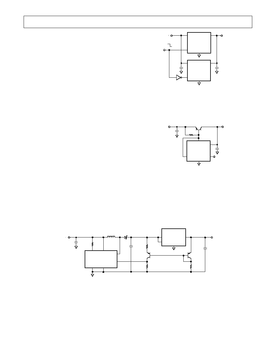
APPLICATION CIRCUITS
Crossover Switch
The circuit in Figure 21 shows that two ADP3309s can be used
to form a mixed supply voltage system. The output switches
between two different levels selected by an external digital input.
Output voltages can be any combination of voltages from the
Ordering Guide of the data sheet.
V
OUT
= 2.7V/3.3V
V
IN
= 4V TO 12V
OUTPUT SELECT
4V
0V
ADP3309-2.7
OUT
IN
SD
GND
ADP3309-3.3
+
+
IN
OUT
C1
1.0 F
C2
0.47 F
SD
GND
Figure 21. Crossover Switch
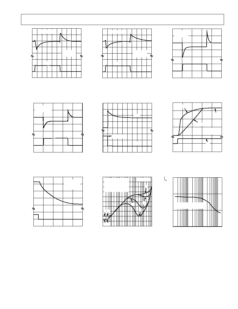
Higher Output Current
The ADP3309 can source up to 100 mA without any heatsink
or pass transistor. If higher current is needed, an appropriate
pass transistor can be used, as in Figure 22, to increase the
output current to 1 A.
ADP3309-3.3
OUT
IN
SD
GND
+
V
IN
= 4V TO 8V
MJE253*
V
OUT
= 3.3V@1A
C1
47 F
C2
10 F
*AAVID531002 HEATSINK IS USED
ERR
R1
50
Figure 22. Higher Output Current Linear Regulator
Constant Dropout Post Regulator
The circuit in Figure 23 provides high precision with low drop-
out for any regulated output voltage. It significantly reduces the
ripple from a switching regulator while providing a constant
dropout voltage, which limits the power dissipation of the LDO
to 30 mW. The ADP3000 used in this circuit is a switching
regulator in the step-up configuration.
+
V
IN
= 2.5V TO 3.5V
C1
100 F
10V
L1
6.8 H
D1
1N5817
C2
100 F
10V
I
LIM
V
IN
SW1
SW2
GND
FB
ADP3000-ADJ
R1
120
R2
30.1k
1%
Q1
2N3906
ADP3309-3.3
IN
OUT
GND
SD
R3
124k
1%
R4
274k
Q2
2N3906
C3
2.2 F
3.3V@100mA
Figure 23. Constant Dropout Post Regulator
ADP3309
8
REV. 0
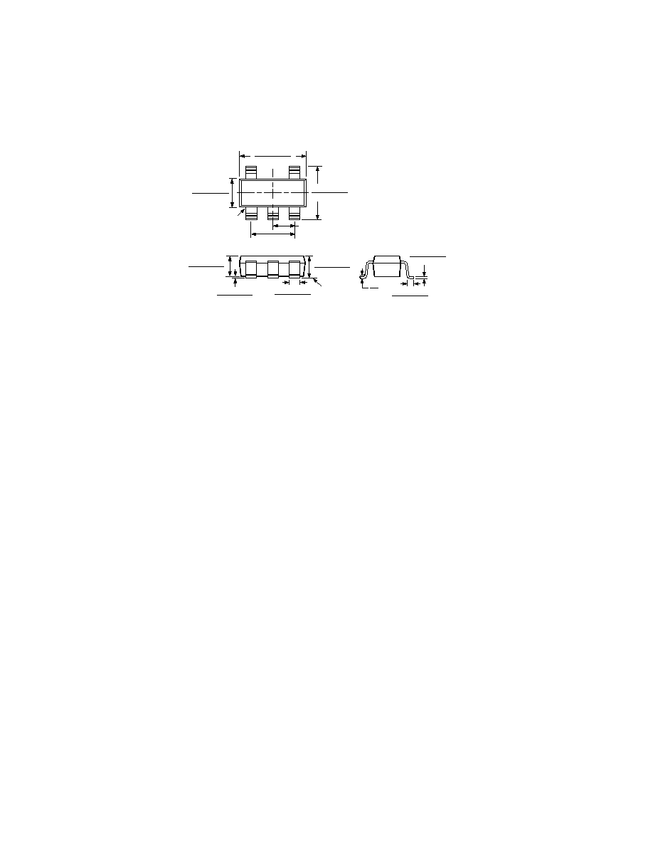
OUTLINE DIMENSIONS
Dimensions shown in inches and (mm).
C32502.57/98
PRINTED IN U.S.A.
5-Lead Surface Mount Package
(SOT-23)
0.1181 (3.00)
0.1102 (2.80)
PIN 1
0.0669 (1.70)
0.0590 (1.50)
0.1181 (3.00)
0.1024 (2.60)
1
3
4
5
0.0748 (1.90)
BSC
0.0374 (0.95) BSC
2
0.0079 (0.20)
0.0031 (0.08)
0.0217 (0.55)
0.0138 (0.35)
10°
0°
0.0197 (0.50)
0.0138 (0.35)
0.0059 (0.15)
0.0019 (0.05)
0.0512 (1.30)
0.0354 (0.90)
SEATING
PLANE
0.0571 (1.45)
0.0374 (0.95)