 | ÐлекÑÑоннÑй компоненÑ: ADP3330 | СкаÑаÑÑ:  PDF PDF  ZIP ZIP |
Äîêóìåíòàöèÿ è îïèñàíèÿ www.docs.chipfind.ru
REV. A
a
ADP3330
One Technology Way, P.O. Box 9106, Norwood, MA 02062-9106, U.S.A.
Tel: 781/329-4700
World Wide Web Site: http://www.analog.com
Fax: 781/326-8703
© Analog Devices, Inc., 1999
Information furnished by Analog Devices is believed to be accurate and
reliable. However, no responsibility is assumed by Analog Devices for its
use, nor for any infringements of patents or other rights of third parties
which may result from its use. No license is granted by implication or
otherwise under any patent or patent rights of Analog Devices.
High Accuracy Ultralow I
Q
,
200 mA, SOT-23, anyCAP
TM
Low Dropout Regulator
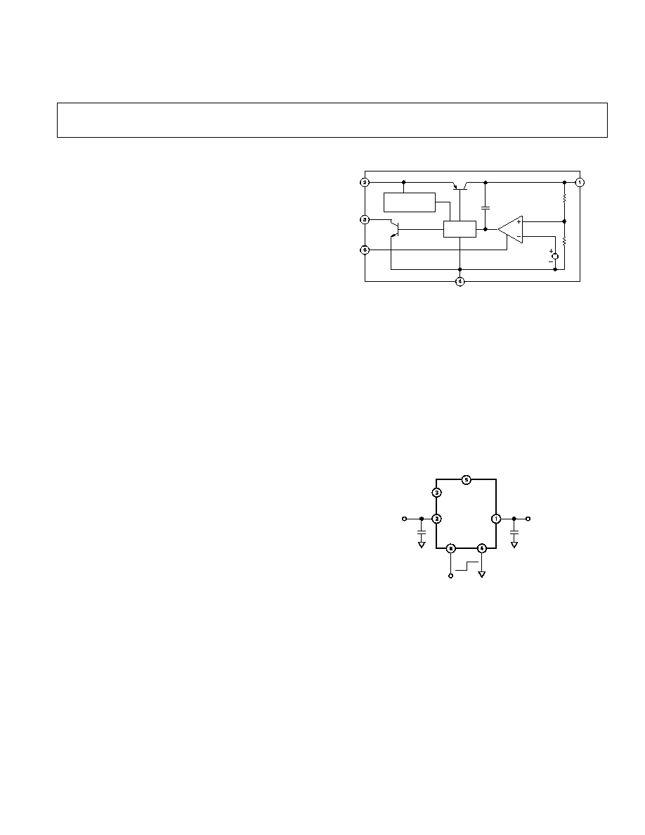
FUNCTIONAL BLOCK DIAGRAM
THERMAL
PROTECTION
CC
IN
ADP3330
OUT
R1
R2
GND
Q1
SD
BANDGAP
REF
DRIVER
g
m
ERR
FEATURES
High Accuracy Over Line and Load: 0.7% @ +25 C,
1.4% Over Temperature
Ultralow Dropout Voltage: 140 mV (Typ) @ 200 mA
Requires Only C
O
= 0.47 F for Stability
anyCAP = Stable with Any Type of Capacitor
(Including MLCC)
Current and Thermal Limiting
Low Noise
Low Shutdown Current: <2 A
2.9 V to 12 V Supply Range
40 C to +85 C Ambient Temperature Range
Ultrasmall Thermally Enhanced Chip-on-LeadTM
SOT-23-6 6-Lead Package
APPLICATIONS
Cellular Telephones
Notebook, Palmtop Computers
Battery Powered Systems
PCMCIA Regulator
Bar Code Scanners
Camcorders, Cameras
GENERAL DESCRIPTION
The ADP3330 is a member of the ADP330x family of precision
low dropout anyCAP voltage regulators. The ADP3330 operates
with an input voltage range of 2.9 V to 12 V and delivers a load
current up to 200 mA. The ADP3330 stands out from the con-
ventional LDOs with a novel architecture and an enhanced
process that enables it to offer performance advantages and
higher output current than its competition. Its patented design
requires only a 0.47
µ
F output capacitor for stability. This
device is insensitive to output capacitor Equivalent Series
Resistance (ESR), and is stable with any good quality capaci-
tor, including ceramic (MLCC) types for space-restricted
applications. The ADP3330 achieves exceptional accuracy of
±
0.7% at room temperature and
±
1.4% over temperature, line
and load variations. The dropout voltage of the ADP3330 is
only 140 mV (typical) at 200 mA. This device also includes a
safety current limit, thermal overload protection and a shutdown
feature. In shutdown mode, the ground current is reduced to
less than 2
µ
A. The ADP3330 has ultralow quiescent current
34
µ
A (typ) in light load situations.
anyCAP and Chip-on-Lead are trademarks of Analog Devices, Inc.
V
OUT
V
IN
+
ADP3330
NR
OUT
ERR
ON
OFF
SD
GND
IN
C
OUT
0.47 F
C
IN
0.47 F
+
Figure 1. Typical Application Circuit
The SOT-23-6 package has been thermally enhanced using
Analog Devices' proprietary Chip-on-Lead feature to maximize
power dissipation.
2
REV. A
ADP3330-xxSPECIFICATIONS
Parameter
Symbol
Conditions
Min
Typ
Max
Units
OUTPUT VOLTAGE ACCURACY
V
OUT
V
IN
= V
OUTNOM
+0.25 V to +12 V
I
L
= 0.1 mA to 200 mA
T
A
= +25
°
C
0.7
+0.7
%
V
IN
= V
OUTNOM
+0.25 V to +12 V
I
L
= 0.1 mA to 150 mA
T
A
= 40
°
C to +85
°
C
1.4
+1.4
%
V
IN
= V
OUTNOM
+0.25 V to +12 V
I
L
= 0.1 mA to 200 mA
T
A
= 20
°
C to +85
°
C
1.4
+1.4
%
LINE REGULATION
V
IN
= V
OUTNOM
+0.25 V to +12 V
T
A
= +25
°
C
0.04
mV/V
LOAD REGULATION
I
L
= 0.1 mA to 200 mA
T
A
= +25
°
C
0.04
mV/mA
GROUND CURRENT
I
GND
I
L
= 200 mA, T
A
= 20
°
C to +85
°
C
1.6
4.0
mA
I
L
= 150 mA
1.2
3.1
mA
I
L
= 50 mA
0.4
1.1
mA
I
L
= 0.1 mA
34
50
µ
A
GROUND CURRENT IN DROPOUT
I
GND
V
IN
= V
OUTNOM
100 mV
I
L
= 0.1 mA
37
55
µ
A
DROPOUT VOLTAGE
V
DROP
V
OUT
= 98% of V
OUTNOM
I
L
= 200 mA, T
A
= 20
°
C to +85
°
C
0.14
0.23
V
I
L
= 150 mA
0.11
0.17
V
I
L
= 10 mA
0.042
0.06
V
I
L
= 1 mA
0.025
0.05
2
V
PEAK LOAD CURRENT
I
LDPK
V
IN
= V
OUTNOM
+ 1 V
300
mA
OUTPUT NOISE
3
V
NOISE
f = 10 Hz100 kHz, C
L
= 10
µ
F
I
L
= 200 mA, C
NR
= 10 nF, V
OUT
= 3 V
47
µ
V rms
f = 10 Hz100 kHz, C
L
= 10
µ
F
I
L
= 200 mA, C
NR
= 0 nF, V
OUT
= 3 V
95
µ
V rms
SHUTDOWN THRESHOLD
V
THSD
ON
2.0
V
OFF
0.4
V
SHUTDOWN PIN INPUT CURRENT
I
SD
V
IN
= 12 V, 0 < SD,
12 V
1.9
9
µ
A
0 < SD,
5 V
1.4
6
µ
A
GROUND CURRENT IN SHUTDOWN
MODE
I
GNDSD
SD = 0 V, V
IN
= 12 V
0.01
2
µ
A
OUTPUT CURRENT IN SHUTDOWN
I
OSD
T
A
= +25
°
C @ V
IN
= 12 V
1
µ
A
MODE
T
A
= +85
°
C @ V
IN
= 12 V
2
µ
A
ERROR PIN OUTPUT LEAKAGE
I
EL
V
EO
= 5 V
1
µ
A
ERROR PIN OUTPUT "LOW"
VOLTAGE
V
EOL
I
SINK
= 400
µ
A
0.19
0.40
V
NOTES
1
Ambient temperature of +85
°
C corresponds to a junction temperature of +125
°
C under typical full load test conditions.
2
Application stable with no load.
3
See detail in Figure 19 and Application section of data sheet.
Specifications subject to change without notice.
(@ T
A
= 40 C to +85 C, V
IN
= +7 V, C
IN
= 0.47 F, C
OUT
= 0.47 F,
unless otherwise noted).
1, 2
The following specifications apply to all voltage options except 2.5.
V
O
V
IN
V
I
O
L
3
REV. A
ADP3330
ADP3330-2.5SPECIFICATIONS
Parameter
Symbol
Conditions
Min
Typ
Max
Units
OUTPUT VOLTAGE ACCURACY
V
OUT
V
IN
= +2.9 V to +12 V
I
L
= 0.1 mA to 200 mA
T
A
= +25
°
C
0.7
+0.7
%
V
IN
= +2.9 V to +12 V
I
L
= 0.1 mA to 150 mA
T
A
= 40
°
C to +85
°
C
1.4
+1.4
%
V
IN
= +2.9 V to +12 V
I
L
= 0.1 mA to 200 mA
T
A
= 20
°
C to +85
°
C
1.4
+1.4
%
LINE REGULATION
V
IN
= +2.9 V to +12 V
T
A
= +25
°
C
0.04
mV/V
LOAD REGULATION
I
L
= 0.1 mA to 200 mA
T
A
= +25
°
C
0.04
mV/mA
GROUND CURRENT
I
GND
I
L
= 200 mA, T
A
= 20
°
C to +85
°
C
1.6
4.0
mA
I
L
= 150 mA
1.2
3.1
mA
I
L
= 50 mA
0.4
1.1
mA
I
L
= 0.1 mA
34
50
µ
A
GROUND CURRENT IN DROPOUT
I
GND
V
IN
= V
OUTNOM
100 mV
I
L
= 0.1 mA
37
55
µ
A
DROPOUT VOLTAGE
V
DROP
V
OUT
= 98% of V
OUTNOM
I
L
= 200 mA, T
A
= 20
°
C to +85
°
C
0.14
0.4
V
I
L
= 150 mA
0.11
0.3
V
I
L
= 10 mA
0.042
0.06
V
I
L
= 1 mA
0.025
0.05
2
V
PEAK LOAD CURRENT
I
LDPK
V
IN
= V
OUTNOM
+ 1 V
300
mA
OUTPUT NOISE
3
V
NOISE
f = 10 Hz100 kHz, C
L
= 10
µ
F
I
L
= 200 mA, C
NR
= 10 nF, V
OUT
= 3 V
47
µ
V rms
f = 10 Hz100 kHz, C
L
= 10
µ
F
I
L
= 200 mA, C
NR
= 0 nF, V
OUT
= 3 V
95
µ
V rms
SHUTDOWN THRESHOLD
V
THSD
ON
2.0
V
OFF
0.4
V
SHUTDOWN PIN INPUT CURRENT
I
SD
V
IN
= 12 V, 0 < SD,
12 V
1.9
9
µ
A
0 < SD,
5 V
1.4
6
µ
A
GROUND CURRENT IN SHUTDOWN
MODE
I
GNDSD
SD = 0 V, V
IN
= 12 V
0.01
2
µ
A
OUTPUT CURRENT IN SHUTDOWN
I
OSD
T
A
= +25
°
C @ V
IN
= 12 V
1
µ
A
MODE
T
A
= +85
°
C @ V
IN
= 12 V
2
µ
A
ERROR PIN OUTPUT LEAKAGE
I
EL
V
EO
= 5 V
1
µ
A
ERROR PIN OUTPUT "LOW"
VOLTAGE
V
EOL
I
SINK
= 400
µ
A
0.19
0.40
V
NOTES
1
Ambient temperature of +85
°
C corresponds to a junction temperature of +125
°
C under typical full load test conditions.
2
Application stable with no load.
3
See detail in Figure 19 and Application section of data sheet.
Specifications subject to change without notice.
(@ T
A
= 40 C to +85 C, V
IN
= +7 V ,C
IN
= 0.47 F, C
OUT
= 0.47 F,
unless otherwise noted).
1, 2
V
O
V
IN
V
I
O
L
ADP3330
4
REV. A
CAUTION
ESD (electrostatic discharge) sensitive device. Electrostatic charges as high as 4000 V readily
accumulate on the human body and test equipment and can discharge without detection.
Although the ADP3330 features proprietary ESD protection circuitry, permanent damage may
occur on devices subjected to high energy electrostatic discharges. Therefore, proper ESD
precautions are recommended to avoid performance degradation or loss of functionality.
ABSOLUTE MAXIMUM RATINGS*
Input Supply Voltage . . . . . . . . . . . . . . . . . . . . 0.3 V to +16 V
Shutdown Input Voltage . . . . . . . . . . . . . . . . . 0.3 V to +16 V
Power Dissipation . . . . . . . . . . . . . . . . . . . . Internally Limited
Operating Ambient Temperature Range . . . . . 40
°
C to +85
°
C
Operating Junction Temperature Range . . . . 40
°
C to +125
°
C
JA
(4-Layer Board) . . . . . . . . . . . . . . . . . . . . . . . +165
°
C/W
JA
(2-Layer Board) . . . . . . . . . . . . . . . . . . . . . . . +190
°
C/W
Storage Temperature Range . . . . . . . . . . . . . 65
°
C to +150
°
C
Lead Temperature Range (Soldering 10 sec) . . . . . . . . +300
°
C
Vapor Phase (60 sec) . . . . . . . . . . . . . . . . . . . . . . . . +215
°
C
Infrared (15 sec) . . . . . . . . . . . . . . . . . . . . . . . . . . . +220
°
C
*This is a stress rating only; operation beyond these limits can cause the device to
be permanently damaged.
ORDERING GUIDE
Voltage
Package
Marking
Model
Output
Option*
Code
ADP3330ART-2.5
2.5 V
RT-6 (SOT-23-6)
L1B
ADP3330ART-2.75 2.75 V
RT-6 (SOT-23-6)
L2B
ADP3330ART-2.85 2.85 V
RT-6 (SOT-23-6)
L3B
ADP3330ART-3
3.0 V
RT-6 (SOT-23-6)
L4B
ADP3330ART-3.3
3.3 V
RT-6 (SOT-23-6)
L5B
ADP3330ART-3.6
3.6 V
RT-6 (SOT-23-6)
L6B
ADP3330ART-5
5.0 V
RT-6 (SOT-23-6)
L8B
*Contact the factory for the availability of other output voltage options.
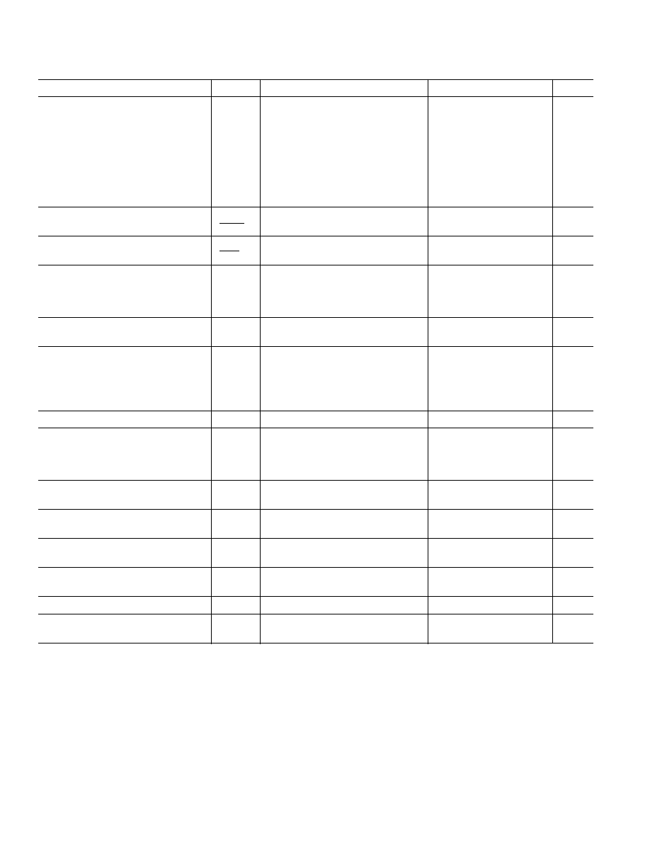
PIN FUNCTION DESCRIPTIONS
Pin
Name
Function
1
OUT
Output of the Regulator. Bypass to ground
with a 0.47
µ
F or larger capacitor.
2
IN
Regulator Input.
3
ERR
Open Collector Output that goes low to
indicate that the output is about to go out
of regulation.
4
GND
Ground Pin.
5
NR
Noise Reduction Pin. Used for further
reduction of output noise (see text for
detail). No connection if not used.
6
SD
Active Low Shutdown Pin. Connect to
ground to disable the regulator output.
When shutdown is not used, this pin
should be connected to the input pin.
PIN CONFIGURATION
TOP VIEW
(Not to Scale)
6
5
4
1
2
3
GND
NR
SD
ERR
IN
OUT
ADP3330
WARNING!
ESD SENSITIVE DEVICE
ADP3330
5
REV. A
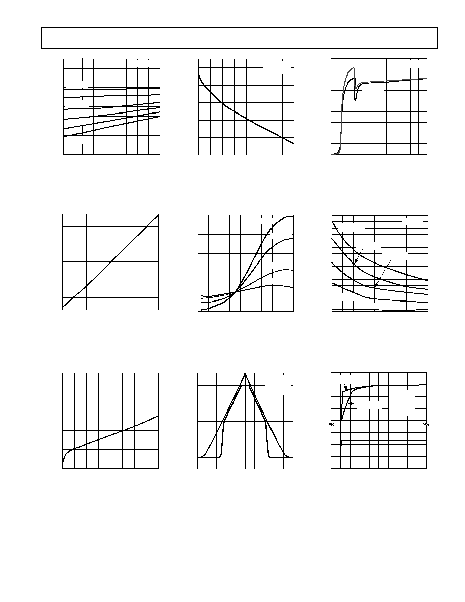
Typical Performance Characteristics
INPUT VOLTAGE Volts
OUTPUT VOLTAGE Volts
3.010
3.002
2.996
3.25 4
5
6
7
8
9
10
11
12
3.008
3.006
3.000
2.998
3.004
2.994
2.992
2.990
V
OUT
= 3.0V
I
L
= 0mA
I
L
= 10mA
I
L
= 100mA
I
L
= 50mA
I
L
= 150mA
I
L
= 200mA
Figure 2. Line Regulation Output
Voltage vs. Supply Voltage
OUTPUT LOAD mA
GROUND CURRENT mA
1.6
1.4
0.6
0
50
200
100
150
1.2
1.0
0.8
V
IN
= 7V
0.4
0.2
0
Figure 5. Ground Current vs. Load
Current
OUTPUT LOAD mA
INPUT/OUTPUT VOLTAGE mV
250
200
0
0
25
100
50
75
150
100
50
125
150
175
200
Figure 8. Dropout Voltage vs.
Output Current
OUTPUT LOAD mA
OUTPUT VOLTAGE Volts
3.005
2.998
0
25
50
75
100
125
150
175 200
3.004
3.003
3.002
3.001
3.000
2.999
V
OUT
= 3.0V
V
IN
= 7V
2.997
2.996
2.995
2.994
Figure 3. Output Voltage vs. Load
Current
0.2
0.4
45 25
135
5
15
35
75
95
115
55
0.1
0.0
0.1
0.3
JUNCTION TEMPERATURE C
OUTPUT VOLTAGE %
I
L
= 50mA
I
L
= 0mA
I
L
= 150mA
I
L
= 200mA
Figure 6. Output Voltage Variation %
vs. Junction Temperature
3.5
3.0
2.5
2.0
1.5
1.0
0.5
0
0
1.0
2.0
3.0
4.0
5.0
INPUT/OUTPUT VOLTAGE Volts
TIME Sec
V
OUT
= 3V
SD
= V
IN
R
L
= 15
Figure 9. Power-Up/Power-Down
INPUT VOLTAGE Volts
GROUND CURRENT
A
45
40
20
0
2
4
6
8
10
12
35
30
25
V
OUT
= 3V
15
10
5
0
I
L
= 100 A
I
L
= 0 A
Figure 4. Ground Current vs. Supply
Voltage
JUNCTION TEMPERATURE C
GROUND CURRENT mA
3.0
2.8
0
45 25
115
5
15
35
55
75
95
2.6
2.4
2.2
2.0
1.8
1.6
1.4
1.2
1.0
0.8
0.6
0.4
0.2
135
V
IN
= 7V
I
L
= 0mA
I
L
= 100mA
I
L
= 50mA
I
L
= 150mA
I
L
= 200mA
Figure 7. Ground Current vs. Junction
Temperature
3
2
1
0
10
5
0
0
100
200
300
400
500
V
OUT
Volts
V
IN
Volts
TIME s
V
IN
= 7V
V
OUT
= 3V
SD
= V
IN
R
L
= 15
C
L
= 10 F
C
L
= 0.47 F
Figure 10. Power-Up Response