 | ÐлекÑÑоннÑй компоненÑ: ADP3331 | СкаÑаÑÑ:  PDF PDF  ZIP ZIP |
Äîêóìåíòàöèÿ è îïèñàíèÿ www.docs.chipfind.ru
REV. 0
Information furnished by Analog Devices is believed to be accurate and
reliable. However, no responsibility is assumed by Analog Devices for its
use, nor for any infringements of patents or other rights of third parties
which may result from its use. No license is granted by implication or
otherwise under any patent or patent rights of Analog Devices.
a
ADP3331
One Technology Way, P.O. Box 9106, Norwood, MA 02062-9106, U.S.A.
Tel: 781/329-4700
World Wide Web Site: http://www.analog.com
Fax: 781/326-8703
© Analog Devices, Inc., 1999
Adjustable Output Ultralow I
Q
, 200 mA,
SOT-23, anyCAPTM Low Dropout Regulator
FUNCTIONAL BLOCK DIAGRAM
THERMAL
PROTECTION
CC
IN
ADP3331
OUT
GND
Q1
SD
BANDGAP
REF
DRIVER
g
m
ERR
FB
Q2
FEATURES
High Accuracy Over Line and Load: 0.7% @ +25 C,
1.4% Over Temperature
Ultralow Dropout Voltage: 140 mV (Typ) @ 200 mA
Can Be Used as a High Current (>1 A) LDO
Controller
Requires Only C
O
= 0.47 F for Stability
anyCAP = Stable with Any Type of Capacitor
(Including MLCC)
Current and Thermal Limiting
Low Noise
Low Shutdown Current: <2 A
2.6 V to 12 V Supply Range
1.5 V to 10 V Output Range
40 C to +85 C Ambient Temperature Range
Ultrasmall Thermally Enhanced Chip-on-LeadTM
SOT-23-6 Lead Package
APPLICATIONS
Cellular Telephones
Notebook, Palmtop Computers
Battery Powered Systems
PCMCIA Regulator
Bar Code Scanners
Camcorders, Cameras
GENERAL DESCRIPTION
The ADP3331 is a member of the ADP330x family of preci-
sion low dropout anyCAP voltage regulators. The ADP3331
operates with an input voltage range of 2.6 V to 12 V and deliv-
ers a load current up to 200 mA. The ADP3331 stands out
from the conventional LDOs with a novel architecture and an
enhanced process that enables it to offer performance advan-
tages and higher output current than its competition. Its pat-
ented design requires only a 0.47
µ
F output capacitor for
stability. This device is insensitive to capacitor Equivalent
Series Resistance (ESR), and is stable with any good quality
capacitor, including ceramic (MLCC) types for space restricted
applications. The ADP3331 achieves exceptional accuracy of
±
0.7% at room temperature and
±
1.4% overall accuracy over
temperature, line and load variations. The dropout voltage of
the ADP3331 is only 140 mV (typical) at 200 mA. This device
also includes a safety current limit, thermal overload protection
and a shutdown feature. In shutdown mode, the ground current is
reduced to less than 2
µ
A. The ADP3331 has ultralow quies-
cent current 34
µ
A (typical) in light load situations. The
SOT-23-6 package has been thermally enhanced using Analog
Device's proprietary Chip-on-Lead feature to maximize power
dissipation.
anyCAP and Chip-on-Lead are trademarks of Analog Devices, Inc.
V
OUT
V
IN
+
ADP3331
FB
OUT
ERR
ON
OFF
SD
GND
IN
C 2
0.47 F
C 1
0.47 F
+
E
OUT
R 3
330k
R1
R2
Figure 1. Typical Application Circuit
REV. 0
2
ADP3331SPECIFICATIONS
Parameter
Symbol
Conditions
Min
Typ
Max
Units
OUTPUT VOLTAGE ACCURACY
3
V
IN
= V
OUTNOM
+ 0.25 V to 12 V,
HIGH OUTPUT VOLTAGE RANGE
V
OUTNOM
2.35 V,
I
L
= 0.1 mA to 200 mA,
T
A
= +25
°
C
0.7
+0.7
%
V
IN
= V
OUTNOM
+ 0.25 V to 12 V,
V
OUTNOM
2.35 V,
I
L
= 0.1 mA to 150 mA,
T
A
= 40
°
C to +85
°
C
1.4
+1.4
%
V
IN
= V
OUTNOM
+ 0.25 V to 12 V,
V
OUTNOM
2.35 V,
I
L
= 0.1 mA to 200 mA,
T
A
= 20
°
C to +85
°
C
1.4
+1.4
%
OUTPUT VOLTAGE ACCURACY
3
V
IN
= 2.6 V to 12 V,
LOW OUTPUT VOLTAGE RANGE
V
OUTNOM
= 1.5 V to 2.35 V,
I
L
= 0.1 mA to 200 mA,
T
A
= +25
°
C
0.7
+0.7
%
V
IN
= 2.6 V to 12 V,
V
OUTNOM
= 1.5 V to 2.35 V,
I
L
= 0.1 mA to 150 mA,
T
A
= 40
°
C to +85
°
C
1.4
+1.4
%
V
IN
= 2.6 V to 12 V,
V
OUTNOM
= 1.5 V to 2.35 V,
I
L
= 0.1 mA to 200 mA,
T
A
= 20
°
C to +85
°
C
1.4
+1.4
%
LINE REGULATION
V
O
V
IN
= V
OUTNOM
+0.25 V to 12 V
V
IN
T
A
= +25
°
C
0.06
mV/V
LOAD REGULATION
V
O
I
L
= 0.1 mA to 200 mA
I
L
T
A
= +25
°
C
0.04
mV/mA
GROUND CURRENT
I
GND
I
L
= 200 mA, T
A
= 20
°
C to +85
°
C
1.6
4.0
mA
I
L
= 150 mA
1.2
3.1
mA
I
L
= 50 mA
0.4
1.1
mA
I
L
= 0.1 mA
34
50
µ
A
GROUND CURRENT
I
GND
V
IN
= V
OUTNOM
100 mV
IN DROPOUT
I
L
= 0.1 mA
37
55
µ
A
DROPOUT VOLTAGE
V
DROP
V
OUT
= 98% of V
OUTNOM
I
L
= 200 mA, T
A
= 20
°
C to +85
°
C
0.14
0.23
V
I
L
= 150 mA
0.11
0.17
V
I
L
= 10 mA
0.042 0.06
V
I
L
= 1 mA
0.025 0.05
2
V
PEAK LOAD CURRENT
I
LDPK
V
IN
= V
OUTNOM
+ 1 V
300
mA
OUTPUT NOISE
V
NOISE
f = 10 Hz100 kHz, C
L
= 10
µ
F
I
L
= 200 mA, C
NR
= 10 nF, V
OUT
= 3 V
47
µ
V rms
f = 10 Hz100 kHz, C
L
= 10
µ
F
I
L
= 200 mA, C
NR
= 0 nF, V
OUT
= 3 V
95
µ
V rms
SHUTDOWN THRESHOLD
V
TH
SD
ON
2.0
V
OFF
0.4
V
SHUTDOWN PIN INPUT CURRENT
I
SD
0 <
SD
12 V
1.9
9
µ
A
0 <
SD
5 V
1.4
6
µ
A
GROUND CURRENT IN
SHUTDOWN MODE
I
GND
SD
SD = 0 V, V
IN
= 12 V
0.01
2
µ
A
(@T
A
= 40 C to +85 C, V
IN
= 7 V, C
IN
= 0.47 F, C
OUT
= 0.47 F, unless otherwise
noted)
1, 2
REV. 0
3
ADP3331
Parameter
Symbol
Conditions
Min
Typ
Max
Units
OUTPUT CURRENT IN
I
O
SD
T
A
= +25
°
C @ V
IN
= 12 V
1
µ
A
SHUTDOWN MODE
T
A
= +85
°
C @ V
IN
= 12 V
2
µ
A
ERROR PIN OUTPUT LEAKAGE
I
EL
V
EO
= 5 V
1
µ
A
ERROR PIN OUTPUT
"LOW" VOLTAGE
V
EOL
I
SINK
= 400
µ
A
0.19
0.40
V
NOTES
1
Ambient temperature of +85
°
C corresponds to a junction temperature of +125
°
C under typical full load test conditions.
2
Application stable with no load.
3
Assumes the use of ideal resistors. Overall accuracy also depends on the tolerance of the external resistors used to set the output voltage.
Specifications subject to change without notice.
ABSOLUTE MAXIMUM RATINGS*
Input Supply Voltage . . . . . . . . . . . . . . . . . . . . . 0.3 to +16 V
Shutdown Input Voltage . . . . . . . . . . . . . . . . . . 0.3 to +16 V
Power Dissipation . . . . . . . . . . . . . . . . . . . . Internally Limited
Operating Ambient Temperature Range . . . . 40
°
C to +85
°
C
Operating Junction Temperature Range . . . 40
°
C to +125
°
C
JA
(4-Layer Board) . . . . . . . . . . . . . . . . . . . . . . . 165
°
C/W
JA
(2-Layer Board) . . . . . . . . . . . . . . . . . . . . . . . 190
°
C/W
Storage Temperature Range . . . . . . . . . . . . 65
°
C to +150
°
C
Lead Temperature Range (Soldering 10 sec) . . . . . . . . +300
°
C
Vapor Phase (60 sec) . . . . . . . . . . . . . . . . . . . . . . . . +215
°
C
Infrared (15 sec) . . . . . . . . . . . . . . . . . . . . . . . . . . . .+220
°
C
*This is a stress rating only; operation beyond these limits can cause the device to
be permanently damaged.
ORDERING GUIDE
Output
Marking
Model
Voltage
Package Option
Code
ADP3331ART
ADJ
RT-6 (SOT-23-6)
L9B
CAUTION
ESD (electrostatic discharge) sensitive device. Electrostatic charges as high as 4000 V readily
accumulate on the human body and test equipment and can discharge without detection.
Although the ADP3331 features proprietary ESD protection circuitry, permanent damage may
occur on devices subjected to high energy electrostatic discharges. Therefore, proper ESD
precautions are recommended to avoid performance degradation or loss of functionality.
WARNING!
ESD SENSITIVE DEVICE
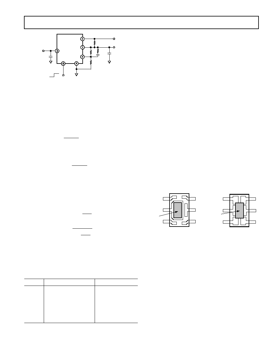
PIN FUNCTION DESCRIPTIONS
Pin
Name
Function
1
OUT
Output of the Regulator. Bypass to ground
with a 0.47
µ
F or larger capacitor.
2
IN
Regulator Input.
3
ERR
Open Collector Output that goes low to
indicate that the output is about to go out
of regulation.
4
GND
Ground.
5
FB
Feedback Input. Connect to an external
resistor divider which sets the output
voltage.
6
SD
Active Low Shutdown Pin. Connect to
ground to disable the regulator output.
When shutdown is not used, this pin
should be connected to the input pin.
PIN CONFIGURATION
TOP VIEW
(Not to Scale)
6
5
4
1
2
3
GND
FB
SD
ERR
IN
OUT
ADP3331
REV. 0
ADP3331
4
Typical Performance Characteristics
INPUT VOLTAGE Volts
OUTPUT VOLTAGE Volts
3.010
3.002
2.996
3.25 4
5
6
7
8
9
10
11
12
3.008
3.006
3.000
2.998
3.004
2.994
2.992
2.990
V
OUT
= 3.0V
I
L
= 0mA
I
L
= 10mA
I
L
= 100mA
I
L
= 50mA
I
L
= 150mA
I
L
= 200mA
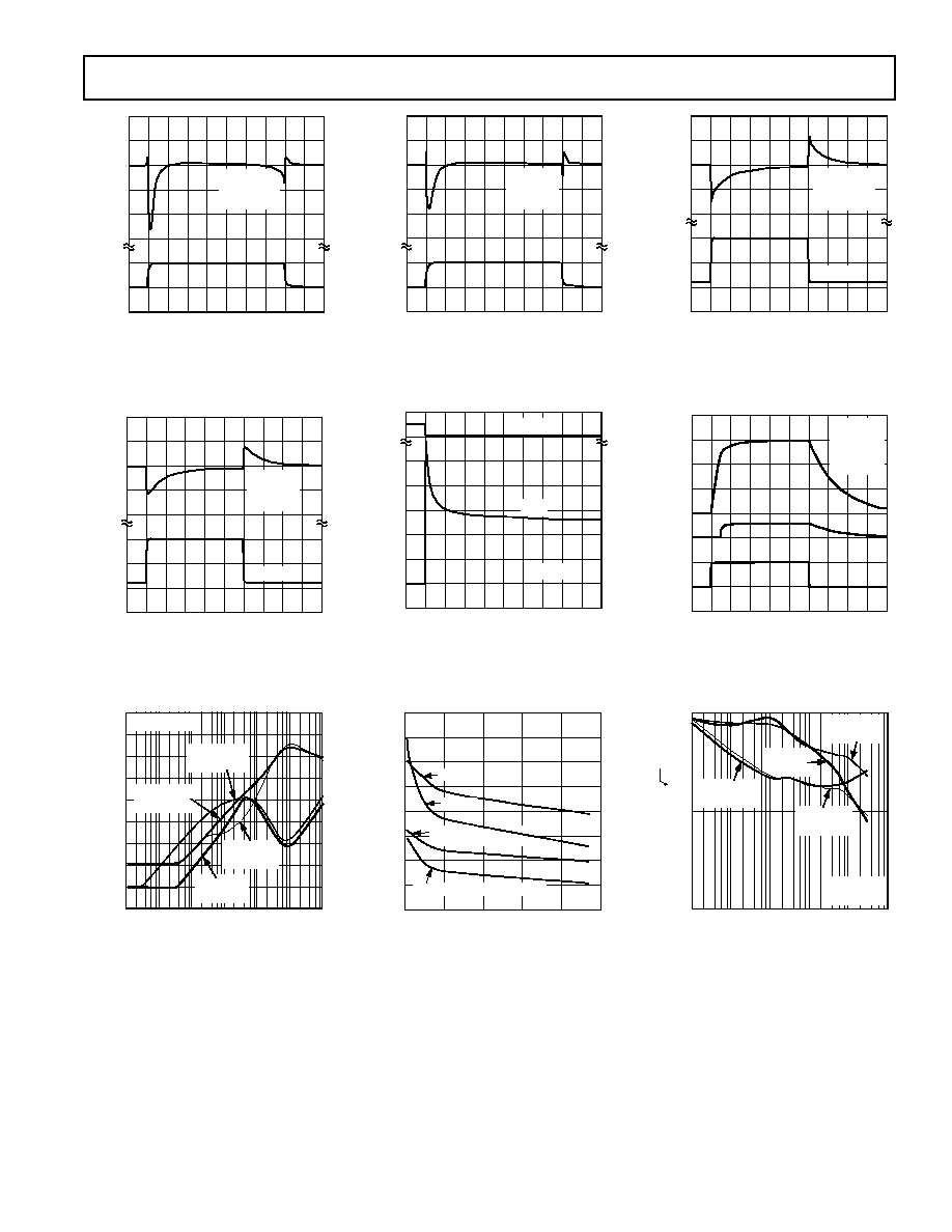
Figure 2. Line Regulation Output
Voltage vs. Supply Voltage
OUTPUT LOAD mA
GROUND CURRENT mA
1.6
1.4
0.6
0
50
200
100
150
1.2
1.0
0.8
V
IN
= 7V
0.4
0.2
0
Figure 5. Ground Current vs. Load
Current
OUTPUT LOAD mA
INPUT/OUTPUT VOLTAGE mV
250
200
0
0
25
100
50
75
150
100
50
125
150
175
200
Figure 8. Dropout Voltage vs.
Output Current
OUTPUT LOAD mA
OUTPUT VOLTAGE Volts
3.005
2.998
0
25
50
75
100
125
150
175 200
3.004
3.003
3.002
3.001
3.000
2.999
V
OUT
= 3.0V
V
IN
= 7V
2.997
2.996
2.995
2.994
Figure 3. Output Voltage vs. Load
Current
0.2
0.4
45 25
135
5
15
35
75
95
115
55
0.1
0.0
0.1
0.3
JUNCTION TEMPERATURE C
OUTPUT VOLTAGE %
I
L
= 50mA
I
L
= 0mA
I
L
= 150mA
I
L
= 200mA
Figure 6. Output Voltage Variation %
vs. Junction Temperature
3.5
3.0
2.5
2.0
1.5
1.0
0.5
0
0
1.0
2.0
3.0
4.0
5.0
INPUT/OUTPUT VOLTAGE Volts
TIME Sec
V
OUT
= 3V
SD
= V
IN
R
L
= 15
Figure 9. Power-Up/Power-Down
INPUT VOLTAGE Volts
GROUND CURRENT
A
45
40
20
0
2
4
6
8
10
12
35
30
25
V
OUT
= 3V
15
10
5
0
I
L
= 100 A
I
L
= 0 A
Figure 4. Ground Current vs. Supply
Voltage
JUNCTION TEMPERATURE C
GROUND CURRENT mA
3.0
2.8
0
45 25
115
5
15
35
55
75
95
2.6
2.4
2.2
2.0
1.8
1.6
1.4
1.2
1.0
0.8
0.6
0.4
0.2
135
V
IN
= 7V
I
L
= 0mA
I
L
= 100mA
I
L
= 50mA
I
L
= 150mA
I
L
= 200mA
Figure 7. Ground Current vs. Junction
Temperature
3
2
1
0
10
5
0
0
100
200
300
400
500
V
OUT
Volts
V
IN
Volts
TIME s
V
IN
= 7V
V
OUT
= 3V
SD
= V
IN
R
L
= 15
C
L
= 10 F
C
L
= 0.47 F
Figure 10. Power-Up Response
REV. 0
ADP3331
5
3.040
3.000
2.960
2.920
7.5
7.0
0
100
200
300
400
500
TIME s
V
OUT
Volts
V
IN
Volts
V
OUT
= 3V
R
L
= 15
C
L
= 0.47 F
Figure 11. Line Transient Response
3.100
3.050
3.000
2.950
2.900
200
100
0
0
200
400
600
800
1000
Volts
mA
TIME s
V
IN
= 7V
V
OUT
= 3V
C
L
= 10 F
20mA
Figure 14. Load Transient Response
FREQUENCY Hz
RIPPLE REJECTION dB
0
10
100
1k
10k
100k
1M
10M
10
20
30
40
50
60
70
80
90
C
L
= 0.47 F
I
L
= 0.1mA
C
L
= 0.47 F
I
L
= 200mA
C
L
= 10 F
I
L
= 200mA
C
L
= 10 F
I
L
= 0.1mA
V
OUT
= 3.0V
Figure 17. Power Supply Ripple
Rejection
3.040
3.000
2.960
2.920
7.5
7.0
0
100
200
300
400
500
TIME s
V
OUT
Volts
V
IN
Volts
V
OUT
= 3V
R
L
= 15
C
L
= 10 F
Figure 12. Line Transient Response
3
0
500
400
300
200
100
0
Volts
mA
0
0.5 1.0 1.5 2.0 2.5 3.0 3.5 4.0 4.5 5.0
TIME Sec
V
OUT
I
OUT
V
IN
= 7V
Figure 15. Short Circuit Current
120
160
0
50
10
20
30
40
100
80
60
140
C
L
F
RMS NOISE
V
40
20
0
I
L
= 0mA WITH NOISE REDUCTION
I
L
= 200mA
I
L
= 200mA
WITH NOISE REDUCTION
I
L
= 0mA
Figure 18. RMS Noise vs. C
L
(10 Hz100 kHz)
3.100
3.050
3.000
2.950
2.900
200
100
0
0
200
400
600
800
1000
Volts
mA
TIME s
V
IN
= 7V
V
OUT
= 3V
C
L
= 0.47 F
20mA
Figure 13. Load Transient Response
3
2
1
0
0
2
0
3
Volts
V
OUT
V
ERR
V
SD
0
200
400
600
800
1000
TIME s
V
IN
= 7V
V
OUT
= 3V
C
L
= 10 F
R
L
= 15
Figure 16. Turn OnTurn Off Response
FREQUENCY Hz
VOLTAGE NOISE SPECTRAL
DENSITY
V/ Hz
1
0.01
10
100
1M
0.1
1k
10k
100k
V
OUT
= 3.0V
I
L
= 200mA
C
L
= 0.47 F
C
NR
= 0
C
L
= 10 F
C
NR
= 0
C
L
= 0.47 F
C
NR
= 10nF
C
L
= 10 F
C
NR
= 10nF
Figure 19. Output Noise Density
REV. 0
ADP3331
6
THEORY OF OPERATION
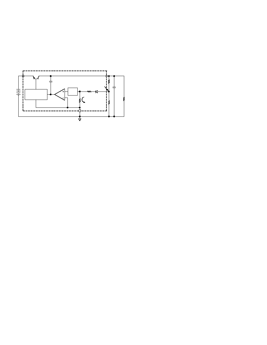
The new ADP3331 anyCAP LDO uses a single control loop for
both regulation and reference functions as shown in Figure 20.
The output voltage is sensed by an external resistive voltage
divider consisting of R1 and R2. Feedback is taken from this
network by way of a series diode (D1) and a second resistor
divider (R3 and R4) to the input of an amplifier.
PTAT
V
OS
g
m
NONINVERTING
WIDEBAND
DRIVER
INPUT
Q1
ADP3331
COMPENSATION
CAPACITOR
ATTENUATION
(V
BANDGAP
/V
OUT
)
R1
D1
R2
R3
R4
OUTPUT
PTAT
CURRENT
R
LOAD
C
LOAD
(a)
GND
Figure 20. Functional Block Diagram
A very high gain error amplifier is used to control this loop. The
amplifier is constructed in such a way that at equilibrium it
produces a large, temperature-proportional input "offset voltage"
that is repeatable and very well controlled. The temperature-
proportional offset voltage is combined with the complementary
diode voltage to form a "virtual bandgap" voltage, implicit in
the network, although it never appears explicitly in the circuit.
Ultimately, this patented design makes it possible to control the
loop with only one amplifier. This technique also improves the
noise characteristics of the amplifier by providing more flexibil-
ity on the trade-off of noise sources that leads to a low noise
design.
The R1, R2 divider is chosen in the same ratio as the bandgap
voltage to output voltage. Although the R1, R2 resistor divider
is loaded by the diode D1 and a second divider consisting of R3
and R4, the values are chosen to produce a temperature stable
output. This unique arrangement specifically corrects for the
loading of the divider so that the error resulting from the base
current loading in conventional circuits is avoided.
The patented amplifier controls a new and unique noninverting
driver that drives the pass transistor, Q1. The use of this special
noninverting driver enables the frequency compensation to
include the load capacitor in a pole-splitting arrangement to
achieve reduced sensitivity to the value, type and ESR of the
load capacitor.
Most LDOs place strict requirements on the range of ESR
values for the output capacitor because they are difficult to
stabilize due to the uncertainty of the load capacitance and
resistance. Moreover, the ESR value required to keep conven-
tional LDOs stable, changes depending on load and tempera-
ture. These ESR limitations make designing with LDOs more
difficult because of their unclear specifications and extreme
variations over temperature.
This is no longer true with the ADP3331. It can be used with
any good quality capacitor, with no constraint on the minimum
ESR. The innovative design allows the circuit to be stable with
just a small 0.47
µ
F capacitor on the output. Additional advan-
tages of the pole-splitting scheme include superior line noise
rejection and very high regulator gain. The high gain leads to
excellent regulation, and
±
1.4% accuracy is guaranteed over
line, load and temperature.
Additional features of the circuit include current limit, thermal
shutdown and an error flag. Compared to standard solutions
that give a warning after the output has lost regulation, the
ADP3331 provides improved system performance by enabling
the
ERR pin to give a warning just before the device loses
regulation.
As the chip's temperature rises above +165
°
C, the circuit acti-
vates a soft thermal shutdown to reduce the current to a safe
level. The thermal shutdown condition is indicated by the
ERR
signal going low.
APPLICATION INFORMATION
Capacitor Selection
Output Capacitor: The stability and transient response of the
LDO is a function of the output capacitor. The ADP3331 is
stable with a wide range of capacitor values, types and ESR
(anyCAP). A capacitor as low as 0.47
µ
F is all that is needed for
stability; larger capacitors can be used if high current surges on
the output are anticipated. The ADP3331 is stable with ex-
tremely low ESR capacitors (ESR
0), such as Multilayer
Ceramic Capacitors (MLCC) or OSCON. Note that the effec-
tive capacitance of some capacitor types fall below the minimum
over temperature or with DC voltage.
Input Capacitor: An input bypass capacitor is not strictly re-
quired but it is recommended in any application involving long
input wires or high source impedance. Connecting a 0.47
µ
F
capacitor from the input to ground reduces the circuit's sensitiv-
ity to PC board layout and input transients. If a larger output
capacitor is necessary, a larger value input capacitor is also
recommended.
Noise Reduction Capacitor: A noise reduction capacitor can be
used to reduce the output noise by 6 dB to 10 dB. This capaci-
tor limits the noise gain when connected between the feedback
pin (FB) and the output pin (OUT) as shown in Figure 21. Low
leakage capacitors in the 10 pF to 500 pF range provide the best
performance. Since FB is internally connected to a high imped-
ance node, any connection to this node should be carefully done
to avoid noise pickup from external sources. The pad connected
to this pin should be as small as possible and long PC board
traces are not recommended. When adding a noise reduction
capacitor, use the following guidelines:
·
Maintain a minimum load current of 1 mA when not in
shutdown
·
For CNR values greater than 500 pF, add a 100 k
series
resistor (RNR).
It is important to note that as CNR increases, the turn-on time
will be delayed. With CNR values greater than 1 nF, this delay
may be on the order of several milliseconds.
REV. 0
ADP3331
7
V
OUT
V
IN
+
ADP3331
FB
OUT
ERR
ON
OFF
SD
GND
IN
C 2
0.47 F
C 1
0.47 F
+
E
OUT
R3
R1
R2
R
N R
C
N R
Figure 21. Noise Reduction Circuit
Output Voltage
The ADP3331 has an adjustable output voltage that can be set
by an external resistor divider. The output voltage will be di-
vided by R1 and R2, and then fed back to the FB pin. Refer to
Figure 21.
In order to have the lowest possible sensitivity of the output
voltage to temperature variations, it is important that the paral-
lel resistance of R1 and R2 is always 230 k
:
R
R
R
R
k
1
2
1
2
230
×
+
=
Also, for the best accuracy over temperature the feedback volt-
age should set for 1.204 V:
V
R
R
R
V
OUT
FB
2
1
2
+
=
where V
OUT
is the desired output voltage and V
FB
is the "virtual
bandgap" voltage. Note that V
FB
does not actually appear at the
FB pin due to loading by the internal PTAT current.
Combining the above equations and solving for R1 and R2 gives
the following formulas:
R
V
V
k
R
V
V
k
OUT
FB
FB
OUT
1
230
2
230
1
=
=
-
The output voltage can be adjusted to any voltage from 1.5 V to
10 V. For example, the Feedback Resistor Selection Table shows
some representative feedback resistor values for output voltages
in the specified range.
Table I. Feedback Resistor Selection
V
OUT
R1 (1% Resistor)
R2 (1% Resistor)
1.5 V
243 k
1.00 M
1.8 V
340 k
698 k
2.2 V
422 k
511 k
2.7 V
511 k
412 k
3.3 V
634 k
365 k
5 V
953 k
301 k
9 V
1.00 M
154 k
Output voltages above 5 V and below 1.6 V will require non-
standard resistor values or adding an additional resistor to the
divider network to achieve the best performance. Using stan-
dard values as shown in Table I will sacrifice some temperature
stability.
Output Current Limit
The ADP3331 is short circuit protected by limiting the pass
transistor's base drive current. The maximum output current is
limited to about 300 mA.
Thermal Overload Protection
The ADP3331 is protected against damage due to excessive
power dissipation by its thermal overload protection circuit.
Thermal protection limits the die temperature to a maximum of
+165
°
C. Under extreme conditions (i.e., high ambient tempera-
ture and power dissipation) where the die temperature starts to
rise above +165
°
C, the output current will be reduced until the
die temperature has dropped to a safe level.
Current and thermal limit protections are intended to protect
the device against accidental overload conditions. For normal
operation, the device's power dissipation should be externally
limited so that the junction temperature will not exceed 125
°
C.
Chip-on-Lead
The ADP3331 uses a patented Chip-on-Lead package design to
ensure the best thermal performance in an SOT-23 footprint.
The standard SOT-23 depends on the majority of the heat to
flow out of the ground pin. The Chip-on-Lead package uses an
electrically isolated die attach, which allows all the pins to
contribute to heat conduction. This technique reduces the ther-
mal resistance to 190
°
C/W on a 2-layer board as compared to
>230
°
C/W for a standard SOT-23 lead frame. Figure 22 shows
the difference between the standard SOT-23 and the Chip-on-
Lead lead frames.
SILICON DIE
WITH
ELECTRICALLY
ISOLATED
DIE ATTACH
SILICON
DIE
NORMAL SOT-23-6 PACKAGE
THERMALLY ENHANCED
CHIP-ON-LEAD PACKAGE
Figure 22. Chip-on-Lead Package
Calculating Junction Temperature
Device power dissipation is calculated as follows:
P
D
= (V
IN
V
OUT
) I
LOAD
+ (V
IN
) I
GND
Where I
LOAD
and I
GND
are load current and ground current, V
IN
and V
OUT
are the input and output voltages respectively.
Assuming the worst case operating conditions are I
LOAD
=
200 mA, I
GND
= 4 mA, V
IN
= 4.2 V and V
OUT
= 3.0 V, the
device power dissipation is:
P
D
= (4.2 V 3.0 V) 200 mA + (4.2 V) 4 mA = 257 mW
The proprietary package used on the ADP3331 has a thermal
resistance of 165
°
C/W when placed on a 4-layer board, and
190
°
C/W when placed on a 2-layer board. This allows the ambi-
ent temperature to be significantly higher for a given power
dissipation than with a standard package. Assuming a 4-layer
board, the junction temperature rise above ambient will be
approximately equal to:
T
JA
= 0.257 W
×
165
°
C/W = 42.4
°
C
REV. 0
ADP3331
8
To limit the junction temperature to 125
°
C, the maximum
allowable ambient temperature is:
T
A(MAX)
= +125
°
C 42.4
°
C = +82.6
°
C
Shutdown Mode
Applying a TTL level high signal to the shutdown (
SD) pin, or
tying it to the input pin, will turn the output ON. Pulling the
SD to 0.4 V or below, or tying it to ground, will turn the output
OFF. In shutdown mode, the quiescent current is reduced to
less than 1
µ
A.
Error Flag Dropout Detector
The ADP3331 will maintain its output voltage over a wide
range of load, input voltage, and temperature conditions. If the
output is about to lose regulation, due to the input voltage ap-
proaching the dropout level, the error flag will be activated. The
ERR output is an open collector, which will be driven low.
Once set, the
ERR flag's hysteresis will keep the output low
until a small margin of operating range is restored either by
raising the supply voltage or reducing the load.
Low Voltage Applications
In applications where the output voltage is 2.2 V or less, the
ADP3331 may begin to exhibit some turn-on overshoot. The
degree of overshoot is determined by several factors: the output
voltage setting, the output load, the noise reduction capacitor,
and the output capacitor.
The output voltage setting is determined by the application and
cannot be tailored for minimum overshoot. In general, for out-
put voltages 2.2 V or less, the overshoot becomes larger as the
output voltage decreases.
The output load is also determined by the system requirements.
However, if the ADP3331 has no load on the output during
start-up, a small amount of preload can be added to minimize
overshoot. A preload of 2
µ
A to 20
µ
A is recommended.
A noise reduction capacitor, if not already being used, is sug-
gested to reduce the overshoot. Values in the range of 10 pF to
100 pF works best along with the preload suggested previously.
The output capacitor can be adjusted to minimize the over-
shoot. Values in the 0.47
µ
F to 1.0
µ
F range should be used in
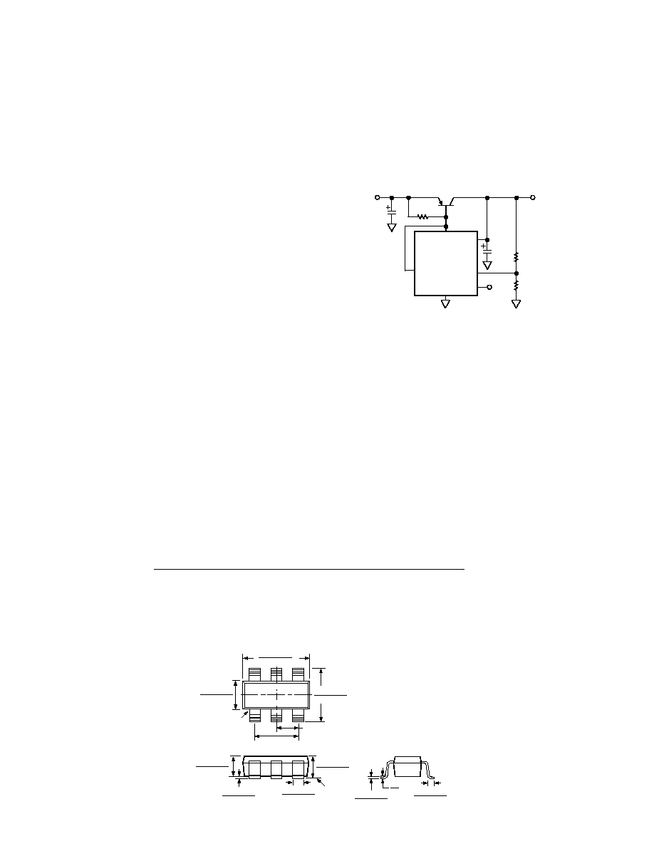
OUTLINE DIMENSIONS
Dimensions shown in inches and (mm).
6-Lead Surface Mount
RT-6 (SOT-23-6)
0.122 (3.10)
0.106 (2.70)
PIN 1
0.071 (1.80)
0.059 (1.50)
0.118 (3.00)
0.098 (2.50)
0.075 (1.90)
BSC
0.037 (0.95) BSC
1
3
4
5
6
2
0.009 (0.23)
0.003 (0.08)
0.022 (0.55)
0.014 (0.35)
10°
0°
0.020 (0.50)
0.010 (0.25)
0.059 (0.15)
0.000 (0.00)
0.051 (1.30)
0.035 (0.90)
SEATING
PLANE
0.057 (1.45)
0.035 (0.90)
C36242.56/99
PRINTED IN U.S.A.
conjunction with the preload and noise reduction capacitor.
Further increases in the output capacitance may be acceptable if
the output already has a sizable load during start-up.
Higher Output Current
The ADP3331 can source up to 200 mA without any heat sink
or pass transistor. If higher current is needed, an appropriate
pass transistor can be used, as in Figure 23, to increase the
output current to 1 A.
V
IN
= 3.3V
V
OUT
= 1.8V @ 1A
MJE253*
C2
10 F
C1
47 F
R1
50
*REQUIRES HEAT SINK
IN
OUT
ERR
GND
SD
ADP3331
FB
340k
698k
Figure 23. High Output Current Linear Regulator
Printed Circuit Board Layout Considerations
Use the following general guidelines when designing printed
circuit boards:
1. PC board traces with larger cross sectional areas will remove
more heat from the ADP3331. For optimum heat transfer,
specify thick copper and use wide traces.
2. The thermal resistance can be decreased by approximately
10% by adding a few square centimeters of copper area to
the lands connected to the pins of the LDO.
3. The feedback pin is a high impedance input, and care should
be taken when making a connection to this pin. The voltage
setting resistors and noise reduction network must be located
as close as possible. Long PC board traces are not recom-
mended. Avoid routing traces near possible noise sources.