 | ÐлекÑÑоннÑй компоненÑ: ADP3339 | СкаÑаÑÑ:  PDF PDF  ZIP ZIP |
Äîêóìåíòàöèÿ è îïèñàíèÿ www.docs.chipfind.ru
REV. 0
Information furnished by Analog Devices is believed to be accurate and
reliable. However, no responsibility is assumed by Analog Devices for its
use, nor for any infringements of patents or other rights of third parties that
may result from its use. No license is granted by implication or otherwise
under any patent or patent rights of Analog Devices.
a
ADP3339
One Technology Way, P.O. Box 9106, Norwood, MA 02062-9106, U.S.A.
Tel: 781/329-4700
www.analog.com
Fax: 781/326-8703
© Analog Devices, Inc., 2001
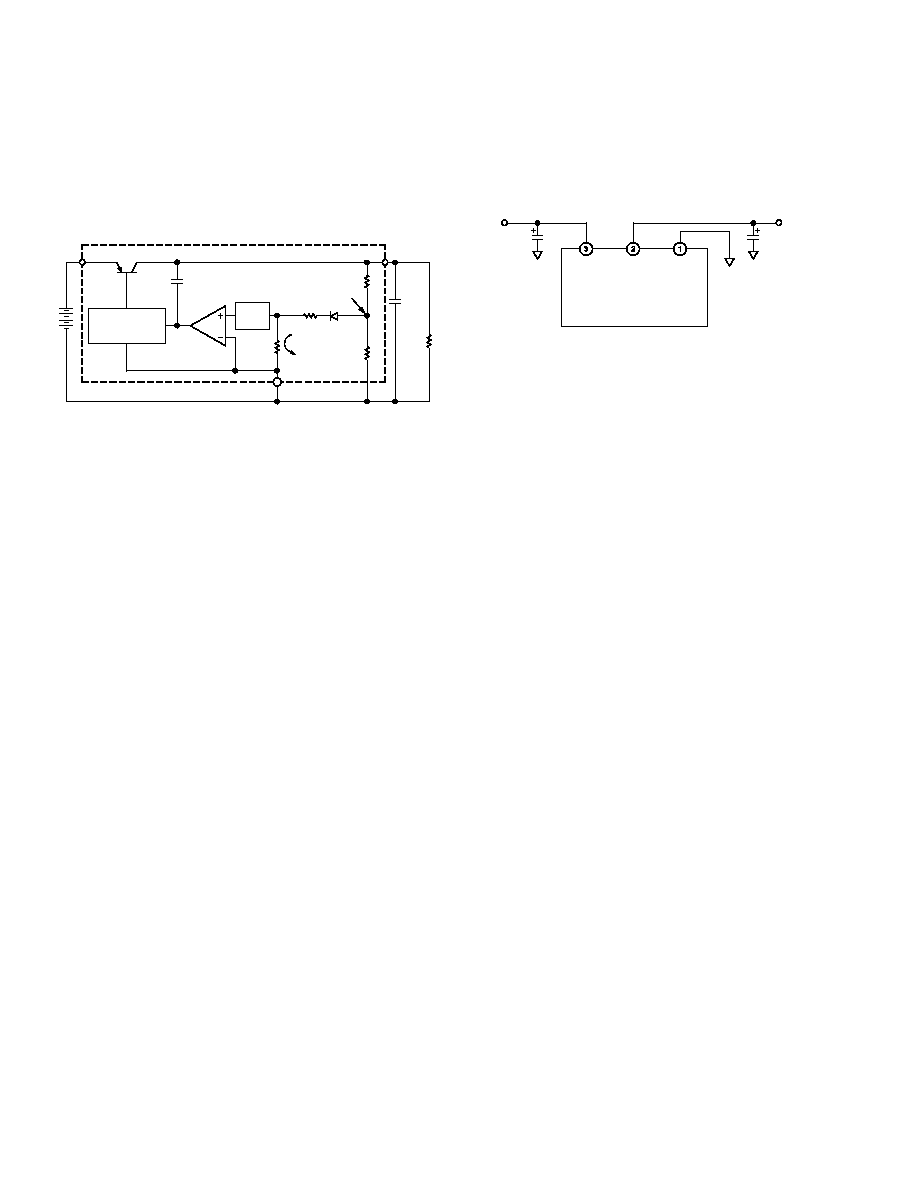
FUNCTIONAL BLOCK DIAGRAM
High-Accuracy Ultralow I
Q
, 1.5 A, anyCAP
®
Low Dropout Regulator
FEATURES
High Accuracy Over Line and Load: 0.9% @ 25 C,
1.5% Over Temperature
Ultralow Dropout Voltage: 230 mV (Typ) @ 1.5 A
Requires Only C
O
= 1.0 F for Stability
anyCAP = Stable with Any Type of Capacitor
(Including MLCC)
Current and Thermal Limiting
Low Noise
2.8 V to 6 V Supply Range
40 C to +85 C Ambient Temperature Range
SOT-223 Package
APPLICATIONS
Notebook, Palmtop Computers
SCSI Terminators
Battery-Powered Systems
PCMCIA Regulator
Bar Code Scanners
Camcorders, Cameras
GENERAL DESCRIPTION
The ADP3339 is a member of the ADP33xx family of precision
low dropout anyCAP voltage regulators. The ADP3339 oper-
ates with an input voltage range of 2.8 V to 6 V and delivers a
load current up to 1.5 A. The ADP3339 stands out from the
conventional LDOs with a novel architecture and an enhanced
process that enables it to offer performance advantages and
higher output current than its competition. Its patented design
requires only a 1.0
µF output capacitor for stability. This device
is insensitive to output capacitor Equivalent Series Resistance
(ESR), and is stable with any good quality capacitor, including
ceramic (MLCC) types for space-restricted applications. The
ADP3339 achieves exceptional accuracy of
±0.9% at room
temperature and
±1.5% over temperature, line and load varia-
tions. The dropout voltage of the ADP3339 is only 230 mV
(typical) at 1.5 A. This device also includes a safety current limit
and thermal overload protection. The ADP3339 has ultralow
quiescent current 130
µA (typical) in light load situations.
anyCAP is a registered trademark of Analog Devices Inc.
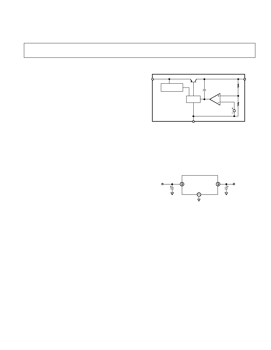
V
IN
OUT
ADP3339
1 F
1 F
V
OUT
GND
IN
Figure 1. Typical Application Circuit
THERMAL
PROTECTION
CC
IN
ADP3339
OUT
R1
R2
GND
Q1
BANDGAP
REF
DRIVER
g
m

REV. 0
2
ADP3339SPECIFICATIONS
1, 2
(V
IN
= 6.0 V, C
IN
= C
OUT
= 1 F, T
J
= 40 C to +125 C unless otherwise noted)
Parameter
Symbol
Conditions
Min
Typ
Max
Unit
OUTPUT
Voltage Accuracy
3
V
OUT
V
IN
= V
OUTNOM
+ 0.5 V to 6 V
0.9
+0.9
%
I
L
= 0.1 mA to 1.5 A
T
J
= 25
°C
V
IN
= V
OUTNOM
+ 0.5 V to 6 V
1.5
+1.5
%
I
L
= 0.1 mA to 1.5 A
T
J
= 40
°C to +125°C
V
IN
= V
OUTNOM
+ 0.5 V to 6 V
1.9
+1.9
%
I
L
= 100 mA to 1.5 A
T
J
= 150
°C
Line Regulation
3
V
IN
= V
OUTNOM
+ 0.5 V to 6 V
0.04
mV/V
T
J
= 25
°C
Load Regulation
I
L
= 0.1 mA to 1.5 A
0.04
mV/mA
T
J
= 25
°C
Dropout Voltage
V
DROP
V
OUT
= 98% of V
OUTNOM
I
L
= 1.5 A
230
480
mV
I
L
= 1 A
180
380
mV
I
L
= 500 mA
150
300
mV
I
L
= 100 mA
100
mV
Peak Load Current
I
LDPK
V
IN
= V
OUTNOM
+ 1 V
2.0
A
Output Noise
V
NOISE
f = 10 Hz100 kHz, C
L
= 10
µF
95
µV rms
I
L
= 1.5 A
GROUND CURRENT
In Regulation
I
GND
I
L
= 1.5 A
13
40
mA
I
L
= 1 A
9
25
mA
I
L
= 500 mA
5
15
mA
I
L
= 100 mA
1
3
mA
I
L
= 0.1 mA
130
200
µA
In Dropout
I
GND
V
IN
= V
OUTNOM
100 mV
100
300
µA
I
L
= 0.1 mA
NOTES
1
All limits at temperature extremes are guaranteed via correlation using standard Statistical Quality Control (SQC) methods.
2
Application stable with no load.
3
V
IN
= 2.8 V for models with V
OUTNOM
2.3 V.
Specifications subject to change without notice.
REV. 0
ADP3339
3
ABSOLUTE MAXIMUM RATINGS
*
Input Supply Voltage . . . . . . . . . . . . . . . . . . . 0.3 V to +8.5 V
Power Dissipation . . . . . . . . . . . . . . . . . . . . Internally Limited
Operating Ambient Temperature Range . . . . 40
°C to +85°C
Operating Junction Temperature Range . . . 40
°C to +150°C
JA
Four-Layer Board . . . . . . . . . . . . . . . . . . . . . . . . 62.3
°C/W
JC
. . . . . . . . . . . . . . . . . . . . . . . . . . . . . . . . . . . . . . 26.8
°C/W
Storage Temperature Range . . . . . . . . . . . . 65
°C to +150°C
Lead Temperature Range (Soldering 10 sec) . . . . . . . . . 300
°C
Vapor Phase (60 sec) . . . . . . . . . . . . . . . . . . . . . . . . . . . 215
°C
Infrared (15 sec) . . . . . . . . . . . . . . . . . . . . . . . . . . . . . . 220
°C
*This is a stress rating only; operation beyond these limits can cause the device
to be permanently damaged. Unless otherwise specified, all voltages are referenced
to GND.
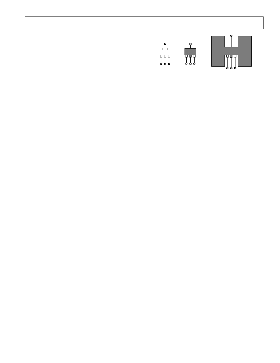
PIN FUNCTION DESCRIPTIONS
Pin
No.
Mnemonic
Function
1
GND
Ground Pin.
2
OUT
Output of the Regulator. Bypass to
ground with a 1
µF or larger capacitor.
3
IN
Regulator Input. Bypass to ground with
a 1
µF or larger capacitor.
PIN CONFIGURATION
TOP VIEW
(Not to Scale)
3
2
1
IN
OUT
ADP3339
OUT
GND
NOTE
PIN 2 AND TAB ARE
INTERNALLY CONNECTED
CAUTION
ESD (electrostatic discharge) sensitive device. Electrostatic charges as high as 4000 V readily
accumulate on the human body and test equipment and can discharge without detection. Although
the ADP3339 features proprietary ESD protection circuitry, permanent damage may occur on
devices subjected to high-energy electrostatic discharges. Therefore, proper ESD precautions are
recommended to avoid performance degradation or loss of functionality.
WARNING!
ESD SENSITIVE DEVICE
ORDERING GUIDE
Output
Package
Package
Model
Voltage
*
Option
Description
ADP3339AKC-1.8
1.8 V
KC (SOT-223)
Plastic Surface Mount
ADP3339AKC-2.5
2.5 V
KC (SOT-223)
Plastic Surface Mount
ADP3339AKC-2.85
2.85 V
KC (SOT-223)
Plastic Surface Mount
ADP3339AKC-3.3
3.3 V
KC (SOT-223)
Plastic Surface Mount
ADP3339AKC-5
5 V
KC (SOT-223)
Plastic Surface Mount
*Contact the factory for other voltage options.
REV. 0
ADP3339
4
Typical Performance Characteristics
(T
A
= 25 C unless otherwise noted.)
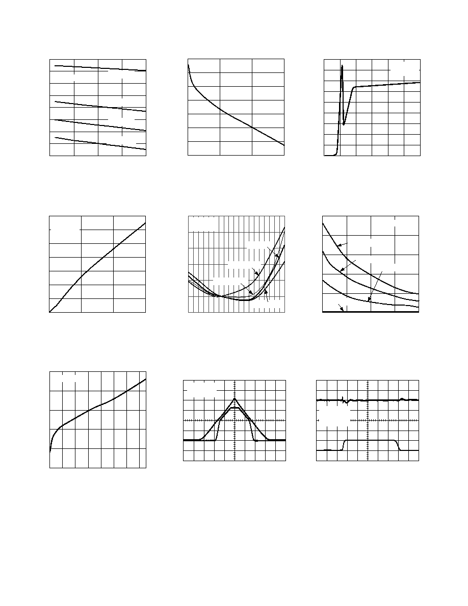
SUPPLY VOLTAGE V
OUTPUT VOLTAGE V
3.301
3
3.300
3.299
3.298
3.297
3.296
3.295
3.294
3.293
4
5
6
7
V
OUT
= 3.3V
I
LOAD
= 0A
I
LOAD
= 1A
I
LOAD
= 1.5A
I
LOAD
= 500mA
TPC 1. Output Voltage vs. Supply
Voltage
LOAD CURRENT A
GROUND CURRENT
mA
14
0
12
10
8
6
4
2
0
0.5
1.0
1.5
V
OUT
= 3.0V
V
IN
= 6V
TPC 4. Ground Current vs.
Load Current
LOAD CURRENT mA
DROPOUT
mV
250
200
150
100
50
0
0
0.2
0.4
0.6
0.8
1.0
1.2
1.4
V
OUT
= 3.3V
TPC 7. Dropout Voltage vs. Load
Current
LOAD CURRENT A
OUTPUT VOLTAGE
V
3.301
0
3.300
3.299
3.298
3.297
3.296
3.295
3.294
0.5
1.0
1.5
V
IN
= 6V
TPC 2. Output Voltage vs. Load
Current
JUNCTION TEMPERATURE C
OUTPUT VOLTAGE
%
1.0
40
0.8
0.6
0.4
0.2
0
0.2
V
IN
= 6V
V
OUT
= 3.3V
20
0
20
40
60
80 100 120 140
I
LOAD
= 10mA
I
LOAD
= 1A
I
LOAD
= 1.5A
I
LOAD
= 500mA
TPC 5. Output Voltage Variation
% vs. Junction Temperature
V
OUT
= 3.3V
I
LOAD
= 1.5A
3
2
1
0
1
2
3
4
5
6
7
8
9
10
TIME s
INPUT/OUTPUT VOLTAGE
V
TPC 8. Power-Up/Power-Down
SUPPLY VOLTAGE V
GROUND CURRENT
A
180
0
160
140
120
60
40
20
0
4
8
12
6
10
2
V
OUT
= 3.3V
I
LOAD
= 0A
100
80
TPC 3. Ground Current
vs. Supply Voltage
JUNCTION TEMPERATURE C
GROUND CURRENT
mA
40
25
20
15
10
5
0
10
60
110
V
OUT
= 3.3V
I
LOAD
= 1A
I
LOAD
= 1.5A
I
LOAD
= 0.5A
I
LOAD
= 1mA
160
TPC 6. Ground Current vs.
Junction Temperature
V
OUT
= 3.3V
I
LOAD
= 1.5A
C
OUT
= 1 F
3.31V
80
120
140
180
TIME s
3.30V
3.29V
5V
4V
40
220
TPC 9. Line Transient Response
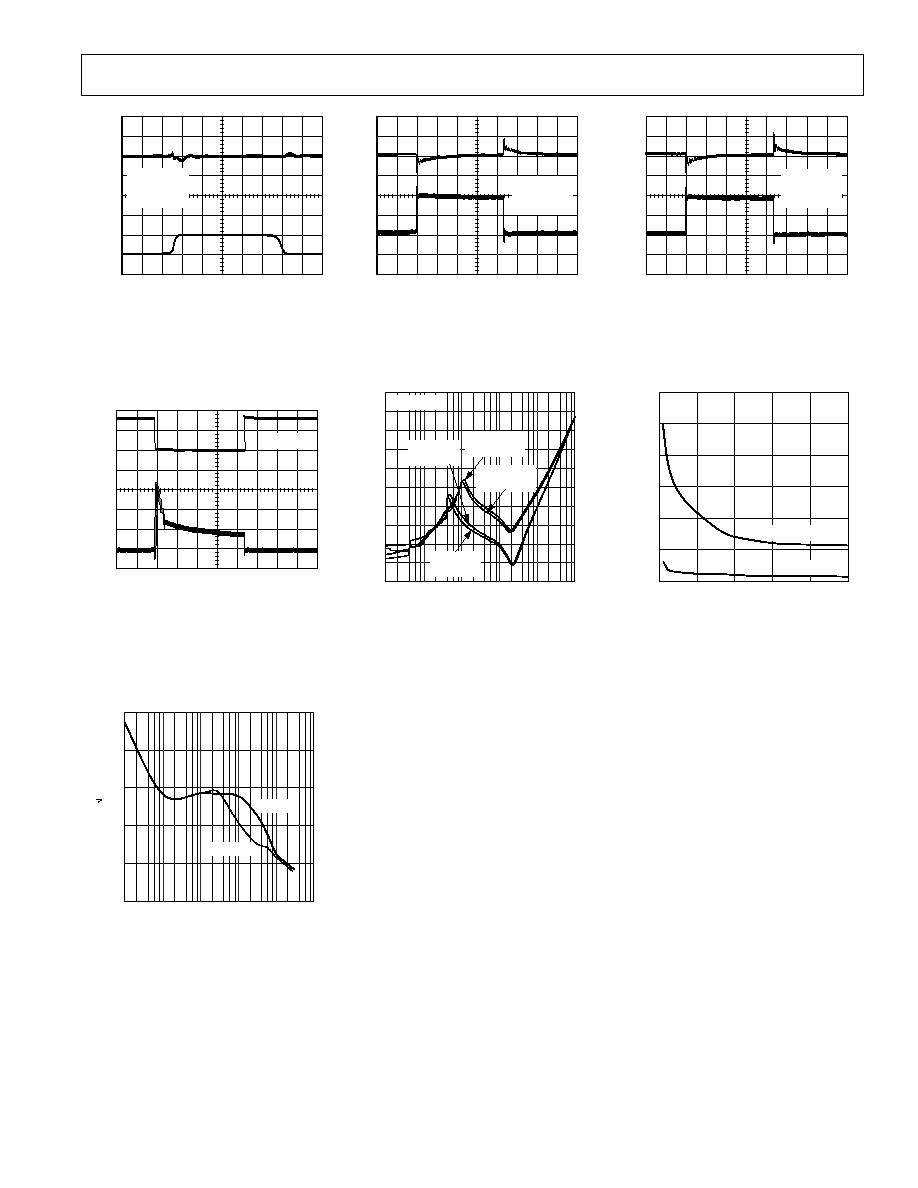
REV. 0
5
ADP3339
V
OUT
= 3.3V
I
LOAD
= 1.5A
C
OUT
= 10 F
3.31V
80
120
140
180
TIME s
3.30V
3.29V
5V
4V
220
40
TPC 10. Line Transient Response
200
400
600
800
TIME s
3.3V
0
1A
0
3A
2A
V
IN
= 6V
TPC 13. Short-Circuit Current
FREQUENCY Hz
10
100
10
1
0.1
0.01
0.001
100
1k
10k
100k
1M
C
L
= 1 F
C
L
= 10 F
VOLTAGE NOISE SPECTRAL DENSITY
V/
Hz
TPC 16. Output Noise Density
V
IN
= 6V
C
OUT
= 10 F
I
LOAD
= 1.5A
3.5V
200
400
600
800
3.3V
3.1V
0.5A
0
1.5A
1.0A
0
1000
TIME s
TPC 11. Load Transient Response
START 10.000Hz
10
0
10
20
30
40
50
60
70
80
90
100
100
1k
10k
100k
1M
STOP 100,000.000Hz
V
OUT
= 3.3V
C
L
= 10 F
I
LOAD
= 1.5A
C
L
= 1 F
I
LOAD
= 1.5A
C
L
= 10 F
I
LOAD
= 0A
C
L
= 1 F
I
LOAD
= 0A
RIPPLE REJECTION
dB
FREQUENCY Hz
TPC 14. Power Supply Ripple
Rejection
200
400
600
800
TIME s
3.5V
3.3V
3.1V
0.5A
0
1.5A
1.0A
0
1000
V
IN
= 6V
C
OUT
= 1 F
I
LOAD
= 1.5A
TPC 12. Load Transient Response
C
L
F
RMS NOISE
V
600
0
500
400
300
200
100
0
10
20
30
40
I
LOAD
= 0A
I
LOAD
= 1.5A
50
TPC 15. RMS Noise vs. C
L
(10 Hz100 kHz)
REV. 0
ADP3339
6
THEORY OF OPERATION
The new anyCAP
LDO ADP3339 uses a single control loop for
regulation and reference functions. The output voltage is sensed
by a resistive voltage divider consisting of R1 and R2 which is
varied to provide the available output voltage option. Feedback
is taken from this network by way of a series diode (D1) and a
second resistor divider (R3 and R4) to the input of an amplifier.
PTAT
V
OS
g
m
NONINVERTING
WIDEBAND
DRIVER
INPUT
Q1
ADP3339
COMPENSATION
CAPACITOR
ATTENUATION
(V
BANDGAP
/V
OUT
)
R1
D1
R2
R3
R4
OUTPUT
PTAT
CURRENT
(a)
GND
C
LOAD
R
LOAD
Figure 2. Functional Block Diagram
A very high-gain error amplifier is used to control this loop. The
amplifier is constructed in such a way that equilibrium pro-
duces a large, temperature-proportional input, "offset voltage"
that is repeatable and very well controlled. The temperature-
proportional offset voltage is combined with the complementary
diode voltage to form a "virtual bandgap" voltage, implicit in
the network, although it never appears explicitly in the circuit.
Ultimately, this patented design makes it possible to control
the loop with only one amplifier. This technique also improves
the noise characteristics of the amplifier by providing more flexibil-
ity on the trade-off of noise sources that leads to a low noise design.
The R1, R2 divider is chosen in the same ratio as the bandgap
voltage to the output voltage. Although the R1, R2 resistor divider
is loaded by the diode D1 and a second divider consisting of R3
and R4, the values can be chosen to produce a temperature-stable
output. This unique arrangement specifically corrects for the load-
ing of the divider, thus avoiding the error resulting from base
current loading in conventional circuits.
The patented amplifier controls a new and unique noninverting
driver that drives the pass transistor, Q1. The use of this special
noninverting driver enables the frequency compensation to
include the load capacitor in a pole-splitting arrangement to
achieve reduced sensitivity to the value, type, and ESR of the
load capacitance.
Most LDOs place very strict requirements on the range of ESR
values for the output capacitor because they are difficult to stabilize
due to the uncertainty of load capacitance and resistance. More-
over, the ESR value, required to keep conventional LDOs stable,
changes depending on load and temperature. These ESR limita-
tions make designing with LDOs more difficult because of their
unclear specifications and extreme variations over temperature.
With the ADP3339 anyCAP LDO, this is no longer true. It
can be used with virtually any good quality capacitor, with no
constraint on the minimum ESR. This innovative design allows
the circuit to be stable with just a small 1
µF capacitor on the out-
put. Additional advantages of the pole-splitting scheme include
superior line noise rejection and very high regulator gain, which
leads to excellent line and load regulation. An impressive
±1.5
accuracy is guaranteed over line, load, and temperature.
Additional features of the circuit include current limit and ther-
mal shutdown.
V
IN
OUT
ADP3339
C1
1 F
C2
1 F
V
OUT
GND
IN
Figure 3. Typical Application Circuit
A
PPLICATION INFORMATION
CAPACITOR SELECTION
Output Capacitor
The stability and transient response of the LDO is a function of
the output capacitor. The ADP3339 is stable with a wide range
of capacitor values, types, and ESR (anyCAP). A capacitor as
low as 1
µF is all that is needed for stability. A higher capacitance
may be necessary if high output current surges are anticipated or
if the output capacitor cannot be located near the output and
ground pins. The ADP3339 is stable with extremely low ESR
capacitors (ESR 0), such as Multilayer Ceramic Capacitors
(MLCC) or OSCON. Note that the effective capacitance of
some capacitor types fall below the minimum over temperature
or with dc voltage.
Input Capacitor
An input bypass capacitor is not strictly required but it is recom-
mended in any application involving long input wires or high
source impedance. Connecting a 1
µF capacitor from the
input to ground reduces the circuit's sensitivity to PC board
layout and input transients. If a larger output capacitor is neces-
sary, then a larger value input capacitor is also recommended.
OUTPUT CURRENT LIMIT
The ADP3339 is short-circuit protected by limiting the pass
transistor's base drive current. The maximum output current is
limited to about 3 A, see TPC 13.
THERMAL OVERLOAD PROTECTION
The ADP3339 is protected against damage due to excessive power
dissipation by its thermal overload protection circuit. Thermal
protection limits the die temperature to a maximum of 160
°C.
Under extreme conditions (i.e., high ambient temperature and
power dissipation) where the die temperature starts to rise above
160
°C, the output current will be reduced until the die tempera-
ture has dropped to a safe level.
Current and thermal limit protections are intended to protect
the device against accidental overload conditions. For normal
operation, the device's power dissipation should be externally
limited so that the junction temperature will not exceed 125
°C.
REV. 0
ADP3339
7
CALCULATING POWER DISSIPATION
Device power dissipation is calculated as follows:
P
V
V
I
V
I
D
IN
OUT
LOAD
IN
GND
=
-
(
)
×
+
( )
×
Where I
LOAD
and I
GND
are load current and ground current, V
IN
and V
OUT
are the input and output voltages respectively.
Assuming worst-case operating conditions are I
LOAD
= 1.5 A,
I
GND
= 14 mA, V
IN
= 3.3 V, and V
OUT
= 2.5 V, the device power
dissipation is:
P
V
V
mA
V
mA
mW
D
=
(
)
+
(
)
=
3 3
2 5
1500
3 3
14
1246
.
.
.
So, for a maximum junction temperature of 125
°C and a
maximum ambient temperature of 85
°C, the required ther-
mal resistance from junction to ambient is:
JA
C
C
W
C W
=
° - ° =
°
125
85
1 246
32 1
.
.
/
PRINTED CIRCUIT BOARD LAYOUT
CONSIDERATIONS
The SOT-223's thermal resistance,
JA
, is determined by the
sum of the junction-to-case and the case-to-ambient thermal
resistances. The junction-to-case thermal resistance,
JC
, is
determined by the package design and specified at 26.8
°C/W.
However, the case-to-ambient thermal resistance is determined
by the printed circuit board design.
As shown in Figures 4a4c, the amount of copper to which the
ADP3339 is mounted affects the thermal performance. When
mounted to just the minimal pads of 2 oz. copper (Figure 4a),
the
JA
is 126.6
°C/W. By adding a small copper pad under the
ADP3339 (Figure 4b), reduces the
JA
to 102.9
°C/W. Increasing
the copper pad to 1 square inch (Figure 4c), reduces the
JA
even further to 52.8
°C/W.
a.
b.
c.
Figure 4. PCB Layouts
Use the following general guidelines when designing printed
circuit boards:
1. Keep the output capacitor as close to the output and ground
pins as possible.
2. Keep the input capacitor as close to the input and ground
pins as possible.
3. PC board traces with larger cross sectional areas will remove
more heat from the ADP3339. For optimum heat transfer,
specify thick copper and use wide traces.
4. The thermal resistance can be decreased by adding a copper
pad under the ADP3339 as shown in Figure 4b.
5. If possible, utilize the adjacent area to add more copper
around the ADP3339. Connecting the copper area to the
output of the ADP3339, as shown in Figure 4c, is best but
will improve thermal performance even if it is connected to
other pins.
6. Use additional copper layers or planes to reduce the thermal
resistance. Again, connecting the other layers to the output
of the ADP3339 is best, but not necessary. When connecting
the output pad to other layers use multiple vias.
REV. 0
8
C02191110/01(0)
PRINTED IN U.S.A.
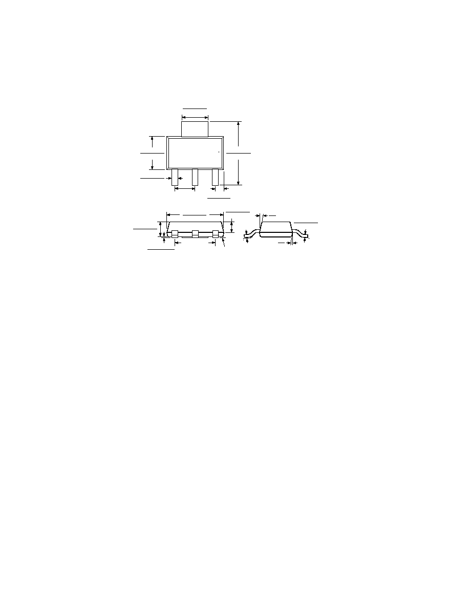
ADP3339
OUTLINE DIMENSIONS
Dimensions shown in inches and (mm).
3-Lead Surface Mount
KC (SOT-223)
SEATING
PLANE
0.051 (1.30)
0.043 (1.10)
0.264 (6.70)
0.248 (6.30)
0.067 (1.70)
0.060 (1.50)
0.004 (0.10)
0.0008 (0.02)
0.181 (4.60)
NOM
10
MAX
0.25 (0.35)
0.010 (0.25)
16
10
16
10
1
3
2
4
0.124 (3.15)
0.116 (2.95)
0.146 (3.70)
0.130 (3.30)
0.287 (7.30)
0.264 (6.70)
0.0905 (2.30)
NOM
0.041 (1.05)
0.033 (0.85)
0.033 (0.85)
0.026 (0.65)
Document Outline
- Specifications
- Pinout
- Package Drawings
- Ordering Guide
- Features
- Applications
- Product Description
- Absolute Maximum Ratings
- Functional Block Diagram
- Pin Function Description
- Circuit Description
- Typical Characteristics
- CAUTION
- THEORY OF OPERATION
- APPLICATION INFORMATION
- OUTPUT CURRENT LIMIT
- THERMAL OVERLOAD PROTECTION
- CALCULATING POWER DISSIPATION
- PRINTED CIRCUIT BOARD LAYOUT CONSIDERATIONS
- DIAGRAMS
- Typical Application Circuit
- Functional Block Diagram
- Typical Application Circuit
- PCB Layouts