 | ÐлекÑÑоннÑй компоненÑ: ADP3342 | СкаÑаÑÑ:  PDF PDF  ZIP ZIP |
Äîêóìåíòàöèÿ è îïèñàíèÿ www.docs.chipfind.ru
REV. 0
Information furnished by Analog Devices is believed to be accurate and
reliable. However, no responsibility is assumed by Analog Devices for its
use, nor for any infringements of patents or other rights of third parties that
may result from its use. No license is granted by implication or otherwise
under any patent or patent rights of Analog Devices.
a
ADP3342
One Technology Way, P.O. Box 9106, Norwood, MA 02062-9106, U.S.A.
Tel: 781/329-4700
www.analog.com
Fax: 781/326-8703
© Analog Devices, Inc., 2002
Ultralow, I
Q
, anyCAP
®
Low Dropout Regulator
FEATURES
Accuracy Over Line and Load: 4.0% @ 25 C,
5% Over Temperature
Ultralow Dropout Voltage: 300 mV (Typ) @ 300 mA
Requires Only C
O
= 1.0 F for Stability
anyCAP = Stable with any Type of Capacitor
(including MLCC)
Current and Thermal Limiting
Low Shutdown Current: < 2 A
1.7 V V
IN
6 V
2.8 V VCC 6 V
V
OUT
= 1.2 V 5%
40 C to +100 C Ambient Temperature Range
Ultrasmall Thermally Enhanced 8-Lead MSOP Package
APPLICATIONS
Notebook PCs
Desktop PCs
GENERAL DESCRIPTION
The ADP3342 is a unique member of the ADP330x family of
precision low dropout anyCAP voltage regulators. The ADP3342
operates with an input voltage range of 1.7 V to 6 V and delivers
a continuous load current up to 300 mA. In order to support the
ability to regulate from such a low input voltage, the power rail
to the IC, VCC, has been split off from the main power rail, V
IN
,
from which the output is powered.
The ADP3342 stands out from the conventional LDOs with the
lowest thermal resistance of any MSOP-8 package and an enhanced
process that enables it to offer performance advantages beyond
its competition. Its patented design requires only a 1.0
µF output
capacitor for stability. This device is insensitive to output capacitor
Equivalent Series Resistance (ESR), and is stable with any good
quality capacitor, including ceramic (MLCC) types for space-
restricted applications. The dropout voltage of the ADP3342 is
only 190 mV (typical) at 300 mA. This device also includes a
safety current limit, thermal overload protection and a shutdown
control pin.
FUNCTIONAL BLOCK DIAGRAM
THERMAL
PROTECTION
CC
IN
ADP3342
OUT
GND
Q1
g
m
BANDGAP +
REF
DRIVER
VCC
PWRGD
SD
+
VCC
IN
IN
SD
OUT
OUT
PWRGD
GND
ADP3342
+
ON
OFF
1 F
V
IN
1.8V
1 F
V
OUT
1.2V
3.3V
Figure 1. Typical Application Circuit
anyCAP
is a registered trademark of Analog Devices, Inc.

REV. 0
2
ADP3342SPECIFICATIONS
(VCC = 3.0 V, V
IN
= 1.8 V, C
IN
= C
OUT
= 1 F, T
A
= 0 C to 100 C and T
A
= 40 C to
+100 C, unless otherwise noted.)
Parameter
Symbol
Conditions
Min
Typ
Max
Unit
OUTPUT
Voltage Accuracy
V
OUT
VCC = 2.8 V to 6 V, V
IN
= 1.7 V to 6 V
4.0
+4.0
%
I
L
= 0.1 mA to 300 mA
T
A
= 25
°C
VCC = 2.8 V to 6 V, V
IN
= 1.7 V to 6 V
5.0
+5.0
%
I
L
= 0.1 mA to 300 mA,
T
A
= 40
°C to +100°C
Line Regulation
VCC = 2.8 V to 6 V, V
IN
= 1.7 V to 6 V
0.04
mV/V
T
A
= 25
°C
Load Regulation
I
L
= 0.1 mA to 300 mA
0.12
mV/mA
T
A
= 25
°C
Dropout Voltage
V
DROP
V
OUT
= 98% of V
OUTNOM
I
L
= 300 mA
190
450
mV
I
L
= 200 mA
125
mV
I
L
= 100 mA
70
mV
Current Limiting
I
LIM
VCC = 3 V, V
IN
= 1.8 V
450
mA
Output Noise
V
NOISE
f = 10 Hz100 kHz, C
L
= 1
µF
60
µV rms
I
L
= 300 mA
OPERATING CURRENTS
Ground Current in Regulation
I
GND
I
L
= 300 mA, T
A
= 40
°C to +100°C
3.0
8.5
mA
I
L
= 300 mA, T
A
= 0
°C to 100°C
3.0
6.0
mA
I
L
= 300 mA, T
A
= 25
°C
3.0
4.0
mA
I
L
= 200 mA
2.0
mA
I
L
= 0.1 mA
100
175
µA
VCC Current in Regulation
IVCC
I
L
= 300 mA
100
170
µA
Ground Current in Shutdown
I
GNDSD
SD = 0 V, VCC = 6 V, V
IN
= 1.8 V
0.01
2
µA
SHUTDOWN
Threshold Voltage
V
THSD
ON
VCC 0.9
V
OFF
0.6
V
SD Input Current
I
SD
0
SD 6 V
1.4
7
µA
Output Current In Shutdown
I
OSD
T
A
= 25
°C VCC = 6 V, V
IN
= 6 V
0.01
1
µA
T
A
= 100
°C VCC = 6 V, V
IN
= 6 V
0.01
2
µA
PWRGD
Power Good Output Voltage
I
PWRGDL
V
PWRGD
= 1.2 V, VCC = 3.0 V
0.85
1.5
mA
V
PWRGDL
2
I
PWRGD
= 300
µA
0.4
V
V
PWRGDH
2
I
PWRGD
= 300
µA
VCC 0.4
V
Power Good On Time Delay
TD1
3
I
L
= 3 mA to 300 mA,
5
300
µs
C
OUT
= 1
µF to 10 µF
TD2
4
I
L
= 3 mA to 300 mA,
50
300
µs
C
OUT
= 1
µF to 10 µF
Power Good Off Time Delay
TD3
5
I
L
= 3 mA to 300 mA,
0.05
1
µs
C
OUT
= 1
µF to 10 µF
THERMAL PROTECTION
Shutdown Temperature
TH
PROT
I
L
= 100 mA
165
°C
NOTES
1
Ambient temperature of 100
°C corresponds to a junction temperature of 125°C under typical full load test conditions.
2
V
PWRGDL
, V
PWRGDH
,: Powergood output voltages. Guaranteed by design and characterization.
3
TD1: Delay time from V
OUT
crossing 1 V to PWRGD high. Guaranteed by design.
4
TD2: Delay time from
SD high to PWRGD high. Guaranteed by design.
5
TD3: Delay time between
SD low to PWRGD low. Guaranteed by design.
Specifications subject to change without notice.
REV. 0
ADP3342
3
PIN CONFIGURATION
TOP VIEW
(Not to Scale)
8
7
6
5
1
2
3
4
VCC
OUT
OUT
GND
IN
ADP3342
SD
PWRGD
IN
PIN FUNCTION DESCRIPTIONS
Pin No.
Mnemonic
Function
1, 2
OUT
Output of the Regulator. Bypass to ground with a 1.0
µF or larger capacitor. All pins must be
connected together for proper operation.
3
VCC
Supply Voltage
4
GND
Ground Pin
5
PWRGD
Power Good. Used to indicate output is in regulation.
6
SD
Active Low Shutdown Pin. Connect to ground to disable the regulator output. When shut down
is not used, this pin should be connected to the input pin.
7, 8
IN
Regulator Input. All pins must be connected together for proper operation.
CAUTION
ESD (electrostatic discharge) sensitive device. Electrostatic charges as high as 4000 V readily
accumulate on the human body and test equipment and can discharge without detection. Although
the ADP3342 features proprietary ESD protection circuitry, permanent damage may occur on
devices subjected to high-energy electrostatic discharges. Therefore, proper ESD precautions are
recommended to avoid performance degradation or loss of functionality.
WARNING!
ESD SENSITIVE DEVICE
ABSOLUTE MAXIMUM RATINGS
*
Input Supply Voltage . . . . . . . . . . . . . . . . . . . 0.3 V to +13 V
Shutdown Input Voltage . . . . . . . . . . . . . . . . 0.3 V to +13 V
Power Dissipation . . . . . . . . . . . . . . . . . . . Internally Limited
Operating Ambient Temperature Range . . . 40
°C to +100°C
Operating Junction Temperature Range . . . 40
°C to +125°C
JA
(2-layer) . . . . . . . . . . . . . . . . . . . . . . . . . . . . . . . 157
°C/W
JA
(4-layer) . . . . . . . . . . . . . . . . . . . . . . . . . . . . . . . 121
°C/W
JC
. . . . . . . . . . . . . . . . . . . . . . . . . . . . . . . . . . . . . . . 56
°C/W
Storage Temperature Range . . . . . . . . . . . . 65
°C to +150°C
Lead Temperature Range (Soldering 10 sec) . . . . . . . . 300
°C
Vapor Phase (60 sec) . . . . . . . . . . . . . . . . . . . . . . . . . . 215
°C
Infrared (15 sec) . . . . . . . . . . . . . . . . . . . . . . . . . . . . . 220
°C
*This is a stress rating only; operation beyond these limits can cause the device
to be permanently damaged.
ORDERING GUIDE
Model
Output Voltage
*
Package Option
Marking Code
Temperature Range
ADP3342JRM-REEL7
1.2 V
RM-8 (MSOP-8)
LJA
0
°C to 100°C
ADP3342ARM-REEL7 1.2 V
RM-8 (MSOP-8)
LJB
40
°C to +100°C
*Contact the factory for other output voltage options.
REV. 0
ADP3342
4
INPUT VOLTAGE V
OUTPUT V
O
L
T
A
GE
V
1.7
2.7
3.7
4.7
5.7
1.17
1.18
1.19
1.20
1.21
1.22
1.23
1.24
1.25
V
OUT
= 1.2V
V
CC
= 3V
I
L
= 100mA
I
L
= 300mA
I
L
= 200mA
I
L
= 0mA
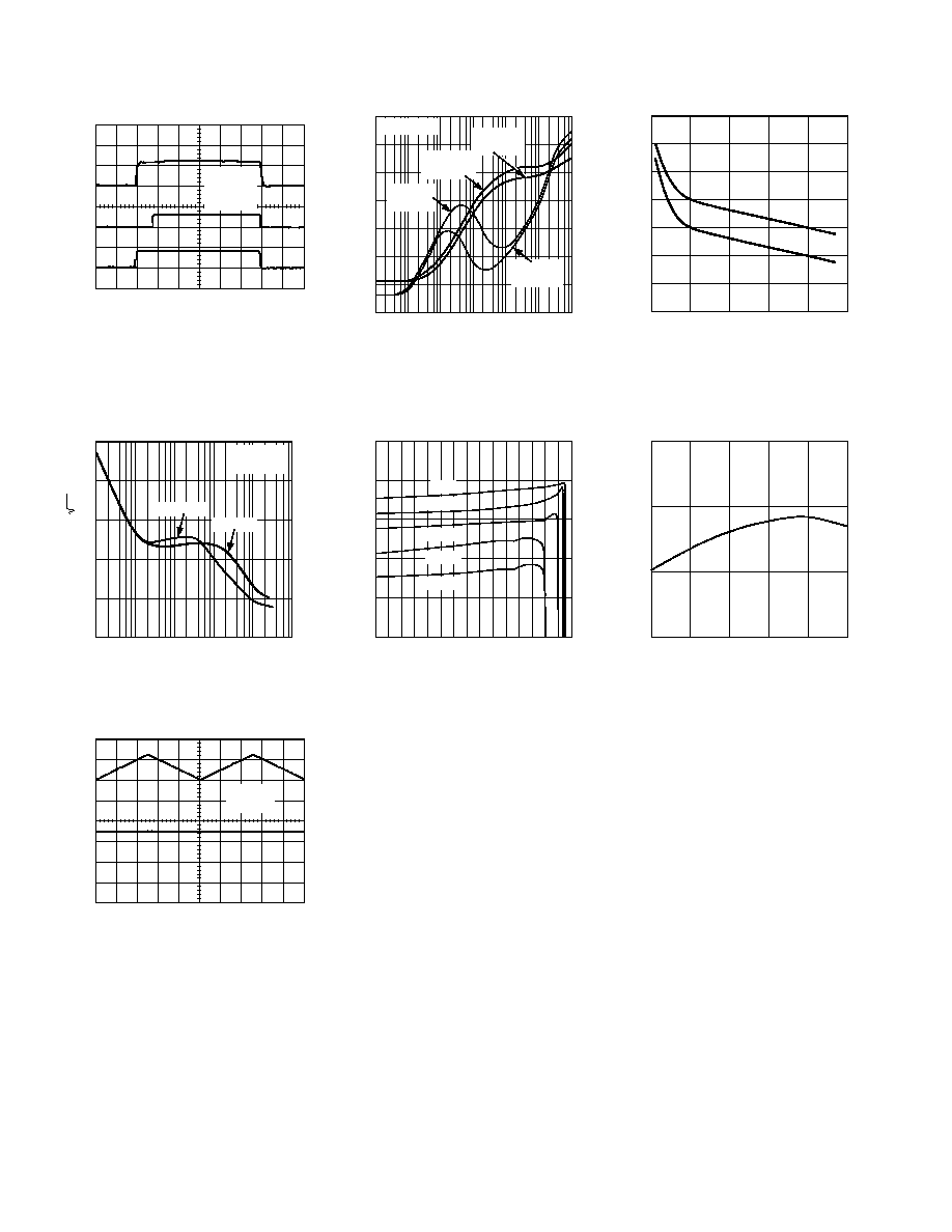
TPC 1. Line Regulation Output Voltage
vs. Supply Voltage
OUTPUT LOAD mA
GROUND CURRENT
mA
3.5
0
50
100
150
200
250
300
3.0
2.5
2.0
1.5
1.0
0
0.5
V
IN
= 1.8V
V
CC
= 3.0V
TPC 4. Ground Current vs. Load Current
OUTPUT LOAD mA
INPUT-OUTPUT VOLTAGE
V
0.25
0
50
100
200
250
150
300
0.20
0.15
0.10
0.05
0
TPC 7. Dropout Voltage vs. Output
Current
Typical Performance Characteristics
OUTPUT LOAD mA
OUTPUT VOLTAGE
V
0
50
100
150
200
250
300
1.23
1.22
1.21
1.20
1.19
1.18
1.17
V
IN
= 1.8V
V
CC
= 3.0V
TPC 2. Output Voltage vs. Load Current
JUNCTION TEMPERATURE C
OUTPUT CHANNEL
%
1.0
0.3
50 25
150
0
25
50
75
100
125
0.9
0.7
0.6
0.5
0.4
0.8
0.2
0.1
0
0.1
0.2
0.3
0.4
0
200mA
300mA
TPC 5. Output Voltage Variation
vs. Junction Temperature
TEMPERATURE C
GROUND CURRENT @ 300mA LOAD
mA
7.0
6.5
6.0
5.5
5.0
4.5
40 25 10
5
20
35
50
65
80
0
4.0
3.5
3.0
2.5
2.0
1.5
1.0
V
CC
= 3.0V
V
IN
= 1.8V
95
MAX
TYP
MIN
TPC 8. Ground Current @ 300 mA
Load vs. Ambient Temperature
INPUT VOLTAGE V
GROUND CURRENT
A
120
110
100
90
1.2 1.6 2.0 2.4 2.8 3.2 3.6 4.0 4.4 4.8 5.2 5.6 6.0
80
70
60
50
V
OUT
= 1.2V
V
CC
= 3V
I
L
= 0 A
TPC 3. Ground Current vs. Supply
Voltage
JUNCTION TEMPERATURE C
GROUND CURRENT
mA
5.50
40
20
0
20
40
60
80
100
5.00
4.50
4.00
3.50
3.00
2.50
2.00
1.50
1.00
0.50
0
V
CC
= 3.0V
V
IN
= 1.8V
I
L
= 0mA
I
L
= 100mA
I
L
= 200mA
I
L
= 300mA
TPC 6. Ground Current vs. Junction
Temperature
TIME s
200
400
600
800
V
OUT
= 1.2V
SD = V
IN
R
L
= 4
INPUT/OUTPUT VOLTAGE
V
4
3
2
1
0
0
1000
1
2
5
6
TPC 9. Power-Up/Power-Down
REV. 0
5
ADP3342
TIME s
40
80
120
160
1.32
1.22
1.12
3.00
1.80
V
CC
= 3V
C
L
= 1 F
R
L
= 4
V
IN
VV
OUT
V
0
200
TPC 10. Line Transient Response
TIME s
400
1200
800
1.3
1.2
1.1
200
5
V
CC
= 3V
V
IN
= 1.8V
C
L
= 10 F
400
0
mA
VOLTS
0
1600
2000
TPC 13. Load Transient Response
TIME s
100
200
300
400
2.0
1.0
0
3.0
0
1.8
0
V
CC
= 3V
V
IN
= 1.8V
R
L
= 4
SD
V
OUTPUT
V
PWRGD
V
0
500
TPC 16. Turn On Delay
TIME s
40
80
120
160
1.32
1.22
1.12
3.00
1.80
V
CC
= 3V
C
L
= 10 F
R
L
= 4
V
IN
VV
OUT
V
0
200
TPC 11. Line Transient Response
TIME s
200
400
600
800
1.2
0
1.0
0.5
0
V
IN
= 1.8V
A
V
OLTS
0
1000
TPC 14. Short Circuit Current
TIME s
6
10
14
18
2.0
1.0
0
3.0
0
1.8
0
V
CC
= 3V
V
IN
= 1.8V
R
L
= 4
2
SD
V
OUTPUT
V
PWRGD
V
TPC 17. Turn Off Delay
TIME s
400
1200
800
1.3
1.2
1.1
200
5
V
CC
= 3V
V
IN
= 1.8V
C
L
= 1 F
400
0
mA
VOLTS
0
1600
2000
TPC 12. Load Transient Response
TIME s
200
600
1000
1400
2.0
1.0
0
3.0
0
1.8
0
V
CC
= 3V
R
L
= 4
V
IN
= 1.8V
SD
V
OUTPUT
V
PWRGD
V
200
1800
TPC 15. Power-On/Power-Off
Response from Shutdown
TIME s
200
600
1000
1400
2.0
1.0
0
3.0
0
V
CC
V
OUTPUT
V
V
IN
= 1.8V
SD = 3.0V
R
L
= 4
1800
TPC 18. Power-On/Power-Off
Response from V
CC
REV. 0
ADP3342
6
TIME s
200
400
600
800
1.2
0
3.0
0
1.8
0
V
IN
= 1.8V
SD = 3.0V
R
L
= 4
V
IN
V
OUTPUT
V
PWRGD
V
0
1000
TPC 19. Power On/Power Off
Response from V
IN
FREQUENCY Hz
VOLTAGE NOISE SPECTRAL
DENSITY
V/ Hz
100
10
10
1
0.1
0.01
0.001
100
1k
10k
100k
1M
C
L
= 10 F
C
L
= 1 F
V
OUT
= 1.2V
I
L
= 1mA
TPC 22. Output Noise Density
TIME ms
5
25
35
45
3.6
3.0
400
200
0
V
IN
= 1.8V
SD = 3V
15
V
CC
V
mA
TPC 25. Current Limiting from V
CC
FREQUENCY Hz
RIPPLE REJECTION
dB
10
100
1k
10k
100k
1M
10M
20
30
40
50
60
70
80
90
V
OUT
= 1.2V
C
L
= 1 F
I
L
= 50 A
C
L
= 1 F
I
L
= 300mA
C
L
= 10 F
I
L
= 300mA
C
L
= 10 F
I
L
= 50 A
TPC 20. Power Supply Ripple
Rejection
AMBIENT TEMPERATURE C
OUTPUT VOLTAGE
V
1.25
1.23
1.21
1.19
1.17
1.15
0mA
50mA
100mA
200mA
300mA
35
55
75
95
115
135
155
175
TPC 23. Thermal Protection
C
L
F
RMS NOISE
V
70
0
10
20
30
40
50
60
50
40
20
10
0
30
300mA
0mA
TPC 21. RMS Noise vs. C
L
(10 Hz100 Hz)
V
IN
V
1.5
1.7
1.8
2.0
650
600
550
500
1.6
I
CL
mA
1.9
TPC 24. Current Limit vs. V
IN
REV. 0
ADP3342
7
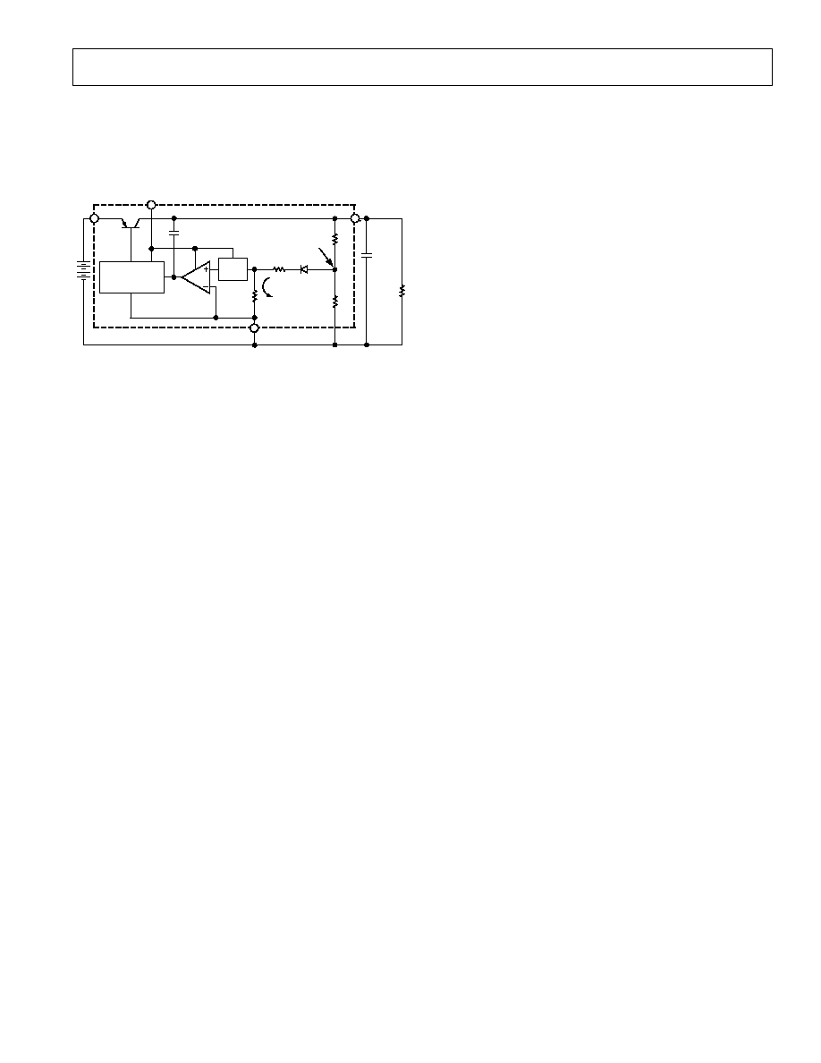
THEORY OF OPERATION
The new anyCAP LDO ADP3342 uses a single control loop for
regulation and reference functions. The output voltage is sensed
by a resistive voltage divider consisting of R1 and R2. Feedback
is taken from this network by way of a series diode (D1) and a
second resistor divider (R3 and R4) to the input of an amplifier.
PTAT
V
OS
NONINVERTING
WIDEBAND
DRIVER
INPUT
Q1
ADP3342
COMPENSATION
CAPACITOR
ATTENUATION
(V
BANDGA P
/V
OUT
)
R1
D1
R2
R3
R4
OUTPUT
PTAT
CURRENT
(a)
C
LOAD
R
LOAD
GND
g
m
VCC
Figure 2. Control Loop Functional Block Diagram
A very high gain error amplifier is used to control this loop. The
amplifier is constructed in such a way that at equilibrium it
produces a large, temperature proportional input "offset voltage"
that is repeatable and very well controlled. The temperature
proportional offset voltage is combined with the complementary
diode voltage to form a "virtual bandgap" voltage, implicit in
the network, although it never appears explicitly in the circuit.
Ultimately, this patented design makes it possible to control the
loop with only one amplifier. This technique also improves the
noise characteristics of the amplifier by providing more flexibility
on the trade-off of noise sources that leads to a low noise design.
The R1, R2 divider is chosen in the same ratio as the bandgap
voltage to the output voltage. Although the R1, R2 resistor
divider is loaded by the diode D1 and a second divider consisting
of R3 and R4, the values can be chosen to produce a temperature
stable output. This unique arrangement specifically corrects for
the loading of the divider so that the error resulting from base
current loading in conventional circuits is avoided.
The patented amplifier controls a new and unique noninverting
driver that drives the pass transistor, Q1. The use of this special
noninverting driver enables the frequency compensation to include
the load capacitor in a pole splitting arrangement to achieve reduced
sensitivity to the value, type and ESR of the load capacitance.
Most LDOs place very strict requirements on the range of ESR
values for the output capacitor because they are difficult to stabilize
due to the uncertainty of load capacitance and resistance. More-
over, the ESR value, required to keep conventional LDOs stable,
changes depending on load and temperature. These ESR limitations
make designing with LDOs more difficult because of their unclear
specifications and extreme variations over temperature.
With the ADP3342 anyCAP LDO, this is no longer true. It can
be used with virtually any good quality capacitor, with no con-
straint on the minimum ESR. This innovative design allows the
circuit to be stable with just a small 1
µF capacitor on the output.
Additional advantages of the pole splitting scheme include superior
line noise rejection and very high regulator gain which leads to
excellent line and load regulation.
Additional features of the circuit include current limit and thermal
shutdown and noise reduction.
APPLICATION INFORMATION
PC Application--VCCVID
The ADP3342 has been optimized for PC applications that
require a 1.2 V output for powering the voltage identification
rail, VCCVID. The rail from which the output draws current,
the IN pin, is separated from the rail that powers the IC, the
VCC pin. This allows a higher efficiency design when, as
recommended for the IMVP-3 application, the VCC pin is
connected to a 3.3 V supply to power the IC adequately, and
the IN pin is connected to a 1.8 V supply. The efficiency is
nearly 60% in this case.
Capacitor Selection
As with any voltage regulator, output transient response is a
function of the output capacitance. The ADP3342 is stable with
a wide range of capacitor values, types and ESR (anyCAP).
A capacitor as low as 1
µF is all that is needed for stability; larger
capacitors can be used if high output current surges are anticipated.
The ADP3342 is stable with extremely low ESR capacitors (ESR
0),
such as multilayer ceramic capacitors (MLCC) or OSCON.
Note that the effective capacitance of some capacitor types may
fall below the minimum at cold temperature. Ensure that the
capacitor provides more than 1
µF at minimum temperature.
Input Bypass Capacitor
An input bypass capacitor is not strictly required but is advisable
in any application involving long input wires or high source
impedance. Connecting a 1
µF capacitor from IN to ground reduces
the circuit's sensitivity to PC board layout. If a larger value output
capacitor is used, then a larger value input capacitor is also
recommended.
Power Good Monitoring Function
The PWRGD pin does not monitor the output voltage directly,
but rather detects whether the internal PNP pass transistor is being
modulated by the regulation loop. This means of detecting PWRGD,
rather than using a voltage threshold detection, provides an inherent
and desirable delay in asserting the PWRGD signal. During
startup or overload, the regulation loop is not in control, so the
PWRGD pin is low.
Shutdown Mode
Applying a TTL high signal to the shutdown (
SD) pin or tying
it to the input pin, will turn the output ON. Pulling
SD down to
0.4 V or below, or tying it to ground will turn the output OFF.
In shutdown mode, quiescent current is reduced.
Paddle-Under-Lead Package
The ADP3342 uses a patented paddle-under-lead package design
to ensure the best thermal performance in an MSOP-8 footprint.
This new package uses an electrically isolated die attach that
allows all pins to contribute to heat conduction. This technique
reduces the thermal resistance to 110
°C/W on a 4-layer board as
compared to >160
°C/W for a standard MSOP-8 leadframe.
Thermal Overload Protection
The ADP3342 is protected against damage due to excessive power
dissipation by its thermal overload protection circuit which limits
the die temperature to a maximum of 165
°C. Under extreme
conditions (i.e., high ambient temperature and power dissipation)
where die temperature starts to rise above 165
°C, the output current
is reduced until the die temperature has dropped to a safe level.
The output current is restored when the die temperature is reduced.
REV. 0
8
C02712.81/02(0)
PRINTED IN U.S.A.
ADP3342
Current and thermal limit protections are intended to protect the
device against accidental overload conditions. For normal operation,
device power dissipation should be limited by operating conditions
so that junction temperatures will not exceed 150
°C.
Calculating Junction Temperature
Device power dissipation is calculated as follows:
P
V
V
I
V
I
D
IN
OUT
LOAD
IN
GND
=
+
(
)
(
)
Where I
LOAD
and I
GND
are load current and ground current, V
IN
and V
OUT
are input and output voltages respectively.
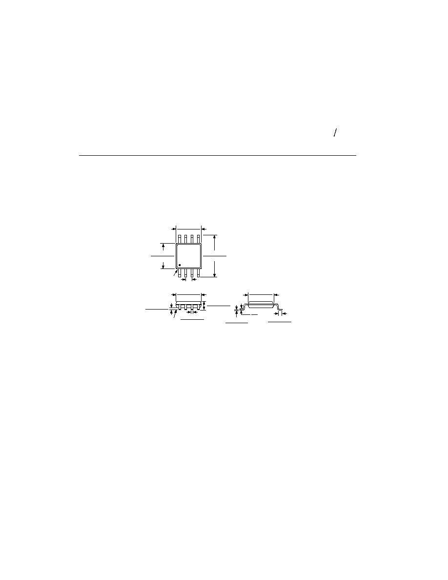
OUTLINE DIMENSIONS
Dimensions shown in inches and (mm).
8-Lead Micro SOIC (MSOP)
(RM-8)
0.011 (0.28)
0.003 (0.08)
0.028 (0.71)
0.016 (0.41)
33
27
0.120 (3.05)
0.112 (2.84)
8
5
4
1
0.122 (3.10)
0.114 (2.90)
0.199 (5.05)
0.187 (4.75)
PIN 1
0.0256 (0.65) BSC
0.122 (3.10)
0.114 (2.90)
SEATING
PLANE
0.006 (0.15)
0.002 (0.05)
0.018 (0.46)
0.008 (0.20)
0.043 (1.09)
0.037 (0.94)
0.120 (3.05)
0.112 (2.84)
CONTROLLING DIMENSIONS ARE IN MILLIMETERS. INCH DIMENSIONS
ARE ROUNDED-OFF MILLIMETER EQUIVALENTS FOR REFERENCE
ONLY AND ARE NOT APPROPRIATE FOR USE IN DESIGN.
Assuming I
LOAD
= 300 mA, I
GND
= 4 mA, V
IN
= 1.8 V and
V
OUT
= 1.2 V, device power dissipation is:
P
D
=
-
+
=
( .
. )
( . )
1 8
1 2 300
1 8 4
187
mA
mA
mW
The proprietary package used in the ADP3342 has a thermal
resistance of 110
°C/W, significantly lower than a standard
MSOP-8 package. Assuming a 4-layer board, the junction tem-
perature rise above ambient temperature will be approximately
equal to:
T
W
C W
C
A
J
=
×
°
=
°
0 187
110
20 6
.
.
Document Outline
- Specifications
- Pinout
- Package drawings
- Ordering Guide
- Features
- Applications
- Product Description
- Absolute Maximum Ratings
- Functional Block Diagram
- Pin Function Description
- Circuit Description
- CAUTION
- THEORY OF OPERATION APPLICATION INFORMATION
- DIAGRAMS
- Typical Application Circuit
- Control Loop Functional Block Diagram