 | ÐлекÑÑоннÑй компоненÑ: ADR02BR | СкаÑаÑÑ:  PDF PDF  ZIP ZIP |
Äîêóìåíòàöèÿ è îïèñàíèÿ www.docs.chipfind.ru
Ultracompact Precision
10 V/5 V/2.5 V/3.0 V Voltage References
ADR01/ADR02/ADR03/ADR06
FEATURES
Ultracompact SC70-5/TSOT-5
Low temperature coefficient
SOIC-8: 3 ppm/°C
SC70-5/TSOT-5: 9 ppm/°C
Initial accuracy ± 0.1%
No external capacitor required
Low noise 10 µV p-p (0.1 Hz to 10 Hz)
Wide operating range
ADR01: 12 V to 40 V
ADR02: 7 V to 40 V
ADR03: 4.5 V to 40 V
ADR06: 5.0 V to 40 V
High output current 10 mA
Wide temperature range: 40°C to +125°C
ADR01/ADR02/ADR03 pin compatible to industry-standard
REF01/REF02/REF03
1
APPLICATIONS
Precision data acquisition systems
High resolution converters
Industrial process control systems
Precision instruments
PCMCIA cards
SELECTION GUIDE
Part Number
Output Voltage
ADR01 10.0
V
ADR02 5.0
V
ADR03 2.5
V
ADR06 3.0
V
1
ADR01, ADR02, and ADR03 are component-level compatible with REF01,
REF02, and REF03, respectively. No guarantees for system-level compatibility
are implied. SOIC-8 versions of ADR01/ADR02/ADR03 are pin-to-pin
compatible with SOIC-8 versions of REF01/REF02/REF03, respectively, with
the additional temperature monitoring function.
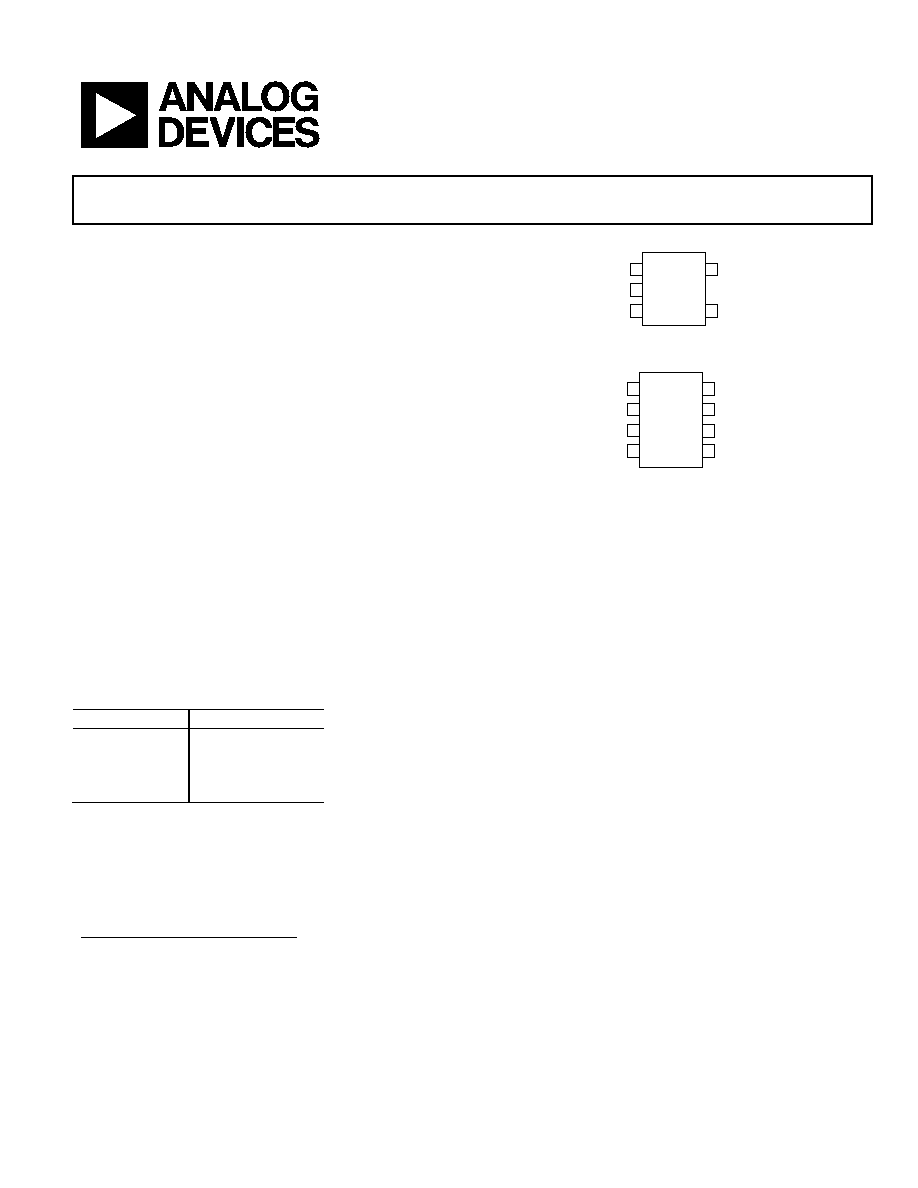
PIN CONFIGURATIONS
5
4
1
3
2
V
OUT
TRIM
V
IN
TEMP
GND
TOP VIEW
(Not to Scale)
ADR01/
ADR02/
ADR03/
ADR06
02747-F
-
001
Figure 1. 5-Lead SC70/TSOT Surface-Mount Packages
TOP VIEW
(Not to Scale)
8
6
1
TP
3
2
ADR01/
ADR02/
ADR03/
ADR06
V
OUT
7
5
4
TRIM
TP
NIC
V
IN
TEMP
GND
NIC = NO INTERNAL CONNECT
TP = TEST PIN (DO NOT CONNECT)
02747-F
-
002
Figure 2. 8-Lead SOIC Surface-Mount Package
GENERAL DESCRIPTION
The ADR01, ADR02, ADR03, and ADR06 are precision 10 V,
5 V, 2.5 V, and 3.0 V band gap voltage references featuring high
accuracy, high stability, and low power. The parts are housed in
tiny SC70-5 and TSOT-5 packages, as well as the SOIC-8
versions. The SOIC-8 versions of the ADR01, ADR02, and
ADR03 are drop-in replacements
1
to the industry-standard
REF01, REF02, and REF03. The small footprint and wide
operating range make the ADR0x references ideally suited for
general-purpose and space-constraint applications.
With an external buffer and a simple resistor network, the
TEMP terminal can be used for temperature sensing and
approximation. A TRIM terminal is provided on the devices
for fine adjustment of the output voltage.
The ADR01, ADR02, ADR03, and ADR06 are compact, low drift
voltage references that provide an extremely stable output
voltage from a wide supply voltage range. They are available in
SC70-5, TSOT-5, and SOIC-8 packages with A and B grade
selections. All parts are specified over the extended industrial
(40°C to +125°C) temperature range.
Rev. F
Information furnished by Analog Devices is believed to be accurate and reliable.
However, no responsibility is assumed by Analog Devices for its use, nor for any
infringements of patents or other rights of third parties that may result from its use.
Specifications subject to change without notice. No license is granted by implication
or otherwise under any patent or patent rights of Analog Devices. Trademarks and
registered trademarks are the property of their respective owners.
One Technology Way, P.O. Box 9106, Norwood, MA 02062-9106, U.S.A.
Tel: 781.329.4700
www.analog.com
Fax: 781.326.8703
© 2004 Analog Devices, Inc. All rights reserved.

ADR01/ADR02/ADR03/ADR06
Rev. F | Page 2 of 20
TABLE OF CONTENTS
Specifications..................................................................................... 3
ADR01 Electrical Characteristics............................................... 3
ADR02 Electrical Characteristics............................................... 4
ADR03 Electrical Characteristics............................................... 5
ADR06 Electrical Characteristics............................................... 6
Dice Electrical Characteristics.................................................... 7
Absolute Maximum Ratings............................................................ 8
Parameter Definitions ...................................................................... 9
Notes............................................................................................... 9
Typical Performance Characteristics ........................................... 10
Applications..................................................................................... 15
Applying the ADR01/ADR02/ADR03/ADR06...................... 15
Negative Reference..................................................................... 16
Low Cost Current Source.......................................................... 16
Precision Current Source with Adjustable Output ................ 16
Programmable 4 to 20 mA Current Transmitter ................... 17
Outline Dimensions ....................................................................... 18
Ordering Guides ............................................................................. 19
ADR01 Ordering Guide ............................................................ 19
ADR02 Ordering Guide ............................................................ 19
ADR03 Ordering Guide ............................................................ 20
ADR06 Ordering Guide ............................................................ 20
REVISION HISTORY
7/04--Data Sheet Changed from Rev. E to Rev. F
Changes to ADR02 Electrical Characteristics, Table 2................ 4
Changes to Ordering Guide .......................................................... 19
2/04--Data Sheet Changed from Rev. D to Rev. E
Added C grade ................................................................Universal
Changes to Outline Dimensions............................................... 19
Updated Ordering Guide........................................................... 20
8/03--Data Sheet Changed from Rev. C to Rev D
Added ADR06 Universal
Change to Figure 27 13
6/03--Data Sheet Changed from Rev. B to Rev C
Changes to Features Section 1
Changes to General Description Section 1
Changes to Figure 2 1
Changes to Specifications Section 2
Addition of Dice Electrical Characteristics and Layout 6
Changes to Absolute Maximum Ratings Section 7
Updated SOIC (R-8) Outline Dimensions 19
Changes to Ordering Guide 20
2/03--Data Sheet Changed from Rev. A to Rev. B
Added ADR03.....................................................................Universal
Added TSOT-5 (UJ) Package............................................Universal
Updated Outline Dimensions....................................................... 18
12/02--Data Sheet Changed from Rev. 0 to Rev. A
Changes to Features Section ........................................................1
Changes to General Description .................................................1
Table I deleted................................................................................1
Changes to ADR01 Specifications ..............................................2
Changes to ADR02 Specifications ..............................................3
Changes to Absolute Maximum Ratings Section .....................4
Changes to Ordering Guide.........................................................4
Updated Outline Dimensions .................................................. 12
ADR01/ADR02/ADR03/ADR06
Rev. F | Page 3 of 20
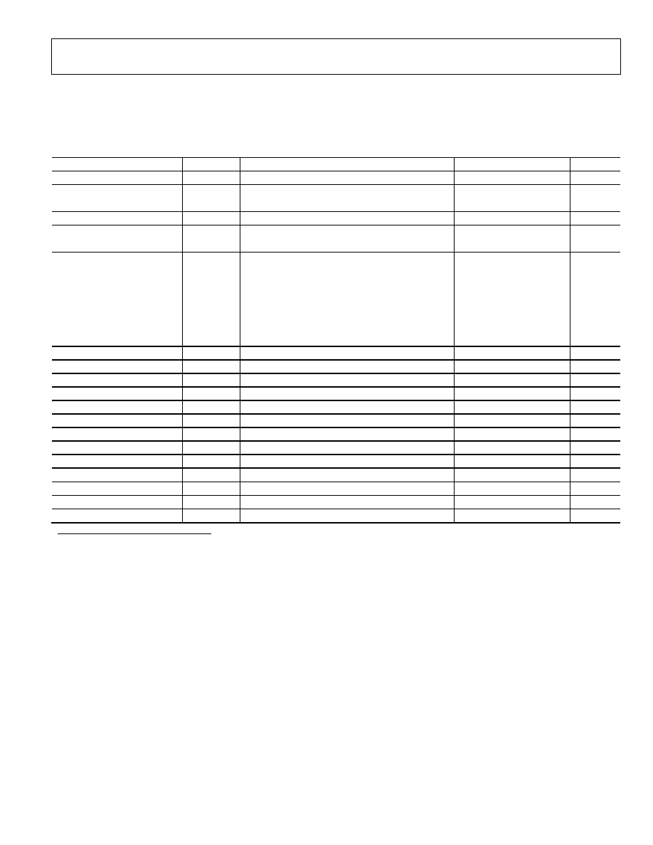
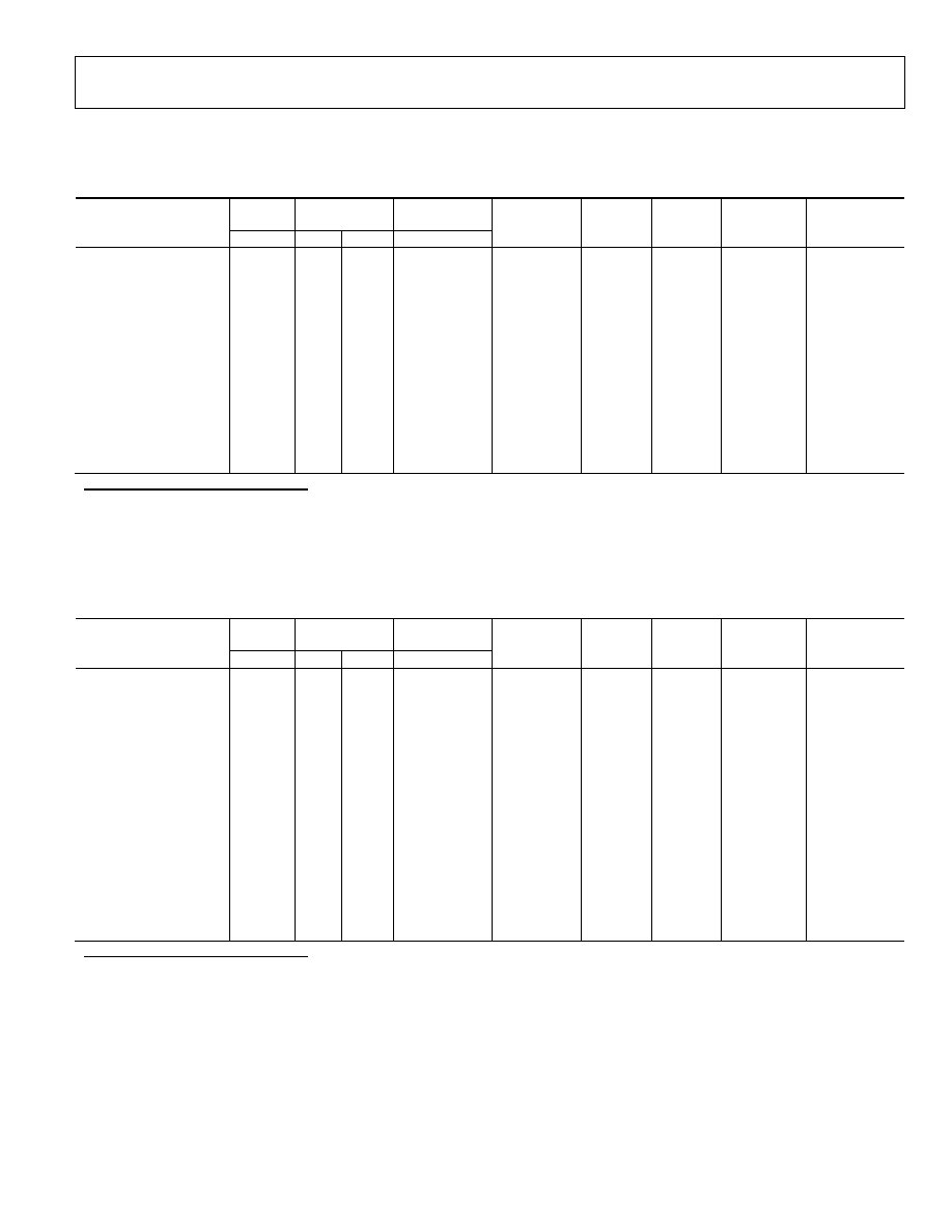
SPECIFICATIONS
ADR01 ELECTRICAL CHARACTERISTICS
V
IN
= 12 V to 40 V, T
A
= 25°C, unless otherwise noted.
Table 1.
Parameter
Symbol
Conditions
Min
Typ
Max
Unit
Output Voltage
V
O
A and C grades
9.990
10.000
10.010
V
10
mV
Initial Accuracy
V
OERR
A and C grades
0.1
%
Output Voltage
V
O
B grade
9.995
10.000
10.005
V
5 mV
Initial Accuracy
V
OERR
B grade
0.05
%
A grade, SOIC-8, 40°C < T
A
< +125°C
3
10
ppm/°C
A grade, TSOT-5, 40°C < T
A
< +125°C
25
ppm/°C
A grade, SC70-5, 40°C < T
A
< +125°C
25
ppm/°C
B grade, SOIC-8, 40°C < T
A
< +125°C
1
3
ppm/°C
B grade, TSOT-5, 40°C < T
A
< +125°C
9
ppm/°C
Temperature Coefficient
TCV
O
B grade, SC70-5, 40°C < T
A
< +125°C
9
ppm/°C
C grade, SOIC-8, 40°C < T
A
< +125°C
10
40
ppm/°C
Supply Voltage Headroom
V
IN
V
O
2
V
Line Regulation
V
O
/V
IN
V
IN
= 12 V to 40 V, 40°C < T
A
< +125°C
7
30
ppm/V
Load Regulation
V
O
/I
LOAD
I
LOAD
= 0 to 10 mA, 40°C < T
A
< +125°C, V
IN
= 15 V
40
70
ppm/mA
Quiescent Current
I
IN
No load, 40°C < T
A
< +125°C
0.65
1
mA
Voltage Noise
e
N p-p
0.1 Hz to 10 Hz
20
µV p-p
Voltage Noise Density
e
N
1 kHz
510
nV/Hz
Turn-On Settling Time
t
R
4
µs
Long-Term Stability
1
V
O
1,000 hours
50
ppm
Output Voltage Hysteresis
V
O_HYS
70
ppm
Ripple Rejection Ratio
RRR
f
IN
= 10 kHz
-75
dB
Short Circuit to GND
I
SC
30
mA
Voltage Output at TEMP Pin
V
TEMP
550
mV
Temperature Sensitivity
TCV
TEMP
1.96
mV/°C
1
The long-term stability specification is noncumulative. The drift in subsequent 1,000 hour periods is significantly lower than in the first 1,000 hour period.
ADR01/ADR02/ADR03/ADR06
Rev. F | Page 4 of 20
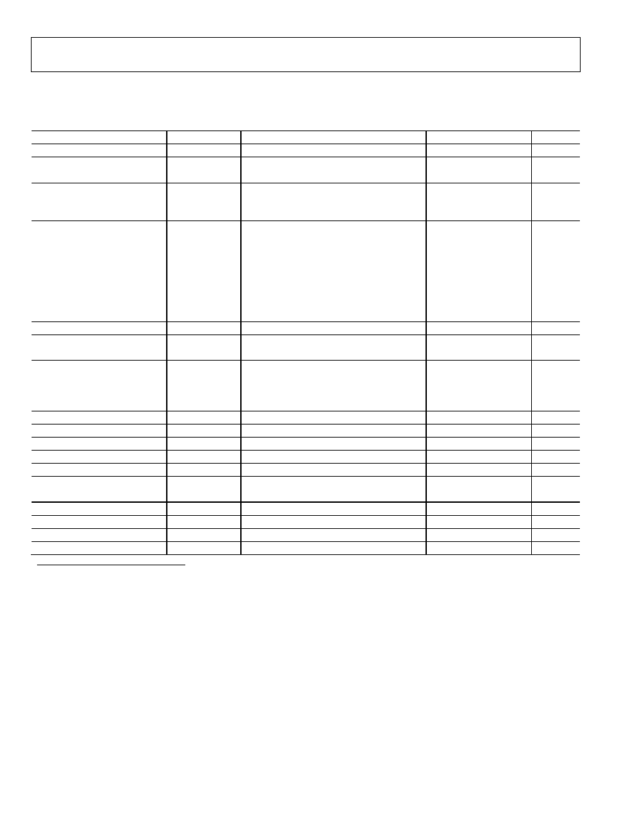
ADR02 ELECTRICAL CHARACTERISTICS
V
IN
= 7 V to 40 V, T
A
= 25°C, unless otherwise noted.
Table 2.
Parameter
Symbol
Conditions
Min
Typ
Max
Unit
Output Voltage
V
O
A and C grades
4.995
5.000
5.005
V
5
mV
Initial Accuracy
V
OERR
A and C grades
0.1
%
Output Voltage
V
O
B grade
4.997
5.000
5.003
V
3
mV
Initial Accuracy
V
OERR
B grade
0.06
%
A grade, SOIC-8, 40°C < T
A
< +125°C
3
10
ppm/°C
A grade, TSOT-5, 40°C < T
A
< +125°C
25
ppm/°C
A grade, SC70-5, 40°C < T
A
< +125°C
A grade. SC70-5, -55
o
C < TA < +125
o
C
25
30
ppm/°C
ppm/°C
B grade, SOIC-8, 40°C < T
A
< +125°C
1
3
ppm/°C
B grade, TSOT-5, 40°C < T
A
< +125°C
9
ppm/°C
Temperature Coefficient
TCV
O
B grade, SC70-5, 40°C < T
A
< +125°C
9
ppm/°C
C grade, SOIC-8, 40°C < T
A
< +125°C
10
40
ppm/°C
Supply Voltage Headroom
V
IN
V
O
2
V
Line Regulation
V
O
/V
IN
V
IN
= 7 V to 40 V, 40°C < T
A
< +125°C
V
IN
= 7 V to 40 V, 55°C < T
A
< +125°C
7
7
30
40
ppm/V
ppm/V
Load Regulation
V
O
/I
LOAD
I
LOAD
= 0 to 10 mA, 40°C < T
A
< +125°C,
V
IN
= 10 V
I
LOAD
= 0 to 10 mA, 55°C < T
A
< +125°C,
V
IN
= 10 V
40
45
70
80
ppm/mA
ppm/mA
Quiescent Current
I
IN
No load, 40°C < T
A
< +125°C
0.65
1
mA
Voltage Noise
e
N p-p
0.1 Hz to 10 Hz
10
µV p-p
Voltage Noise Density
e
N
1 kHz
230
nV/Hz
Turn-On Settling Time
t
R
4
µs
Long-Term Stability
1
V
O
1,000 hours
50
ppm
Output Voltage Hysteresis
V
O_HYS
55°C < T
A
< +125°C
70
80
ppm
ppm
Ripple Rejection Ratio
RRR
f
IN
= 10 kHz
75
dB
Short Circuit to GND
I
SC
30
mA
Voltage Output at TEMP Pin
V
TEMP
550
mV
Temperature Sensitivity
TCV
TEMP
1.96
mV/°C
1
The long-term stability specification is noncumulative. The drift in subsequent 1,000 hour periods is significantly lower than in the first 1,000 hour period.
ADR01/ADR02/ADR03/ADR06
Rev. F | Page 5 of 20
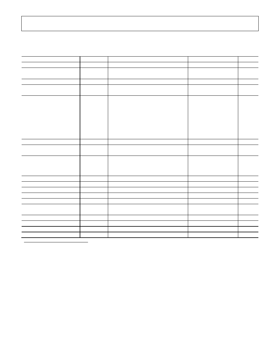
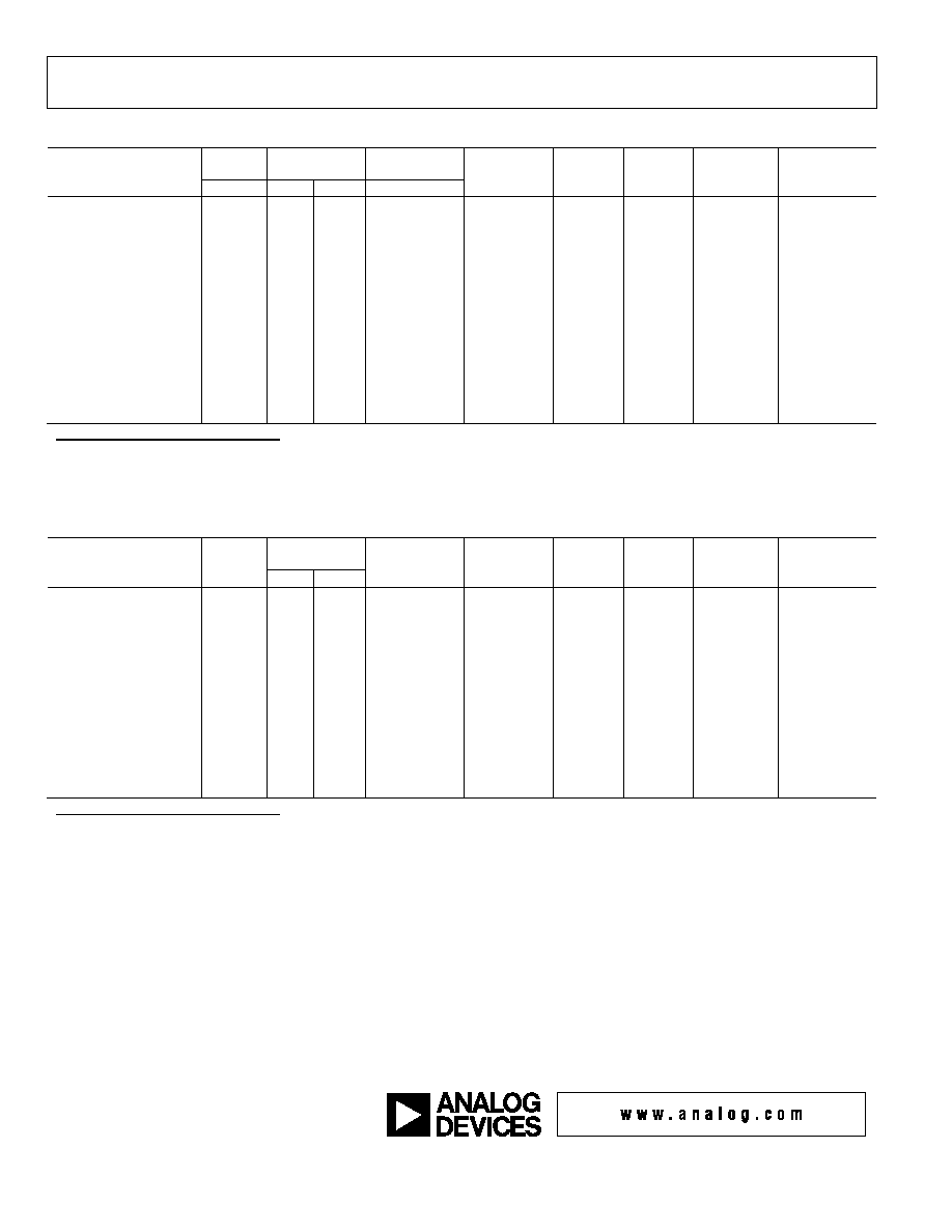
ADR03 ELECTRICAL CHARACTERISTICS
V
IN
= 4.5 V to 40 V, T
A
= 25°C, unless otherwise noted.
Table 3.
Parameter
Symbol
Conditions
Min
Typ
Max
Unit
Output Voltage
V
O
A and C grades
2.495
2.500
2.505
V
5
mV
Initial Accuracy
V
OERR
A and C grades
0.2
%
Output Voltage
V
O
B
grades
2.4975 2.5000 2.5025 V
2.5
mV
Initial Accuracy
V
OERR
B grades
0.1
%
A grade, SOIC-8, 40°C < T
A
< +125°C
3
10
ppm/°C
A grade, TSOT-5, 40°C < T
A
< +125°C
25
ppm/°C
A grade, SC70-5, 40°C < T
A
< +125°C
A grade, SC70-5, 55°C < T
A
< +125°C
25
30
ppm/°C
ppm/°C
B grade, SOIC-8, 40°C < T
A
< +125°C
1
3
ppm/°C
B grade, TSOT-5, 40°C < T
A
< +125°C
9
ppm/°C
Temperature Coefficient
TCV
O
B grade, SC70-5, 40°C < T
A
< +125°C
9
ppm/°C
C grade, SOIC-8, 40°C < T
A
< +125°C
10
40
ppm/°C
Supply Voltage Headroom
V
IN
V
O
2 V
Line Regulation
V
O
/V
IN
V
IN
= 7.5 V to 40 V, 40°C < T
A
< +125°C
V
IN
= 7.5 V to 40 V, 55°C < T
A
< +125°C
7
7
30
40
ppm/V
ppm/V
Load Regulation
V
O
/I
LOAD
I
LOAD
= 0 mA to 10 mA, 40°C < T
A
< +125°C,
V
IN
= 7.0 V
I
LOAD
= 0 mA to 10 mA, 55°C < T
A
< +125°C,
V
IN
= 7.0 V
25
45
70
80
ppm/mA
ppm/mA
Quiescent Current
I
IN
No load, 40°C < T
A
< +125°C
0.65
1
mA
Voltage Noise
e
N p-p
0.1 Hz to 10 Hz
6
µV p-p
Voltage Noise Density
e
N
1 kHz
230
nV/Hz
Turn-On Settling Time
t
R
4
µs
Long-Term Stability
1
V
O
1,000 hours
50
ppm
Output Voltage Hysteresis
V
O_HYS
55°C < T
A
< +125°C
70
80
ppm
ppm
Ripple Rejection Ratio
RRR
f
IN
= 10 kHz
75
dB
Short Circuit to GND
I
SC
30
mA
Voltage Output at TEMP Pin
V
TEMP
550
mV
Temperature Sensitivity
TCV
TEMP
1.96
mV/°C
1
The long-term stability specification is noncumulative. The drift in subsequent 1,000 hour periods is significantly lower than in the first 1,000 hour period.
ADR01/ADR02/ADR03/ADR06
Rev. F | Page 6 of 20
ADR06 ELECTRICAL CHARACTERISTICS
V
IN
= 5.0 V to 40 V, T
A
= 25°C, unless otherwise noted.
Table 4.
Parameter
Symbol
Conditions
Min
Typ
Max
Unit
Output Voltage
V
O
A and C grades
2.994
3.000
3.006
V
6
mV
Initial Accuracy
V
OERR
A and C grades
0.2
%
Output Voltage
V
O
B
grade
2.997 3.000 3.003 V
3
mV
Initial Accuracy
V
OERR
B grade
0.1
%
A grade, SOIC-8, 40°C < T
A
< +125°C
3
10
ppm/°C
A grade, TSOT-5, 40°C < T
A
< +125°C
25
ppm/°C
A grade, SC70-5, 40°C < T
A
< +125°C
25
ppm/°C
B grade, SOIC-8, 40°C < T
A
< +125°C
1
3
ppm/°C
B grade, TSOT-5, 40°C < T
A
< +125°C
9
ppm/°C
Temperature Coefficient
TCV
O
B grade, SC70-5, 40°C < T
A
< +125°C
9
ppm/°C
C grade, SOIC-8, 40°C < T
A
< +125°C
10
40
ppm/°C
Supply Voltage Headroom
V
IN
V
O
2 V
Line Regulation
V
O
/V
IN
V
IN
= 15 V to 40 V, 40°C < T
A
< +125°C
7
30
ppm/V
Load Regulation
V
O
/I
LOAD
I
LOAD
= 0 to 10 mA, 40°C < T
A
< +125°C, V
IN
=
7.0 V
40 70 ppm/mA
Quiescent Current
I
IN
No load, 40°C < T
A
< +125°C
0.65
1
mA
Voltage Noise
e
N p-p
0.1 Hz to 10 Hz
10
µV p-p
Voltage Noise Density
e
N
1 kHz
510
nV/Hz
Turn-On Settling Time
t
R
4
µs
Long-Term Stability
1
V
O
1,000 hours
50
ppm
Output Voltage Hysteresis
V
O_HYS
70
ppm
Ripple Rejection Ratio
RRR
f
IN
= 10 kHz
75
dB
Short Circuit to GND
I
SC
30
mA
Voltage Output AT TEMP Pin
V
TEMP
550
mV
Temperature Sensitivity
TCV
TEMP
1.96
mV/°C
1
The long-term stability specification is noncumulative. The drift in subsequent 1,000 hour periods is significantly lower than in the first 1,000 hour period.
ADR01/ADR02/ADR03/ADR06
Rev. F | Page 7 of 20
DICE ELECTRICAL CHARACTERISTICS
V
IN
= up to 40 V, T
A
= 25°C, unless otherwise noted.
Table 5.
Parameter
Symbol
Conditions
Min
Typ
Max
Unit
Output
Voltage
ADR01NBC
V
O
25°C
9.995 10.004 10.005 V
ADR02NBC
V
O
25°C
4.997
5.002 5.003 V
Temperature Coefficient
TCV
O
40°C < T
A
< +125°C
10
ppm/°C
Line
Regulation
ADR01NBC
V
O
/V
IN
V
IN
= 15 V to 40 V
7
ppm/V
ADR02NBC
V
O
/V
IN
V
IN
= 7 V to 40 V
7
ppm/V
Load Regulation
V
O
/I
LOAD
I
LOAD
= 0 to 10 mA
40
ppm/mA
Quiescent Current
I
IN
No load
0.65
mA
Voltage Noise
e
N p-p
0.1 Hz to 10 Hz
25
µV p-p
TEMP
GND
TRIM
V
OUT
(SENSE)
V
OUT
(FORCE)
V
IN
02747-F
-
003
DIE SIZE: 0.83mm × 1.01mm
Figure 3. Die Layout
ADR01/ADR02/ADR03/ADR06
Rev. F | Page 8 of 20
ABSOLUTE MAXIMUM RATINGS
Ratings at 25°C, unless otherwise noted.
Table 6.
Parameter Rating
Supply Voltage
40 V
Output Short-Circuit Duration to GND
Indefinite
Storage Temperature Range
65°C to +150°C
Operating Temperature Range
40°C to +125°C
Junction Temperature Range: KS, UJ, and
R Packages
65°C to +150°C
Lead Temperature Range (Soldering, 60 Sec)
300°C
Stresses above those listed under Absolute Maximum Ratings
may cause permanent damage to the device. This is a stress
rating only; functional operation of the device at these or any
other conditions above those listed in the operational sections
of this specification is not implied. Exposure to absolute
maximum rating conditions for extended periods may affect
device reliability.
Table 7. Thermal Resistance
Package Type
JA
1
JC
Unit
SC70-5 (KS-5)
376
189
°C/W
TSOT-5 (UJ-5)
230
146
°C/W
SOIC-8 (R-8)
130
43
°C/W
1
JA
is specified for the worst-case conditions, that is,
JA
is specified for
devices soldered in circuit boards for surface-mount packages.
ESD CAUTION
ESD (electrostatic discharge) sensitive device. Electrostatic charges as high as 4000 V readily accumulate on
the human body and test equipment and can discharge without detection. Although these products feature
proprietary ESD protection circuitry, permanent damage may occur on devices subjected to high energy
electrostatic discharges. Therefore, proper ESD precautions are recommended to avoid performance
degradation or loss of functionality.

ADR01/ADR02/ADR03/ADR06
Rev. F | Page 9 of 20
PARAMETER DEFINITIONS
Temperature Coefficient
The change of output voltage with respect to operating tem-
perature changes normalized by the output voltage at 25°C. This
parameter is expressed in ppm/°C and can be determined by the
following equation:
6
10
)
25
(
)
(
)
(
]
/
[
×
-
×
°
-
=
°
1
2
O
1
O
2
O
O
T
T
C
V
T
V
T
V
C
ppm
TCV
where:
V
O
(25°C) = V
O
at 25°C
V
O
(T
1
) = V
O
at Temperature 1
V
O
(T
2
) = V
O
at Temperature 2
Line Regulation
The change in output voltage due to a specified change in input
voltage. This parameter accounts for the effects of self-heating.
Line regulation is expressed in either percent per volt, parts-
per-million per volt, or microvolts per volt change in input
voltage.
Load Regulation
The change in output voltage due to a specified change in load
current. This parameter accounts for the effects of self-heating.
Load regulation is expressed in either microvolts per milliampere,
parts-per-million per milliampere, or ohms of dc output
resistance.
Long-Term Stability
Typical shift of output voltage at 25°C on a sample of parts
subjected to a test of 1,000 hours at 25°C:
)
(
)
(
1
O
0
O
O
t
V
t
V
V
-
=
6
10
)
(
)
(
)
(
]
[
×
-
=
0
O
1
O
0
O
O
t
V
t
V
t
V
ppm
V
where:
V
O
(t
0
) = V
O
at 25°C at Time 0
V
O
(t
1
) = V
O
at 25°C after 100 hours of operation at 25°C
The majority of the shift is seen in the first 200 hours, and,
as time goes by, the drift decreases significantly. So for the
subsequent 1,000 hours' time points, this drift is much smaller
than the first.
Thermal Hysteresis
Defined as the change of output voltage after the device is
cycled through temperature from +25°C to 40°C to +125°C
and back to +25°C. This is a typical value from a sample of parts
put through such a cycle.
TC
O
O
HYS
O
V
C
V
V
_
_
)
25
(
-
°
=
6
_
_
10
)
25
(
)
25
(
]
[
×
°
-
°
=
C
V
V
C
V
ppm
V
O
TC
O
O
HYS
O
where:
V
O
(25°C) = V
O
at 25°C
V
O_TC
= V
O
at 25°C after temperature cycle at +25°C to 40°C to
+125°C and back to +25°C
NOTES
Input Capacitor
Input capacitors are not required on the ADR01/ADR02/
ADR03/ADR06. There is no limit for the value of the capacitor
used on the input, but a 1 µF to 10 µF capacitor on the input
improves transient response in applications where the supply
suddenly changes. An additional 0.1 µF in parallel also helps to
reduce noise from the supply.
Output Capacitor
The ADR01/ADR02/ADR03/ADR06 do not require output
capacitors for stability under any load condition. An output
capacitor, typically 0.1 µF, filters out any low level noise voltage
and does not affect the operation of the part. On the other hand,
the load transient response can be improved with an additional
1 µF to 10 µF output capacitor in parallel. A capacitor here acts
as a source of stored energy for a sudden increase in load
current. The only parameter that degrades by adding an output
capacitor is the turn-on time, and it depends on the size of the
capacitor chosen.
ADR01/ADR02/ADR03/ADR06
Rev. F | Page 10 of 20
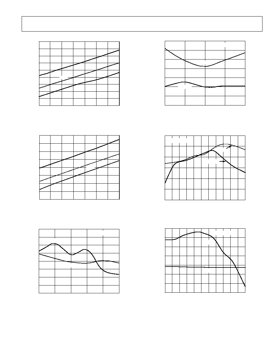
TYPICAL PERFORMANCE CHARACTERISTICS
TEMPERATURE (
o
C)
V
OU
T
(V
)
10.010
10.005
10.000
9.995
9.990
9.985
40 25 10
5
20
35
50
65
80
95
110
125
02747-F
-
004
Figure 4. ADR01 Typical Output Voltage vs. Temperature
TEMPERATURE (
o
C)
V
OU
T
(V)
5.008
5.004
5.000
4.996
4.992
40 25 10
5
20
35
50
65
80
95
110
125
02747-F
-
005
Figure 5. ADR02 Typical Output Voltage vs. Temperature
TEMPERATURE (
o
C)
40
V
OU
T
(V
)
2.502
2.501
25 10
5
20
35
50
65
80
95
110
125
2.500
2.499
2.498
02747-F
-
006
Figure 6. ADR03 Typical Output Voltage vs. Temperature
TEMPERATURE (
o
C)
V
OU
T
(V
)
3.002
3.001
3.000
2.999
2.998
40 25 10
5
20
35
50
65
80
95
110
125
02747-F
-
007
Figure 7. ADR06 Typical Output Voltage vs. Temperature
12
28
16
20
24
32
36
40
S
U
P
P
L
Y
CURRE
NT
(m
A)
0.8
0.7
0.6
0.5
0.4
INPUT VOLTAGE (V)
+125
o
C
+25
o
C
40
o
C
02747-F
-
008
Figure 8. ADR01 Supply Current vs. Input Voltage
12
28
16
20
24
32
36
40
8
INP
U
T CURRE
NT
(m
A)
+125
o
C
0.8
0.7
0.6
0.5
0.4
INPUT VOLTAGE (V)
+25
o
C
40
o
C
02747-F
-
009
Figure 9. ADR02 Supply Current vs. Input Voltage
ADR01/ADR02/ADR03/ADR06
Rev. F | Page 11 of 20
INPUT VOLTAGE (V)
5
S
U
P
P
L
Y
CURRE
NT
(m
A)
10
15
20
25
30
35
40
0.40
0.45
0.50
0.55
0.60
0.65
0.70
0.75
0.80
0.85
+125
o
C
40
o
C
+25
o
C
02747-F
-
010
Figure 10. ADR03 Supply Current vs. Input Voltage
INPUT VOLTAGE (V)
5
SUPPLY CURRENT
(
m
A)
10
15
20
25
30
35
40
0.40
0.45
0.50
0.55
0.60
0.65
0.70
0.75
0.80
+125
o
C
40
o
C
+25
o
C
02747-F
-
011
Figure 11. ADR06 Supply Current vs. Input Voltage
40
25
20
0
85
125
30
10
I
L
= 0mA TO 10mA
LO
AD
REG
U
LATIO
N
(
ppm
/m
A)
TEMPERATURE (
o
C)
V
IN
= 40V
V
IN
= 14V
50
0
40
40
30
20
10
02747-F
-
012
Figure 12. ADR01 Load Regulation vs. Temperature
40
20
0
50
85
125
30
10
I
L
= 0mA TO 5mA
LO
AD RE
G
U
LATIO
N
(ppm
/m
A)
TEMPERATURE (
o
C)
V
IN
= 40V
V
IN
= 8V
25
0
40
20
10
02747-F
-
013
Figure 13. ADR02 Load Regulation vs. Temperature
LO
AD RE
G
U
LATIO
N
(ppm
/m
A)
0
10
20
30
40
50
60
TEMPERATURE (
o
C)
40 25 10
5
20
35
50
65
80
95
110
125
V
IN
= 40V
V
IN
= 7V
I
L
= 0mA TO 10mA
02747-F
-
014
Figure 14. ADR03 Load Regulation vs. Temperature
LO
AD REG
U
LATIO
N
(ppm
/m
A)
30
20
10
0
10
20
40
30
TEMPERATURE (
o
C)
40 25 10
5
20
35
50
65
80
95
110
125
V
IN
= 40V
I
L
= 0mA TO 10mA
V
IN
= 7V
02747-F
-
015
Figure 15. ADR06 Load Regulation vs. Temperature
ADR01/ADR02/ADR03/ADR06
Rev. F | Page 12 of 20
0
4
2
2
6
8
TEMPERATURE (
o
C)
LINE
RE
G
U
LATIO
N
(ppm
/V
)
10
40 25 10
5
20
35
50
65
80
95
110 125
V
IN
= 14V TO 40V
02747-F
-
016
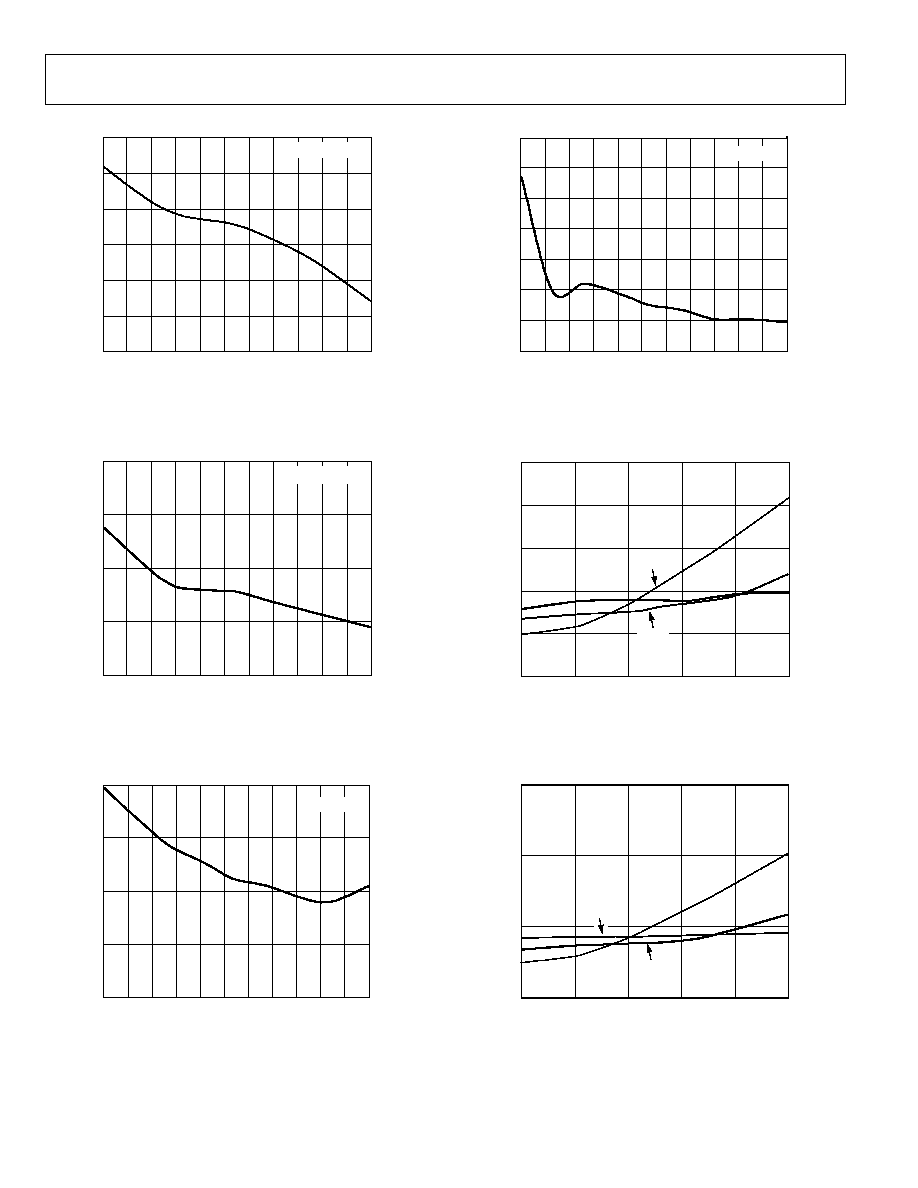
Figure 16. ADR01 Line Regulation vs. Temperature
4
4
8
0
8
TEMPERATURE (
o
C)
LINE
RE
G
U
LATIO
N
(
ppm
/V
)
V
IN
= 8V TO 40V
40 25 10
5
20
35
50
65
80
95
110
125
02747-F
-
017
Figure 17. ADR02 Line Regulation vs. Temperature
LINE REGULATION
(ppm/mV)
4
2
0
2
4
TEMPERATURE (
o
C)
40
25 10
5
20
35
50
65
80
95
110
125
02747-
F
-
018
V
IN
= 5V TO 40V
Figure 18. ADR03 Line Regulation vs. Temperature
LINE REG
U
LATIO
N
(ppm
/V)
4
2
2
4
6
0
8
10
TEMPERATURE (
o
C)
40
25 10
5
20
35
50
65
80
95
110
125
02747-F-019
V
IN
= 6V TO 40V
Figure 19. ADR06 Line Regulation vs. Temperature
3
1
5
2
0
4
4
6
0
2
LOAD CURRENT (mA)
8
10
DIFFE
RE
NTIAL
V
O
LTAG
E
(
V
)
40
o
C
+125
o
C
+25
o
C
02747-F
-
020
Figure 20. ADR01 Minimum Input-Output
Voltage Differential vs. Load Current
4
6
8
0
2
0
4
2
+25
o
C
LOAD CURRENT (mA)
8
10
40
o
C
+125
o
C
DIFFERENTIAL VO
LTAG
E
(
V
)
02747-F
-
021
Figure 21. ADR02 Minimum Input-Output
Voltage Differential vs. Load Current
ADR01/ADR02/ADR03/ADR06
Rev. F | Page 13 of 20
3
1
5
2
0
4
4
6
0
2
LOAD CURRENT (mA)
8
10
DIFFERENTIAL
V
O
LTAG
E
(
V
)
+125
o
C
+25
o
C
40
o
C
6
02747-F
-
022
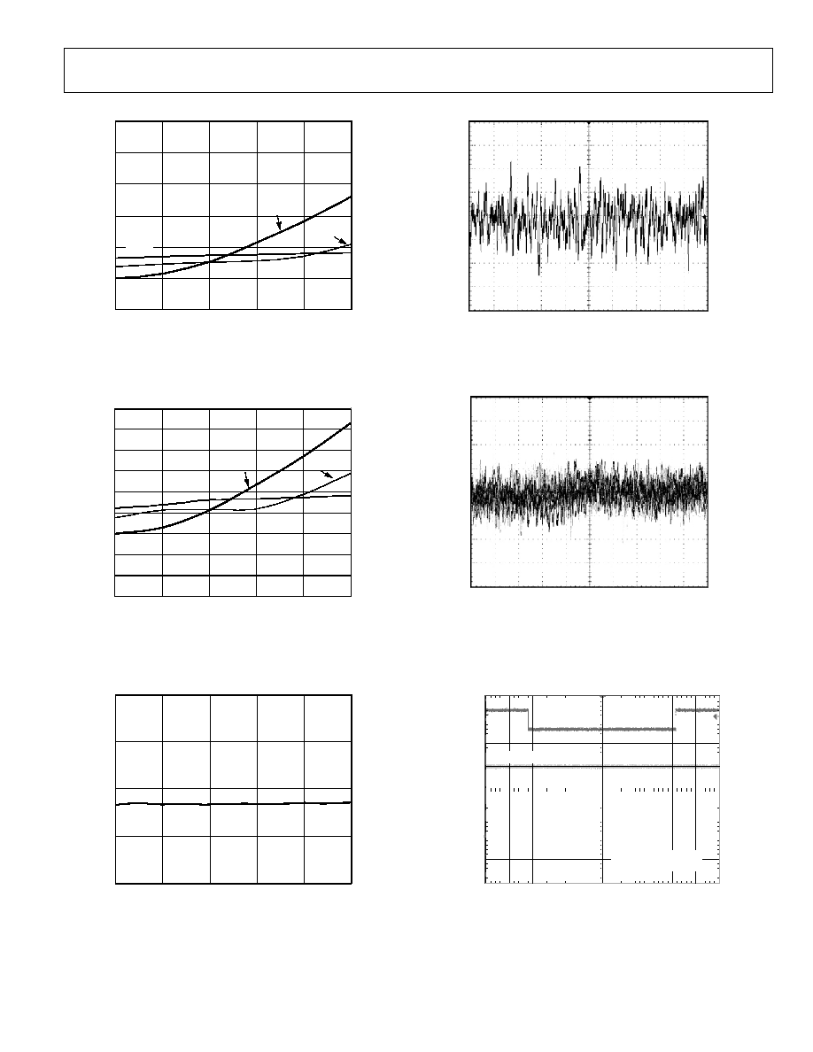
Figure 22. ADR03 Minimum Input-Output
Voltage Differential vs. Load Current
2.0
1.0
4.0
3.5
3.0
1.5
0
0.5
2.5
0
2
4
6
LOAD CURRENT (mA)
8
10
DIFFERENTIAL
V
OLTAGE (
V
)
+125
o
C
+25
o
C
40
o
C
4.5
02747-
F
-
023
Figure 23. ADR06 Minimum Input-Output
Voltage Differential vs. Load Current
4
6
0
0.50
2
T
A
= 25
o
C
LOAD CURRENT (mA)
8
10
Q
U
IESCENT CURRENT (m
A)
0.55
0.60
0.65
0.70
02747-
F
-
024
Figure 24. ADR01 Quiescent Current vs. Load Current
1
µ
V/D
I
V
TIME (1s/DIV)
02747-F
-
025
Figure 25. ADR02 Typical Noise Voltage 0.1 Hz to 10 Hz
50
µ
V/D
I
V
TIME (1ms/DIV)
02747-F
-
026
Figure 26. ADR02 Typical Noise Voltage 10 Hz to 10 KHz
NO LOAD CAPACITOR
NO INPUT CAPACITOR
V
OUT
5V/DIV
TIME (2.00ms/DIV)
02747-F
-
027
10V
8V
Figure 27. ADR02 Line Transient Response
ADR01/ADR02/ADR03/ADR06
Rev. F | Page 14 of 20
V
IN
5V/DIV
V
OUT
100mV/DIV
TIME (1.00ms/DIV)
NO LOAD CAPACITOR
LOAD OFF
LOAD ON
LOAD = 5mA
02747-
F
-
028
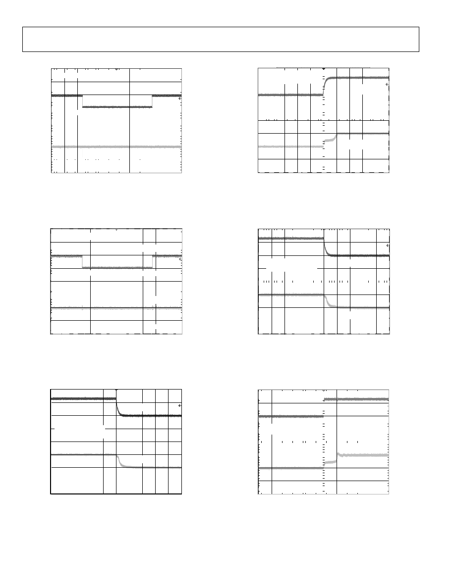
Figure 28. ADR02 Load Transient Response
C
LOAD
= 100nF
V
IN
5V/DIV
V
OUT
100mV/DIV
TIME (1.00ms/DIV)
02747-F
-
029
LOAD OFF
LOAD ON
LOAD = 5mA
Figure 29. ADR02 Load Transient Response
C
IN
= 0.01
µ
F
NO LOAD CAPACITOR
V
IN
10V/DIV
V
OUT
5V/DIV
TIME (4
µ
s/DIV)
02747-
F
-
030
Figure 30. ADR02 Turn-Off Response
V
IN
10V/DIV
V
OUT
5V/DIV
TIME (4
µ
s/DIV)
C
IN
= 0.01
µ
F
NO LOAD CAPACITOR
02747-
F
-
031
Figure 31. ADR02 Turn-On Response
V
IN
10V/DIV
V
OUT
5V/DIV
TIME (4
µ
s/DIV)
C
L
= 0.01
µ
F
NO INPUT CAPACITOR
02747-
F
-
032
Figure 32. ADR02 Turn-Off Response
V
OUT
5V/DIV
V
IN
10V/DIV
TIME (4
µ
s/DIV)
C
L
= 0.01
µ
F
NO INPUT CAPACITOR
02747-
F
-
033
Figure 33. ADR02 Turn-On Response
ADR01/ADR02/ADR03/ADR06
Rev. F | Page 15 of 20
APPLICATIONS
The ADR01/ADR02/ADR03/ADR06 are high precision, low
drift 10 V, 5 V, 2.5 V, and 3.0 V voltage references available in an
ultracompact footprint. The SOIC-8 version of the devices is a
drop-in replacement of the REF01/REF02/ REF03 sockets with
improved cost and performance.
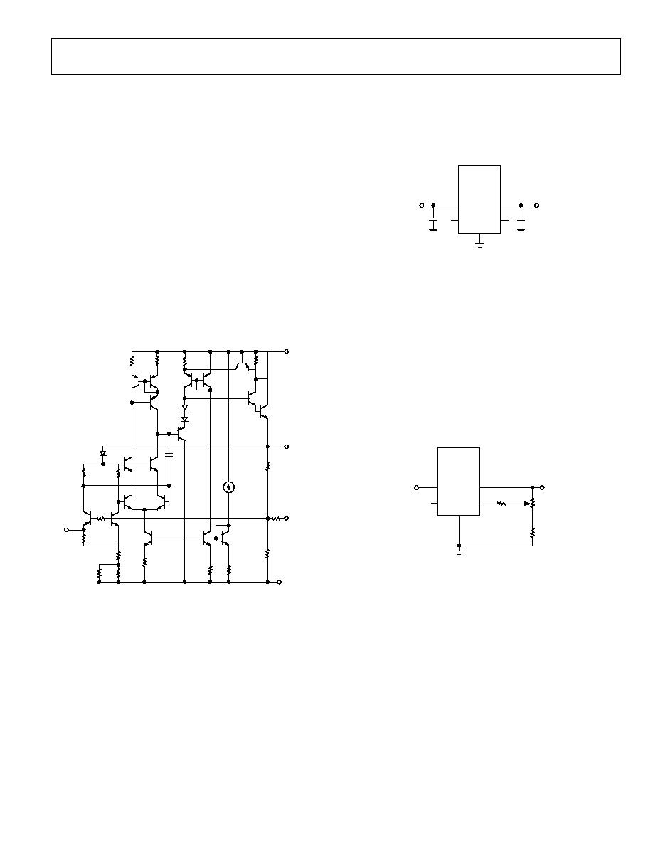
These devices are standard band gap references. The band gap
cell contains two NPN transistors (Q18 and Q19) that differ in
emitter area by 2×. The difference in their V
BE
produces a
proportional-to-absolute temperature current (PTAT) in R14,
and, when combined with the V
BE
of Q19, produces a band gap
voltage, V
BG,
that is almost constant in temperature. With an
internal op amp and the feedback network of R5
and R6, V
O
is set
precisely at 10 V, 5 V, 2.5 V, and 3.0 V for the ADR01, ADR02,
ADR06, and ADR03, respectively. Precision laser trimming of
the resistors and other proprietary circuit techniques are used to
further enhance the initial accuracy, temperature curvature, and
drift performance of the ADR01/ADR02/ADR03/ADR06.
R1
R2
R3
R4
V
IN
Q23
Q1
Q2
Q7
Q8
Q9
Q3
Q10
D1
D2
Q4
V
O
D3
C1
R13
Q12
Q13
R5
I1
R12
Q14Q15
2X
1X
V
BG
R20
TRIM
Q18
TEMP
R27
Q19
Q16
Q17
Q20
R6
R42
R41
R24
R32
R11
R17
R14
GND
02747-F
-
034
Figure 34. Simplified Schematic Diagram
The PTAT voltage is made available at the TEMP pin of the
ADR01/ADR02/ADR03/ADR06. It has a stable 1.96 mV/°C
temperature coefficient, such that users can estimate the
temperature change of the device by knowing the voltage
change at the TEMP pin.
APPLYING THE ADR01/ADR02/ADR03/ADR06
The devices can be used without any external components to
achieve the specified performance. Because of the internal op
amp amplifying the band gap cell to 10 V/5 V/2.5 V/3.0 V,
power supply decoupling helps the transient response of the
ADR01/ADR02/ADR03/ADR06. As a result, a 0.1 µF ceramic
type decoupling capacitor should be applied as close as possible
to the input and output pins of the device. An optional 1 µF to
10 µF bypass capacitor can also be applied at the V
IN
node to
maintain the input under transient disturbance.
U1
ADR01/
ADR02/
ADR03/
ADR06
V
O
C2
0.1
µ
F
C1
0.1
µ
F
V
IN
V
IN
V
OUT
TEMP TRIM
GND
02747-F
-035
Figure 35. Basic Configuration
Output Adjustment
The ADR01/ADR02/ADR03/ADR06 trim terminal can be used
to adjust the output voltage over a nominal voltage. This feature
allows a system designer to trim system errors by setting the
reference to a voltage other than 10 V/5 V/2.5 V/3.0 V. For finer
adjustment, a series resistor of 470 k can be added. With the
configuration shown in Figure 36, the ADR01 can be adjusted
from 9.70 V to 10.05 V, the ADR02 can be adjusted from 4.95 V
to 5.02 V, the ADR06 can be adjusted from 2.8 V to 3.3 V, and
the ADR03 can be adjusted from 2.3 V to 2.8 V. Adjustment of
the output does not significantly affect the temperature per-
formance of the device, provided the temperature coefficients of
the resistors are relatively low.
U1
ADR01/
ADR02/
ADR03/
ADR06
V
IN
V
OUT
TEMP TRIM
GND
V
IN
V
O
pot
10k
R2
1k
R1
470k
02747-F
-
036
Figure 36. Optional Trim Adjustment
Temperature Monitoring
As described previously, the ADR01/ADR02/ADR03/ADR06
provide a TEMP output (Pin 3) that varies linearly with tem-
perature. This output can be used to monitor the temperature
change in the system. The voltage at VTEMP is approximately
550 mV at 25°C, and the temperature coefficient is approximately
1.96 mV/°C (see Figure 37). A voltage change of 39.2 mV at the
TEMP pin corresponds to a 20°C change in temperature.
ADR01/ADR02/ADR03/ADR06
Rev. F | Page 16 of 20
02747-
F
-
037
125
25
50
75
100
0.40
0.80
0.75
0.70
0.65
0.60
0.55
0.50
0.45
25
0
50
V
IN
= 15V
SAMPLE SIZE = 5
V
TEMP
(V
)
TEMPERATURE (
o
C)
V
TEMP
/
T 1.96mV/
o
C
Figure 37. Voltage at TEMP Pin vs. Temperature
The TEMP function is provided as a convenience rather than a
precise feature. Because the voltage at the TEMP node is
acquired from the band gap core, current pulling from this pin
has a significant effect on V
OUT
. Care must be taken to buffer the
TEMP output with a suitable low bias current op amp, such as
the AD8601, AD820, or OP1177, all of which would result in
less than a 100 µV change in V
OUT
(see Figure 38). Without
buffering, even tens of microamps drawn from the TEMP pin
can cause V
OUT
to fall out of specification.
U2
15V
U1
ADR01/
ADR02/
ADR03/
ADR06
V
IN
V
OUT
TEMP TRIM
GND
V
O
V
V+
OP1177
V
TEMP
1.9mV/
o
C
V
IN
02747-
F
-
038
Figure 38. Temperature Monitoring
NEGATIVE REFERENCE
Without using any matching resistors, a negative reference can
be configured as shown in Figure 39. For the ADR01, the volt-
age difference between V
OUT
and GND is 10 V. Because V
OUT
is
at virtual ground, U2 closes the loop by forcing the GND pin to
be the negative reference node. U2 should be a precision op
amp with a low offset voltage characteristic.
U2
+15V
15V
V
V+
OP1177
V
REF
U1
ADR01/
ADR02/
ADR03/
ADR06
V
IN
V
OUT
TEMP TRIM
GND
5V TO 15V
02747-F
-
039
Figure 39. Negative Reference
LOW COST CURRENT SOURCE
Unlike most references, the ADR01/ADR02/ADR03/ADR06
employ an NPN Darlington in which the quiescent current
remains constant with respect to the load current, as shown in
Figure 24. As a result, a current source can be configured as
shown in Figure 40 where I
SET
= (V
OUT
V
L
)/R
SET
. I
L
is simply
the sum of I
SET
and I
Q
. Although simple, I
Q
varies typically from
0.55 to 0.65 mA, limiting this circuit to general-purpose
applications.
ADR01/
ADR02/
ADR03/
ADR06
V
OUT
GND
V
IN
I
IN
I
SET
= 10V/R
SET
R
SET
I
Q
0.6mA
I
L
= I
SET
+ I
Q
V
L
R
L
02747-F
-
040
Figure 40. Low Cost Current Source
PRECISION CURRENT SOURCE WITH
ADJUSTABLE OUTPUT
A precision current source, on the other hand, can be
implemented with the circuit shown in Figure 41. By adding a
mechanical or digital potentiometer, this circuit becomes an
adjustable current source. If a digital potentiometer is used, the
load current is simply the voltage across terminals B to W of the
digital potentiometer divided by R
SET
.
SET
REF
L
R
D
V
I
×
=
(1)
where D is the decimal equivalent of the digital potentiometer
input code.
U2
+12V
12V
W
B
A
U1
ADR01/
ADR02/
ADR03/
ADR06
V
IN
V
OUT
TEMP TRIM
GND
V
V+
OP1177
5V TO V
L
AD5201
0V TO (5V + V
L
)
+12V
R
SET
1k
R
L
I
L
V
L
1k
100k
02747-F
-
041
Figure 41. Programmable 0 to 5 mA Current Source
ADR01/ADR02/ADR03/ADR06
Rev. F | Page 17 of 20
To optimize the resolution of this circuit, dual-supply op amps
should be used because the ground potential of ADR02 can
swing from 5 V at zero scale to V
L
at full scale of the potenti-
ometer setting.
PROGRAMMABLE 4 TO 20 mA CURRENT
TRANSMITTER
Because of their precision, adequate current handling, and small
footprint, the devices are suitable as the reference sources for
many high performance converter circuits. One of these
applications is the multichannel 16-bit 4 to 20 mA current
transmitter in the industrial control market (see Figure 42). This
circuit employs a Howland current pump at the output, which
yields better efficiency, a lower component count, and a higher
voltage compliance than the conventional design with op amps
and MOSFETs. In this circuit, if the resistors are matched such
that R1 = R1, R2 = R2, R3 = R3, the load current is
N
REF
L
D
V
R
R
)
R
(R
I
2
3
1
3
2
×
×
+
=
(2)
where D is similarly the decimal equivalent of the DAC input
code and N is the number of bits of the DAC.
According to Equation 2, R3 can be used to set the sensitivity.
R3 can be made as small as necessary to achieve the current
needed within U4 output current driving capability. On the
other hand, other resistors can be kept high to conserve power.
U1
15V
V
IN
V
OUT
GND
TEMP TRIM
U1 = ADR01/ADR02/ADR03/ADR06, REF01
U2 = AD5543/AD5544/AD5554
U3, U4 = AD8512
U2
5V
10V
+15V
15V
V
DD
V
REF
GND
RF
IO
IO
AD5544
DIGITAL INPUT
CODE 20%100% FULL SCALE
U3
V
X
0V TO 10V
R1
150k
R2
15k
U4
C1
10pF
VP
R3
50
AD8512
R3'
50
V
L
R1'
150k
LOAD
500
420mA
VN
V
O
R2'
15k
02747-F
-
042
Figure 42. Programmable 4 to 20 mA Transmitter
In this circuit, the AD8512 is capable of delivering 20 mA of
current, and the voltage compliance approaches 15 V.
The Howland current pump yields a potentially infinite output
impedance, which is highly desirable, but resistance matching is
critical in this application. The output impedance can be deter-
mined using Equation 3. As can be seen by this equation, if the
resistors are perfectly matched, Z
O
is infinite. On the other hand,
if they are not matched, Z
O
is either positive or negative. If the
latter is true, oscillation may occur. For this reason, a capacitor, C1,
in the range of 1 pF to 10 pF should be connected between VP
and the output terminal of U4, to filter any oscillation.
-
=
=
1
R1R2
R2
R1
R1
I
V
Z
t
t
O
(3)
In this circuit, an ADR01 provides the stable 10.000 V reference
for the AD5544 quad 16-bit DAC. The resolution of the adjust-
able current is 0.3 µA/step, and the total worst-case INL error is
merely 4 LSB. Such error is equivalent to 1.2 µA or a 0.006%
system error, which is well below most systems' requirements.
The result is shown in Figure 43 with measurement taken at 25°C
and 70°C; total system error of 4 LSB at both 25°C and 70°C.
5
1
0
65536
8192
16384 24576 32768 40960 49152 57344
4
3
2
1
0
CODE (Decimal)
INL (LS
B
)
R
L
= 500
I
L
= 0mA TO 20mA
25
o
C
70
o
C
02747-F
-
043
Figure 43. Result of Programmable 4 to 20 mA Current Transmitter
Precision Boosted Output Regulator
A precision voltage output with boosted current capability can
be realized with the circuit shown in Figure 44. In this circuit,
U2 forces V
O
to be equal to V
REF
by regulating the turn-on of
N1, thereby making the load current furnished by V
IN
. In this
configuration, a 50 mA load is achievable at V
IN
of 15 V. Moderate
heat is generated on the MOSFET, and higher current can be
achieved with a replacement of a larger device. In addition, for a
heavy capacitive load with a fast edging input signal, a buffer
should be added at the output to enhance the transient response.
U2
15V
N1
200
U1
ADR01/
ADR02/
ADR03/
ADR06
V
IN
V
OUT
TEMP TRIM
GND
V
V+
OP1177
2N7002
V
IN
V
O
R
L
1
µ
F
C
L
02747-F
-
044
Figure 44. Precision Boosted Output Regulator
ADR01/ADR02/ADR03/ADR06
Rev. F | Page 18 of 20
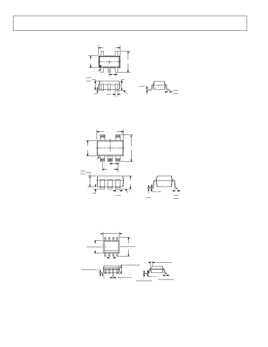
OUTLINE DIMENSIONS
COMPLIANT TO JEDEC STANDARDS MO-203AA
2.00 BSC
0.30
0.15
0.10 MAX
1.00
0.90
0.70
SEATING
PLANE
1.10 MAX
0.22
0.08
0.46
0.36
0.26
4
PIN 1
2.10 BSC
0.65 BSC
1.25 BSC
0.10 COPLANARITY
Figure 45. 5-Lead Thin Shrink Small Outline Transistor Package [SC70]
(KS-5)
Dimensions shown in millimeters
PIN 1
1.60 BSC
2.80 BSC
1.90
BSC
0.95 BSC
1
3
4
5
2
0.20
0.08
0.60
0.45
0.30
8°
4°
0.50
0.30
0.10 MAX
SEATING
PLANE
1.00 MAX
0.90
0.87
0.84
COMPLIANT TO JEDEC STANDARDS MO-193AB
2.90 BSC
Figure 46. 5-Lead Thin Small Outline Transistor Package [TSOT]
(UJ-5)
Dimensions shown in millimeters
0.25 (0.0098)
0.17 (0.0067)
1.27 (0.0500)
0.40 (0.0157)
0.50 (0.0196)
0.25 (0.0099)
×
45°
8°
0°
1.75 (0.0688)
1.35 (0.0532)
SEATING
PLANE
0.25 (0.0098)
0.10 (0.0040)
4
1
8
5
5.00 (0.1968)
4.80 (0.1890)
4.00 (0.1574)
3.80 (0.1497)
1.27 (0.0500)
BSC
6.20 (0.2440)
5.80 (0.2284)
0.51 (0.0201)
0.31 (0.0122)
COPLANARITY
0.10
CONTROLLING DIMENSIONS ARE IN MILLIMETERS; INCH DIMENSIONS
(IN PARENTHESES) ARE ROUNDED-OFF MILLIMETER EQUIVALENTS FOR
REFERENCE ONLY AND ARE NOT APPROPRIATE FOR USE IN DESIGN
COMPLIANT TO JEDEC STANDARDS MS-012AA
Figure 47. 8-Lead Standard Small Outline Package [SOIC]
Narrow Body (R-8)
Dimensions shown in millimeters and (inches)
ADR01/ADR02/ADR03/ADR06
Rev. F | Page 19 of 20
ORDERING GUIDES
ADR01 ORDERING GUIDE
Output
Voltage
Initial
Accuracy
Temperature
Coefficient
Model
V
O
(V)
(mV)
(%)
(ppm/°C)
Package
Description
Package
Option
Top
Mark
1
Number of
Parts per
Reel/Tray
Temperature
Range (°C)
ADR01AR 10
10
0.1
10
SOIC-8
R-8
ADR01
98
40
to
+125
ADR01AR-REEL7 10
10
0.1
10
SOIC-8
R-8
ADR01
1,000
40
to
+125
ADR01BR 10
5
0.05
3
SOIC-8
R-8
ADR01
98
40
to
+125
ADR01BR-REEL7 10
5
0.05
3
SOIC-8
R-8
ADR01
1,000
40
to
+125
ADR01AUJ-REEL7 10 10
0.1
25
TSOT-23-5
UJ-5
R8A
3,000 40
to
+125
ADR01AUJ-R2 10
10
0.1
25 TSOT-23-5
UJ-5
R8A
250
40
to
+125
ADR01BUJ-REEL7 10
5
0.05
9
TSOT-23-5
UJ-5
R8B
3,000 40
to
+125
ADR01BUJ-R2 10
5
0.05
9
TSOT-23-5
UJ-5
R8B
250
40
to
+125
ADR01AKS-REEL7 10 10
0.1
25
SC70 KS-5
R8A
3,000 40
to
+125
ADR01AKS-R2 10
10
0.1
25 SC70
KS-5
R8A
250
40
to
+125
ADR01BKS-REEL7 10
5
0.05
9
SC70 KS-5
R8B
3,000 40
to
+125
ADR01BKS-R2 10
5
0.05
9
SC70
KS-5
R8B
250
40
to
+125
ADR01CRZ
2
10 10
0.1
40
SOIC-8 R-8 ADR01
98
40
to
+125
ADR01CRZ-REEL
2
10 10
0.1
40
SOIC-8 R-8 ADR01
2,500 40
to
+125
ARR01NBC 10
5
0.05
10
(Typ)
Dice
360
1
First line shows part number ADR01; second line shows A or B for the grade, with the YYMM date code; third line shows the lot number.
2
Z = Pb-free part.
ADR02 ORDERING GUIDE
Output
Voltage
Initial
Accuracy
Temperature
Coefficient
Model
V
O
(V)
(mV)
(%)
(ppm/°C)
Package
Description
Package
Option
Top
Mark
1
Number of
Parts per
Reel/Tray
Temperature
Range (°C)
ADR02AR 5
5
0.1
10
SOIC-8
R-8
ADR02
98
40
to
+125
ADR02AR-REEL 5
5
0.1
10
SOIC-8
R-8
ADR02
1,000
40
to
+125
ADR02AR-REEL7 5 5
0.1
10
SOIC-8
R-8
ADR02
1,000
40
to
+125
ADR02ARZ
2
5 5
0.1
10
SOIC-8
R-8
ADR02
98
40
to
+125
ADR02ARZ-REEL
2
5 5
0.1
10
SOIC-8
R-8
ADR02
2,500 40
to
+125
ADR02BR 5
3
0.06
3
SOIC-8
R-8
ADR02
98
40
to
+125
ADR02BR-REEL7 5 3
0.06
3
SOIC-8
R-8
ADR02
1,000
40
to
+125
ADR02AUJ-REEL7 5 5
0.1
25
TSOT-23-5
UJ-5
R9A
3,000 40
to
+125
ADR02AUJ-R2 5
5
0.1
25 TSOT-23-5
UJ-5
R9A
250
40
to
+125
ADR02BUJ-REEL7 5 3
0.06
9
TSOT-23-5
UJ-5
R9B
3,000 40
to
+125
ADR02BUJ-R2 5
3
0.06
9
TSOT-23-5
UJ-5
R9B
250
40
to
+125
ADR02AKS-REEL7 5 5
0.1
25
SC70 KS-5
R9A
3,000 40
to
+125
ADR02AKS-R2 5
5
0.1
25 SC70
KS-5
R9A
250
40
to
+125
ADR02BKS-REEL7 5 3
0.06
9
SC70 KS-5
R9B
3,000 40
to
+125
ADR02BKS-R2 5
3
0.06
9
SC70
KS-5
R9B
250
40
to
+125
ADR02CRZ
2
5.0 5
0.1
40
SOIC-8 R-8 ADR02
98
40
to
+125
ADR02CRZ-REEL
2
5.0 5
0.1
40
SOIC-8 R-8 ADR02
2500 40
to
+125
ARR02NBC 5
3
0.06
10
(Typ)
Dice
360
1
First line shows part number ADR02; second line shows A or B for the grade, with the YYMM date code; third line shows the lot number.
2
Z = Pb-free part.
ADR01/ADR02/ADR03/ADR06
Rev. F | Page 20 of 20
ADR03 ORDERING GUIDE
Output
Voltage
Initial
Accuracy
Temperature
Coefficient
Model
V
O
(V)
(mV)
(%)
(ppm/°C)
Package
Description
Package
Option
Top
Mark
1
Number of
Parts per
Reel/Tray
Temperature
Range (°C)
ADR03AR 2.5
5
0.2
10
SOIC-8
R-8
ADR03
98
40
to
+125
ADR03AR-REEL7 2.5
5
0.2
10
SOIC-8
R-8
ADR03
1,000
40
to
+125
ADR03BR 2.5
2.5
0.1
3
SOIC-8
R-8
ADR03
98
40
to
+125
ADR03BR-REEL7 2.5
2.5
0.1
3
SOIC-8 R-8 ADR03
1,000 40
to
+125
ADR03AUJ-REEL7 2.5
5
0.2
25
TSOT-23-5
UJ-5
RFA
3,000 40
to
+125
ADR03AUJ-R2 2.5
5
0.2
25 TSOT-23-5
UJ-5
RFA
250
40
to
+125
ADR03BUJ-REEL7 2.5
2.5
0.1
9
TSOT-23-5
UJ-5
RFB
3,000 40
to
+125
ADR03BUJ-R2 2.5
2.5
0.1
9
TSOT-23-5
UJ-5
RFB
250
40
to
+125
ADR03AKS-REEL7 2.5
5
0.2
25
SC70 KS-5
RFA
3,000 40
to
+125
ADR03AKS-R2 2.5
5
0.2
25 SC70
KS5
RFA
250
40
to
+125
ADR03BKSREEL7 2.5
2.5
0.1
9
SC70 KS5
RFB
3,000 40
to
+125
ADR03BKSR2 2.5
2.5
0.1
9
SC70
KS5
RFB
250
40
to
+125
ADR03BKSZREEL7
2
2.5 2.5
0.1
9
SC70
KS5 RFB 3,000 40
to
+125
ADR03CRZ
2
2.5 5
0.1
40
SOIC-8 R-8 ADR02
98
40
to
+125
ADR03CRZ-REEL
2
2.5 5
0.1
40
SOIC-8 R-8 ADR02
2500 40
to
+125
1
First line shows part number ADR03; second line shows A or B for the grade, with the YYMM date code; third line shows the lot number.
2
Z = Pb-free part.
ADR06 ORDERING GUIDE
Output
Voltage
Initial
Accuracy
Temperature
Coefficient
Model
V
O
(V)
(mV)
(%)
(ppm/°C)
Package
Description
Package
Option
Top
Mark
1
Number of
Parts per
Reel/Tray
Temperature
Range (°C)
ADR06AR 3.0
6
0.2
10
SOIC-8
R-8
ADR06
98
40
to
+125
ADR06AR-REEL7 3.0
3
0.2
10
SOIC-8
R-8
ADR06
1,000
40
to
+125
ADR06BR 3.0
6
01
3
SOIC-8
R-8
ADR06
98
40
to
+125
ADR06BR-REEL7 3.0
3
0.1
3
SOIC-8 R-8 ADR06
1,000 40
to
+125
ADR06AUJ-R2 3.0
6
0.2
25 TSOT-23-5
UJ-5
RWA
250
40
to
+125
ADR06AUJ-REEL7 3.0
6
0.2
25
TSOT-23-5
UJ-5
RWA
3,000 40
to
+125
ADR06BUJR2 3.0
3
0.1
9
TSOT-23-5
UJ-5
RWB
250
40
to
+125
ADR06BUJ-REEL7 3.0
3
0.1
9
TSOT-23-5
UJ-5
RWB
3,000 40
to
+125
ADR06AKS-R2 3.0
6
0.2
25 SC70
KS-5
RWA
250
40
to
+125
ADR06AKS-REEL7 3.0
6
0.2
25
SC70 KS5
RWA
3,000 40
to
+125
ADR06BKS-R2 3.0
3
0.1
9
SC70
KS-5
RWB
250
40
to
+125
ADR06BKSREEL7 3.0
3
0.1
9
SC70 KS5
RWB
3,000 40
to
+125
ADR06CRZ
2
3.0 6
0.2
40
SOIC-8 R-8 ADR06
98
40
to
+125
ADR06CRZ-REEL
2
3.0 6
0.2
40
SOIC-8 R-8 ADR06
2500 40
to
+125
1
First line shows part number ADR06; second line shows A or B for the grade, with the YYMM date code; third line shows the lot number.
2
Z = Pb-free part.
© 2004 Analog Devices, Inc. All rights reserved. Trademarks and
registered trademarks are the property of their respective owners.
C0274707/04(F)
Document Outline
- FEATURES
- APPLICATIONS
- SELECTION GUIDE
- PIN CONFIGURATIONS
- GENERAL DESCRIPTION
- þÿ
- þÿ
- þÿ
- þÿ
- þÿ
- þÿ
- þÿ