 | –≠–ª–µ–∫—Ç—Ä–æ–Ω–Ω—ã–π –∫–æ–º–ø–æ–Ω–µ–Ω—Ç: ADR280 | –°–∫–∞—á–∞—Ç—å:  PDF PDF  ZIP ZIP |
ƒÓÍÛÏÂÌÚýˆËˇ Ë ÓÔËÒýÌˡ www.docs.chipfind.ru
Information furnished by Analog Devices is believed to be accurate and
reliable. However, no responsibility is assumed by Analog Devices for its
use, nor for any infringements of patents or other rights of third parties
that may result from its use. No license is granted by implication or oth-
erwise under any patent or patent rights of Analog Devices. Trademarks
and registered trademarks are the property of their respective companies.
One Technology Way, P.O. Box 9106, Norwood, MA 02062-9106, U.S.A.
Tel: 781/329-4700
www.analog.com
Fax: 781/326-8703 © 2003 Analog Devices, Inc. All rights reserved.
ADR280
1.2 V Ultralow Power
High PSRR Voltage Reference
FEATURES
1.2 V Precision Output
Excellent Line Regulation, 2 ppm/V Typical
High Power Supply Ripple Rejection, ≠80 dB at 220 Hz
Ultralow Power, Supply Current 16 A Maximum
Temperature Coefficient, 40 ppm/
o
C Maximum
Low Noise, 12.5 nV/
˜Hz Typical
Operating Supply Range, 2.4 V to 5.5 V
Compact 3-Lead SOT-23 and SC70 Packages
APPLICATIONS
GSM, GPRS, 3G Mobile Stations
Portable Battery-Operated Electronics
Low Voltage Converter References
Wireless Devices
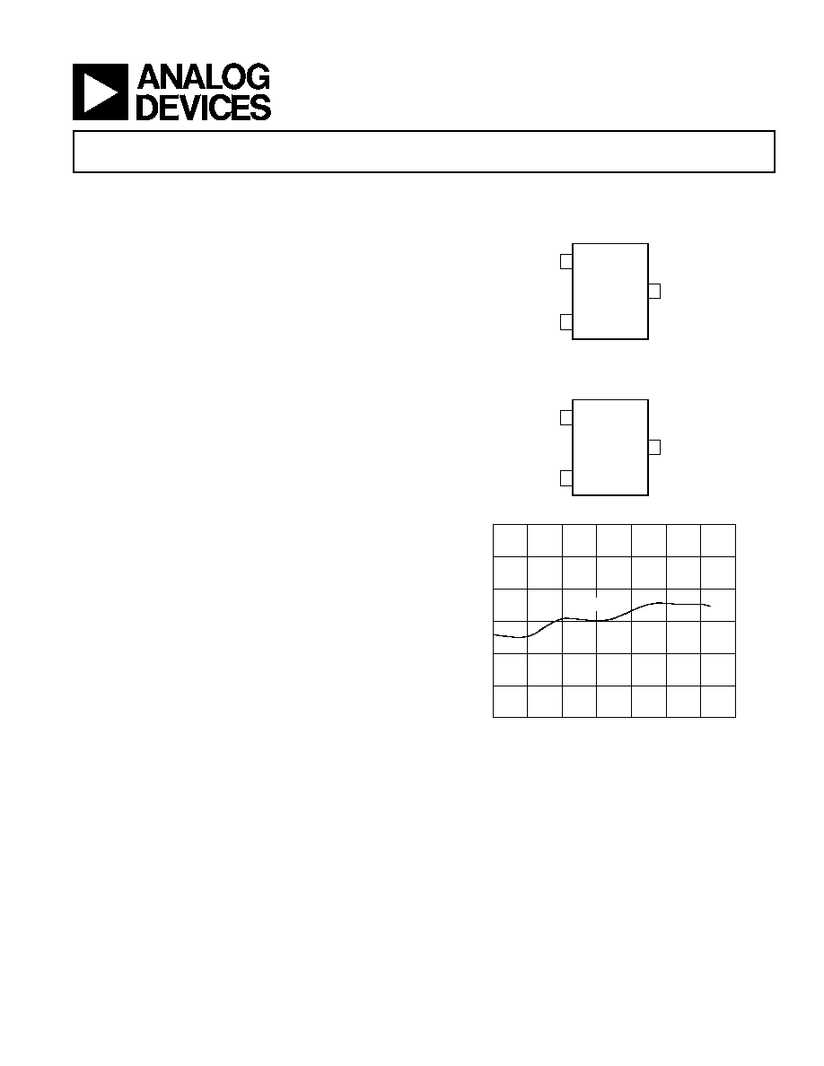
PIN CONFIGURATIONS
3-Lead SOT-23
(RT Suffix)
V
OUT
V+ 1
2
3
ADR280
V≠
3-Lead SC70
(KS Suffix)
V+
V
OUT
1
2
3
ADR280
V≠
TEMPERATURE (C)
15
≠15
≠40
100
≠20
LINE REGUL
A
T
ION (ppm/V
)
0
20
40
60
80
≠10
≠5
0
5
10
3V TO 5V
Figure 1. Line Regulation vs. Temperature
GENERAL DESCRIPTION
The ADR280 is a 1.2 V band gap core reference with excellent
line regulation and power supply rejection designed specifically
for applications experiencing heavy dynamic supply variations,
such as data converter references in GSM, GPRS, and 3G
mobile station applications. Devices such as the AD6535, which
has an analog baseband IC with on-board baseband and audio
codecs, voltage regulators, and battery charger, rely on the
ADR280's ability to reject input battery voltage variations during
RF power amplifier activity.
In addition to mobile stations, the ADR280 is suitable for a
variety of general-purpose applications. Most band gap refer-
ences include internal gain for specific outputs, which simplifies
the user's design but compromises on the cost, form factor, and
flexibility. The ADR280, on the other hand, optimizes the band
gap core voltage and allows users to tailor the voltage, current, or
transient response by simply adding their preferred op amps.
The ADR280 operates on a wide supply voltage range from 2.4 V
to 5.5 V. It is available in compact 3-lead SOT-23 and SC70
packages. The device is specified over the extended industrial
temperature range of ≠40∞C to +85∞C.
REV. A
≠2≠
ADR280≠SPECIFICATIONS
≠3≠
Typical Performance Characteristics≠ADR280
ORDERING GUIDE
Temperature
Package
Package
Top
Output
Number of
Model
Range
Description
Option
Mark
Voltage (V) Parts per Reel
ADR280ART-R2
≠40∞C to +85∞C
SOT-23
RT-3
RBA
1.200
250
ADR280ART-REEL7
≠40∞C to +85∞C
SOT-23
RT-3
RBA
1.200
3,000
ADR280ART-REEL
≠40∞C to +85∞C
SOT-23
RT-3
RBA
1.200
10,000
ADR280AKS-R2
≠40∞C to +85∞C
SC70
KS-3
RBA
1.200
250
ADR280AKS-REEL7
≠40∞C to +85∞C
SC70
KS-3
RBA
1.200
3,000
ADR280AKS-REEL
≠40∞C to +85∞C
SC70
KS-3
RBA
1.200
10,00
0
(V
IN
= 2.55 V to 5.5 V, T
A
= 25∞C, unless otherwise noted.)
Parameter Symbol Conditions
Min
Typ
1
Max
Unit
Output Voltage
2
V
OUT
1.195
1.200
1.205
V
Temperature Coefficient TCVo 0∞C < T
A
< 50∞C
5
20
ppm/
o
C
≠40∞C < T
A
< +85∞C
10
40
ppm/
o
C
Line Regulation V
OUT
/V
IN
2.55 V < V
IN
< 5.5 V, No Load
2
12
ppm/V
Supply Current I
IN
2.4 V < V
IN
< 5.5 V, No Load
10
16
µA
Ground Current I
GND
V≠ Grounded, I
LOAD
= 10 µA
12
20
µA
Input Voltage Range V
IN
2.4
5.5
V
Operating Temperature Range T
A
≠40
+85
∞C
Nominal Load Capacitance C
OUT
1
µF
Output Noise Voltage V
N
f = 10 Hz to 10 kHz
12.5
µVrms
Output Noise Density e
N
f = 400 kHz
12.5
nV/
˜Hz
Power Supply Ripple Rejection
3
PSRR I
LOAD
= 10 µA
≠80
dB
Start-Up Time t
ON
2
ms
NOTES
1
Typical values represent average readings taken at room temperature.
2
Conditions: 2.4 V < V
IN
< 5.5 V, 0 µA < I
OUT
< 10 µA, ≠40∞C < T
A
< +85∞C.
3
Power supply ripple rejection measurement applies to a changing input voltage (V
IN
) waveform with a nominal 3.6 V baseline that drops to a 3 V value for
380 µs at a 4.6 ms repetition rate.
Specifications subject to change without notice.
ELECTRICAL CHARACTERISTICS
ABSOLUTE MAXIMUM RATINGS
1, 2
Supply Voltage . . . . . . . . . . . . . . . . . . . . . . . . . . . . . . . . . . . 6 V
Storage Temperature Range . . . . . . . . . . . . . . ≠65∞C to +150∞C
Operating Temperature Range . . . . . . . . . . . . . ≠40∞C to +85∞C
Junction Temperature Range . . . . . . . . . . . . . . ≠65∞C to +150∞C
Lead Temperature Range (Soldering, 60 Sec) . . . . . . . . . .300∞C
NOTES
1
Stresses above those listed under Absolute Maximum Ratings may cause permanent
damage to the device. This is a stress rating only and functional operation of the
device at these or any other conditions above those listed in the operational sections
THERMAL RESISTANCE
Package Type
JA
*
JC
Unit
SOT-23 230
146 ∞C/W
SC70 376
102 ∞C/W
*
JA
is specified for the worst-case conditions, i.e.,
JA
is specified for device sol-
dered in circuit board for surface-mount packages.
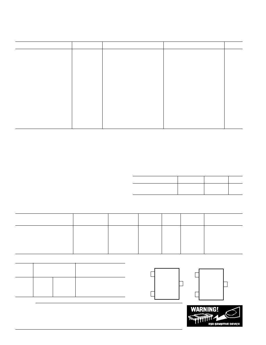
PIN FUNCTION DESCRIPTIONS
Mnemonic
Pin No. SOT-23
SC70 Description
1 V+
V
OUT
High Supply Voltage Input
2 V
OUT
V+ Output Voltage
3 V≠
V≠ Low Supply Voltage Input
PIN CONFIGURATIONS
CAUTION
ESD (electrostatic discharge) sensitive device. Electrostatic charges as high as 4000 V readily accumulate
on the human body and test equipment and can discharge without detection. Although the ADR280
features proprietary ESD protection circuitry, permanent damage may occur on devices subjected to high
energy electrostatic discharges. Therefore, proper ESD precautions are recommended to avoid performance
degradation or loss of functionality.
SOT-23
V
OUT
V+ 1
2
3
ADR280
V≠
SC70
V+
V
OUT
1
2
3
ADR280
V≠
of this specification is not implied. Exposure to absolute maximum rating conditions
for extended periods may affect device reliability.
2
Absolute Maximum Ratings apply at 25∞C, unless otherwise noted.
REV. A
REV. A
≠2≠
ADR280≠SPECIFICATIONS
≠3≠
Typical Performance Characteristics≠ADR280
TEMPERATURE (C)
1.20225
≠40
100
≠20
V
OU
T
(V)
0
20
40
60
80
NO LOAD
1.20200
1.20175
1.20150
1.20125
1.20100
1.20075
1.20050
1.20025
1.20000
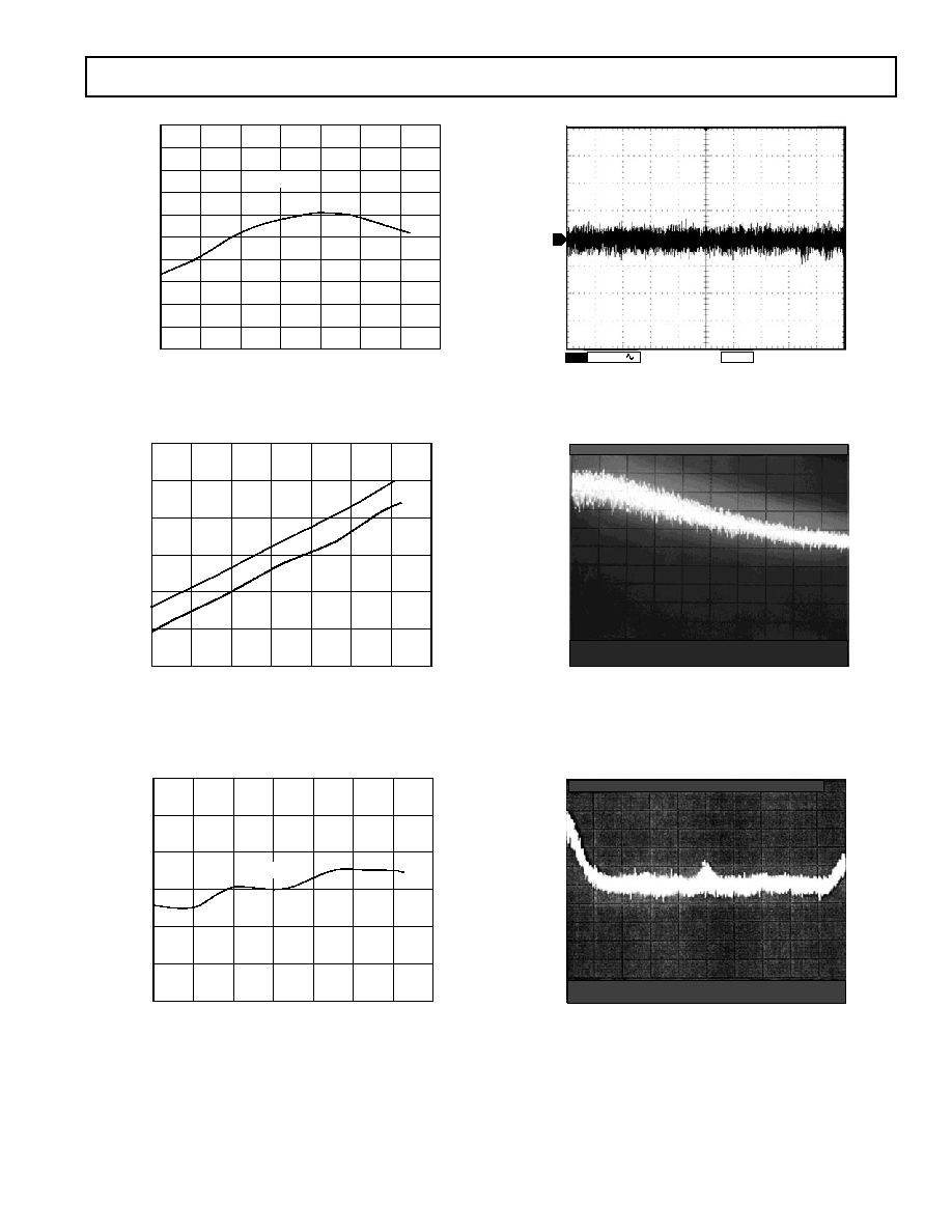
TPC 1. V
OUT
vs. Temperature
TEMPERATURE (C)
≠40
100
≠20
I
IN
(
A)
0
20
40
60
80
V
IN
= 5V
15
14
13
12
11
10
9
V
IN
= 3V
TPC 2. Supply Current vs. Temperature
TEMPERATURE (C)
15
≠15
≠40
100
≠20
LINE REGUL
A
T
ION (ppm/V
)
0
20
40
60
80
≠10
≠5
0
5
10
3V TO 5V
TPC 3. Line Regulation vs. Temperature
Ch1
50.0V
M 1.00 s
1
TPC 4. Noise Voltage Peak-to-Peak 10 Hz to 10 kHz
≠100
≠80
≠60
≠40
NOISE POWER DENSITY (dBm
)
10.0
7.5
5.0
2.5
0
FREQUENCY (kHz)
TPC 5. Output Noise Density Plot
(V
IN
= 3.6 V, C
OUT
= 1 µF, C
IN
= 1 µF)
10dB/DIV
≠40dB
0Hz
100kHz
TPC 6. Voltage Noise Density 0 Hz to 100 kHz
REV. A
REV. A
ADR280
≠4≠
ADR280
≠5≠
THEORY OF OPERATION
The ADR280 provides the basic core 1.2 V band gap reference.
It contains two NPN transistors, Q9 and Q17, with their emitter
areas scaled in a fixed ratio. The difference in their Vbes produces
a PTAT (proportional to absolute temperature) voltage that
cancels the CTAT (complementary to absolute temperature) Q9
Vbe voltage. As a result, a core band gap voltage that is almost a
constant 1.2 V over temperature is generated (see Figure 2). Preci-
sion laser trimming of the internal resistors and other proprietary
circuit techniques are used to enhance the initial accuracy, tem-
perature curvature, and temperature drift performance.
R1
R3
R5
R7
R9
Q17
Q9
Q18
R8
Q3
R6
Q5
Q6
R4
Q1
PNP3
R2
R12
Q2
Q10
R13 C1
Q7
R10
R11
V≠
V+
V
OUT
I1
Figure 2. Simplified Architecture
t
S
1.2
1.0
0.8
0.6
0.4
0.2
0
2
4
6
8
10
12
14
16
18
20
0
V
OL
T
A
GE (V)
TIME (ms)
TPC 7. Settling Time
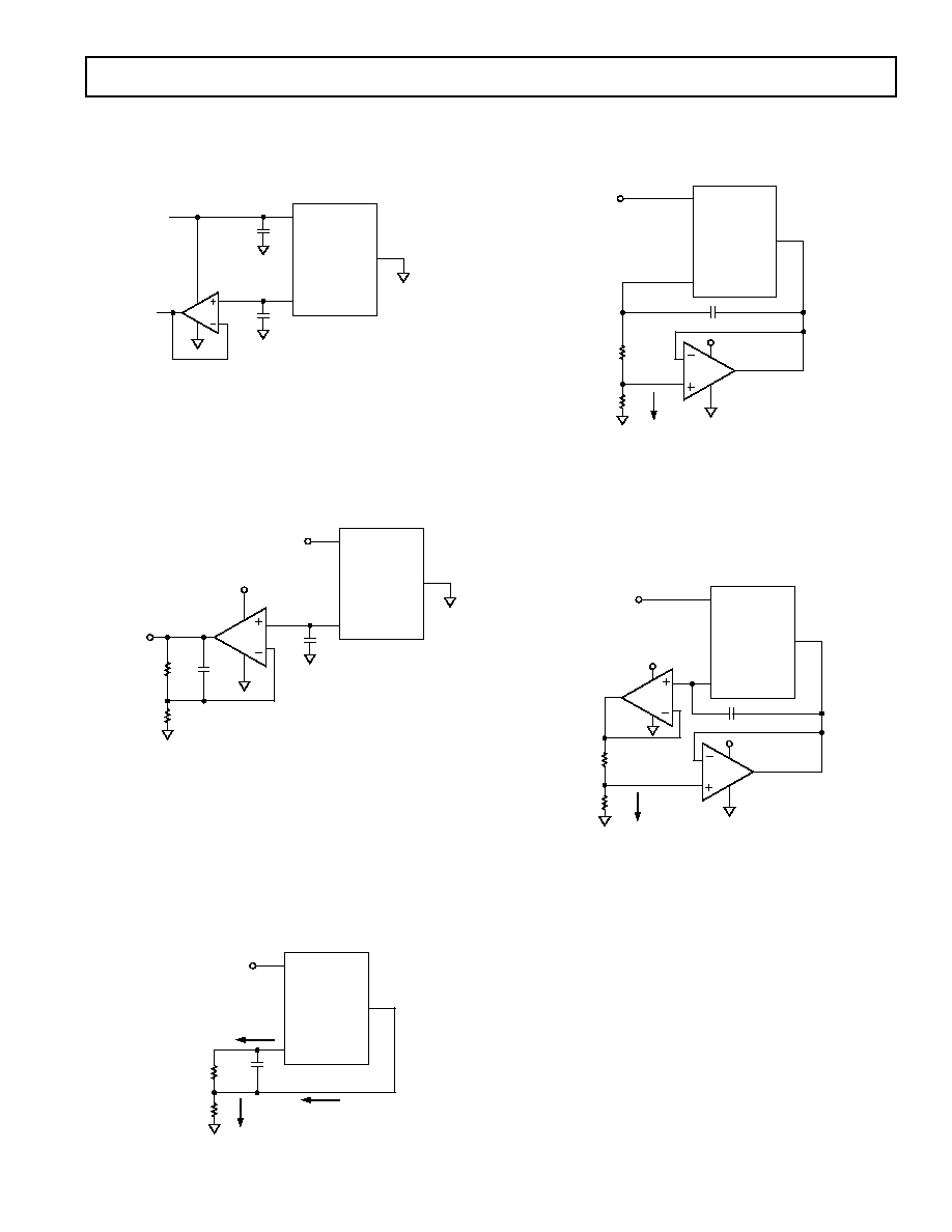
APPLICATIONS
The ADR280 should be decoupled with a 0.1 µF ceramic cap at
the output for optimum stability. It is also good practice to
include 0.1 µF ceramic caps at the IC supply pin. These capaci-
tors should be mounted close to their respective pins (see Figure 3).
V+
V
OUT
0.1F
0.1F
V≠
ADR280
Figure 3. Basic Configuration
The low supply voltage input pin V≠ can be elevated above
ground; a 1.2 V differential voltage can therefore be established
above V≠ (see Figure 4).
V+
V
OUT
0.1F
0.1F
V≠
ADR280
5V
1.2V
2.5V
Figure 4. Floating References
REV. A
REV. A
ADR280
≠4≠
ADR280
≠5≠
The ADR280 provides the core 1.2 V band gap voltage and is
able to drive a maximum load of only 100 µA. Users can simply
buffer the output for high current or sink/source current applica-
tions, such as ADC or LCD driver references (see Figure 5).
V+
V
OUT
0.1F
0.1F
V≠
ADR280
V
OUT
U1
U2
U2 = AD8541, SC70
AD8601, SOT-23-5
Figure 5. Buffered Output
Users can also tailor any specific need for voltage and dynamics
with an external op amp and discrete components (see Figure 5).
Depending on the specific op amp and PCB layout, it may be
necessary to add a compensation capacitor, C2, to prevent gain
peaking and oscillation. The exact value of C2 needed requires
some trial and error but usually falls in the range of a few pF.
V+
V
OUT
0.1F
V≠
ADR280
U1
5V
5V
1.2V
U2
1.8V
R1
R2
60k 0.1%
120k 0.1%
C2
2.2pF
V+
V≠
AD8541
V
O
C1
Figure 6. 1.8 V Reference
LOW COST, LOW POWER CURRENT SOURCE
Because of its low power characteristics, the ADR280 can be
converted to a current source with just a setting resistor. In addi-
tion to the ADR280 current capability, the supply voltage and the
load limit the maximum current. The circuit in Figure 7 produces
100 µA with 2 V compliance at 5 V supply. The load current is
the sum of I
SET
and I
GND
. I
GND
will increase slightly with load; an
R
SET
of 13.6 k yields 100 µA of load current.
V+
V
OUT
0.1F
V≠
ADR280
U1
5V
1.2V
13.6k
C1
R
SET
RL 1k I
L
100A
I
GND
I
L
= I
SET
+ I
GND
I
SET
+
≠
Figure 7. Low Cost Current Source
Precision Low Power Current Source
By adding a buffer to redirect the I
GND
in Figure 8, a current can
be precisely set by R
SET
with the equation I
L
= 1.2 V/R
SET
.
V+
V
OUT
0.1F
V≠
ADR280
U1
5V
C2
R
SET
RL 1k
I
L
100A
I
L
= 1.2V/R
SET
V+
V≠
5V
U2
12k
AD8541
Figure 8. Precision Low Power Current Source
Boosted Current Source
Adding one more buffer to the previous circuit boosts the current
to the level that is limited only by the buffer U2 current handling
capability (see Figure 9).
V+
V
OUT
0.1F
V≠
ADR280
U1
5V
C1
R
SET
230
RL
500
I
L
5mA
I
L
= 1.2V/R
SET
V+
V≠
5V
U3
V+
V≠
5V
U2
U2 = U3 = AD8542, AD822
1.2V
+
≠
Figure 9. Precision Current Source
REV. A
REV. A
ADR280
≠6≠
ADR280
≠7≠
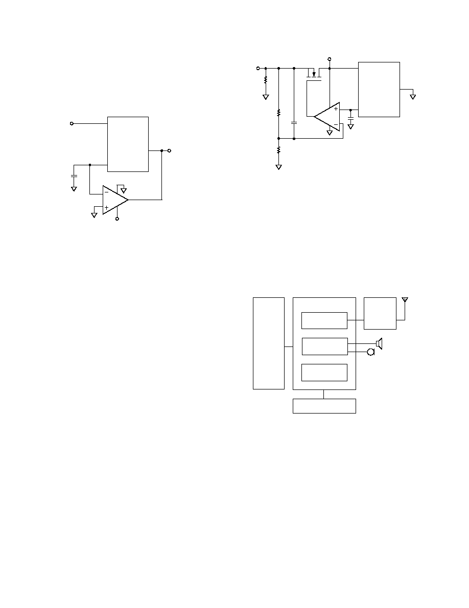
Negative Reference
A negative reference can be precisely configured without using
any expensive tight tolerance resistors, as shown in Figure 10.
The voltage difference between V
OUT
and V≠ is 1.2 V. Since V
OUT
is at virtual ground, U2 will close the loop by forcing the V≠ pin
to be the negative reference output.
V+
V
OUT
0.1F
V≠
ADR280
U1
+5V
V+
V≠
≠2.7V
AD8541
≠1.2V
≠V
REF
U2
C1
Figure 10. Negative Reference
Boosted Reference with Scalable Output
A precision user defined output with boosted current capabil-
ity can be implemented with the circuit shown in Figure 11. In
this circuit, U2 forces V
O
to be equal to V
REF
(1 + R2/R1) by
regulating the turn-on of M1; the load current is therefore fur-
nished by the 5 V supply. For higher output voltage, U2 must
be changed and the supply voltage of M1 and U2 must also be
elevated and separated from the U1 input voltage. In this config-
uration, a 100 mA load is achievable at a 5 V supply. The higher
the supply voltage, the lower the current handling is because of
the heat generated on the MOSFET. For heavy capacitive loads,
additional buffering is needed at the output to enhance the
transient response.
V+
V
OUT
V≠
ADR280
U1
5V
V+
V≠
U2
R1
R2
RL
25
V
O
10.8k 0.1%
10k 0.1%
C2
1pF
1.2V
AD8541
0.1F
C1
M1
2.5V/100mA
M1 = FDB301N, 2N7000, 2N7002, OR EQUIVALENT
Figure 11. 2.5 V Boosted Reference
GSM and 3G Mobile Station Applications
The ADR280 voltage reference is ideal for use with analog base-
band ICs in GSM and 3G mobile station applications. Figure 12
illustrates the use of the ADR280 with the AD6535 GSM analog
baseband. The AD6535 provides all of the data converters and
power management functions needed to implement a GSM
mobile station, including baseband and audio codecs, voltage
regulators, and a battery charger. Besides low current consump-
tion and a small footprint, the ADR280 is optimized for excellent
power supply rejection ratio (PSRR) necessary for optimum
AD6535 device performance when the main battery voltage
fluctuates during RF power amplifier activity.
DIGITAL
BASEBAND
AD6535 ANALOG
BASEBAND
BASEBAND CODEC
AUDIO CODEC
POWER
MANAGEMENT
RADIO
ADR280
VOLTAGE REFERENCE
Figure 12. GSM Mobile Station Application
REV. A
REV. A
ADR280
≠6≠
ADR280
≠7≠
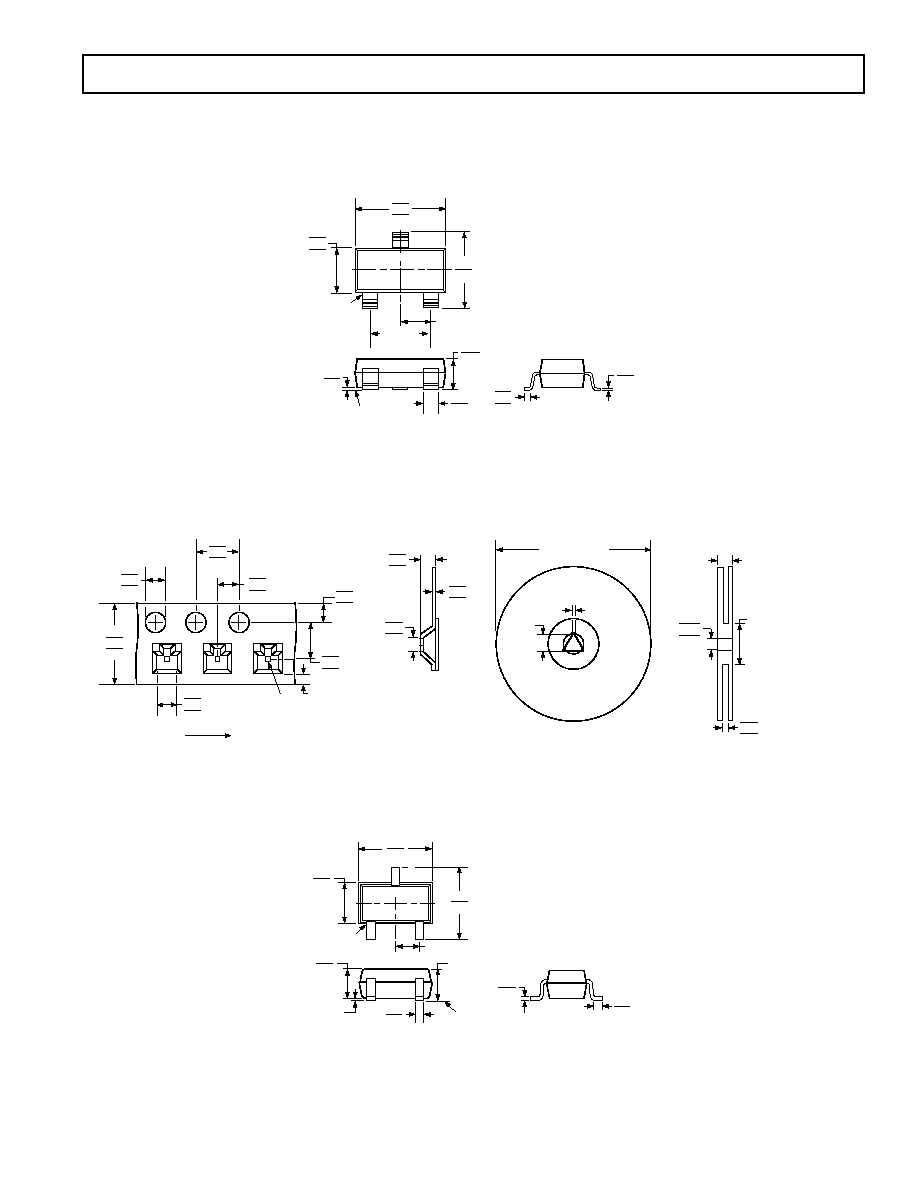
OUTLINE DIMENSIONS
3-Lead Small Outline Transistor Package [SOT-23]
(RT-3)
Dimensions shown in millimeters
3.04
2.90
2.80
PIN 1
1.40
1.30
1.20
2.64
2.10
1.90 BSC
1
2
3
SEATING
PLANE
1.12
0.89
0.10
0.01
0.50
0.30
0.20
0.08
0.60
0.50
0.40
0.95 BSC
COMPLIANT TO JEDEC STANDARDS TO-236AB
Tape and Reel Dimensions
(RT-3)
Dimensions shown in millimeters
4.10
4.00
3.90
1.55
1.50
1.50
8.30
8.00
7.70
3.20
3.10
2.90
2.05
2.00
1.95
1.85
1.75
1.65
3.55
3.50
3.45
2.80
2.70
2.60
1.10
1.00
0.90
0.35
0.30
0.25
13.20
13.00
12.80
9.90
8.40
8.40
20.20
MIN
1.50 MIN
7" REEL 100.00
OR
13" REEL 330.00
7" REEL 50.00 MIN
OR
13" REEL 100.00 MIN
14.40 MAX
0.75 MIN
DIRECTION OF UNREELING
1.00 MIN
3-Lead Thin Shrink Small Outline Transistor Package [SC70]
(KS-3)
Dimensions shown in millimeters
0.40
0.25
0.10 MAX
1.00
0.80
SEATING
PLANE
1.10 MAX
0.18
0.10
0.30
0.10
2
1
3
PIN 1
0.65 BSC
0.10 COPLANARITY
2.20
1.80
2.40
1.80
1.35
1.15
REV. A
REV. A

C03065≠0≠
6
/03(A)
≠8≠
ADR280
Revision History
Location Page
6/03--Data Sheet changed from REV. 0 to REV. A.
Added SC70 package . . . . . . . . . . . . . . . . . . . . . . . . . . . . . . . . . . . . . . . . . . . . . . . . . . . . . . . . . . . . . . . . . . . . . . . . . . . . . . . Universal
Changes to FEATURES . . . . . . . . . . . . . . . . . . . . . . . . . . . . . . . . . . . . . . . . . . . . . . . . . . . . . . . . . . . . . . . . . . . . . . . . . . . . . . . . . . . 1
Changes to GENERAL DESCRIPTION . . . . . . . . . . . . . . . . . . . . . . . . . . . . . . . . . . . . . . . . . . . . . . . . . . . . . . . . . . . . . . . . . . . . . . 1
Changes to SPECIFICATIONS . . . . . . . . . . . . . . . . . . . . . . . . . . . . . . . . . . . . . . . . . . . . . . . . . . . . . . . . . . . . . . . . . . . . . . . . . . . . . 2
Changes to ORDERING GUIDE . . . . . . . . . . . . . . . . . . . . . . . . . . . . . . . . . . . . . . . . . . . . . . . . . . . . . . . . . . . . . . . . . . . . . . . . . . . 2
Changes to TPCs 4, 6, and 7 . . . . . . . . . . . . . . . . . . . . . . . . . . . . . . . . . . . . . . . . . . . . . . . . . . . . . . . . . . . . . . . . . . . . . . . . . . . . . . . . 3
Updated SOT-23 OUTLINE DIMENSIONS . . . . . . . . . . . . . . . . . . . . . . . . . . . . . . . . . . . . . . . . . . . . . . . . . . . . . . . . . . . . . . . . . . 7
REV. A
Document Outline
- FEATURES
- APPLICATIONS
- GENERAL DESCRIPTION
- SPECIFICATIONS
- ABSOLUTE MAXIMUM RATINGS
- THERMAL RESISTANCE
- ORDERING GUIDE
- PIN FUNCTION DESCRIPTIONS
- PIN CONFIGURATIONS
- Typical Performance Characteristics
- THEORY OF OPERATION
- APPLICATIONS
- LOW COST, LOW POWER CURRENT SOURCE
- Precision Low Power Current Source
- Boosted Current Source
- Negative Reference
- Boosted Reference with Scalable Output
- GSM and 3G Mobile Station Applications
- OUTLINE DIMENSIONS
- Revision History