Äîêóìåíòàöèÿ è îïèñàíèÿ www.docs.chipfind.ru
REV. B
Information furnished by Analog Devices is believed to be accurate and
reliable. However, no responsibility is assumed by Analog Devices for its
use, nor for any infringements of patents or other rights of third parties
which may result from its use. No license is granted by implication or
otherwise under any patent or patent rights of Analog Devices.
a
ADSP-21065L
One Technology Way, P.O. Box 9106, Norwood, MA 02062-9106, U.S.A.
Tel: 781/329-4700
World Wide Web Site: http://www.analog.com
Fax: 781/326-8703
© Analog Devices, Inc., 2000
DSP Microcomputer
SUMMARY
High Performance Signal Computer for Communica-
tions, Audio, Automotive, Instrumentation and
Industrial Applications
Super Harvard Architecture Computer (SHARC
®
)
Four Independent Buses for Dual Data, Instruction,
and I/O Fetch on a Single Cycle
32-Bit Fixed-Point Arithmetic; 32-Bit and 40-Bit Floating-
Point Arithmetic
544 Kbits On-Chip SRAM Memory and Integrated I/O
Peripheral
I
2
S Support, for Eight Simultaneous Receive and Trans-
mit Channels
KEY FEATURES
66 MIPS, 198 MFLOPS Peak, 132 MFLOPS Sustained
Performance
User-Configurable 544 Kbits On-Chip SRAM Memory
Two External Port, DMA Channels and Eight Serial
Port, DMA Channels
SDRAM Controller for Glueless Interface to Low Cost
External Memory (@ 66 MHz)
64M Words External Address Range
12 Programmable I/O Pins and Two Timers with Event
Capture Options
Code-Compatible with ADSP-2106x Family
208-Lead MQFP or 196-Ball Mini-BGA Package
3.3 Volt Operation
Flexible Data Formats and 40-Bit Extended Precision
32-Bit Single-Precision and 40-Bit Extended-Precision IEEE
Floating-Point Data Formats
32-Bit Fixed-Point Data Format, Integer and Fractional,
with Dual 80-Bit Accumulators
Parallel Computations
Single-Cycle Multiply and ALU Operations in Parallel with
Dual Memory Read/Writes and Instruction Fetch
Multiply with Add and Subtract for Accelerated FFT But-
terfly Computation
1024-Point Complex FFT Benchmark: 0.274 ms (18,221
Cycles)
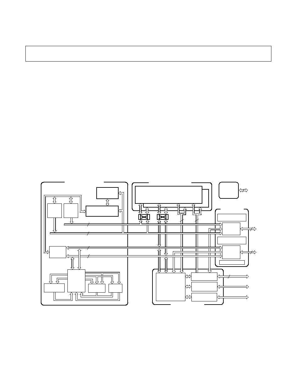
SPORT 1
4
IOP
REGISTERS
(MEMORY MAPPED)
CONTROL,
STATUS, TIMER
&
DATA BUFFERS
I/O PROCESSOR
INSTRUCTION
CACHE
32 48 BIT
DATA
ADDR
TWO INDEPENDENT
DUAL-PORTED BLOCKS
PROCESSOR PORT
I/O PORT
BLOCK 0
BLOCK 1
JTAG
TEST &
EMULATION
7
HOST PORT
ADDR BUS
MUX
IOA
17
IOD
48
MULTIPROCESSOR
INTERFACE
DUAL-PORTED SRAM
EXTERNAL
PORT
DATA BUS
MUX
32
24
24
PM ADDRESS BUS
DM ADDRESS BUS
PM DATA BUS
DM DATA BUS
BUS
CONNECT
(PX)
DATA
REGISTER
FILE
16 40 BIT
BARREL
SHIFTER
ALU
MULTIPLIER
32
48
40
CORE PROCESSOR
DMA
CONTROLLER
PROGRAM
SEQUENCER
DAG2
8 4 24
SDRAM
INTERFACE
(I
2
S)
(2 Rx, 2Tx)
(2 Rx, 2Tx)
(I
2
S)
SPORT 0
DAG1
8 4 32
DATA
DATA
DATA
ADDR
ADDR
ADDR
Figure 1. Functional Block Diagram
SHARC is a registered trademark of Analog Devices, Inc.

REV. B
ADSP-21065L
2
544 Kbits Configurable On-Chip SRAM
Dual-Ported for Independent Access by Core Processor
and DMA
Configurable in Combinations of 16-, 32-, 48-Bit Data and
Program Words in Block 0 and Block 1
DMA Controller
Ten DMA Channels--Two Dedicated to the External Port
and Eight Dedicated to the Serial Ports
Background DMA Transfers at up to 66 MHz, in Parallel
with Full Speed Processor Execution
Performs Transfers Between:
Internal RAM and Host
Internal RAM and Serial Ports
Internal RAM and Master or Slave SHARC
Internal RAM and External Memory or I/O Devices
External Memory and External Devices
Host Processor Interface
Efficient Interface to 8-, 16-, and 32-Bit Microprocessors
Host Can Directly Read/Write ADSP-21065L IOP Registers
Multiprocessing
Distributed On-Chip Bus Arbitration for Glueless, Parallel
Bus Connect Between Two ADSP-21065Ls Plus Host
132 Mbytes/s Transfer Rate Over Parallel Bus
Serial Ports
Independent Transmit and Receive Functions
Programmable 3-Bit to 32-Bit Serial Word Width
I
2
S Support Allowing Eight Transmit and Eight Receive
Channels
Glueless Interface to Industry Standard Codecs
TDM Multichannel Mode with -Law/A-Law Hardware
Companding
Multichannel Signaling Protocol
REV. B
ADSP-21065L
3
GENERAL DESCRIPTION
The ADSP-21065L is a powerful member of the SHARC
family of 32-bit processors optimized for cost sensitive appli-
cations. The SHARC--Super Harvard Architecture--offers the
highest levels of performance and memory integration of any
32-bit DSP in the industry--they are also the only DSP in the
industry that offer both fixed and floating-point capabilities,
without compromising precision or performance.
Fabricated in a high speed, low power CMOS process, 0.35
µm
technology, the ADSP-21065L offers the highest performance
by a 32-bit DSP--66 MIPS (198 MFLOPS). With its on-chip
instruction cache, the processor can execute every instruction in
a single cycle. Table I lists the performance benchmarks for the
ADSP-21065L.
The ADSP-21065L SHARC combines a floating-point DSP
core with integrated, on-chip system features, including a
544 Kbit SRAM memory, host processor interface, DMA con-
troller, SDRAM controller, and enhanced serial ports.
Figure 1 shows a block diagram of the ADSP-21065L, illustrat-
ing the following architectural features:
Computation Units (ALU, Multiplier, and Shifter) with a
Shared Data Register File
Data Address Generators (DAG1, DAG2)
Program Sequencer with Instruction Cache
Timers with Event Capture Modes
On-Chip, dual-ported SRAM
External Port for Interfacing to Off-Chip Memory and
Peripherals
Host Port and SDRAM Interface
DMA Controller
Enhanced Serial Ports
JTAG Test Access Port
Table I. Performance Benchmarks
Benchmark
Timing
Cycles
Cycle Time
15.00 ns
1
1024-Pt. Complex FFT
(Radix 4, with Digit Reverse)
0.274 ns
18221
Matrix Multiply (Pipelined)
[3
× 3] × [3 × 1]
135 ns
9
[4
× 4] × [4 × 1]
240 ns
16
FIR Filter (per Tap)
15 ns
1
IIR Filter (per Biquad)
60 ns
4
Divide Y/X
90 ns
6
Inverse Square Root (1/
x)
135 ns
9
DMA Transfers
264 Mbytes/sec.
ADSP-21000 FAMILY CORE ARCHITECTURE
The ADSP-21065L is code and function compatible with the
ADSP-21060/ADSP-21061/ADSP-21062. The ADSP-21065L
includes the following architectural features of the SHARC
family core.
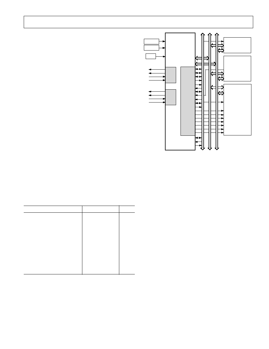
RESET
ADSP-21065L
#1
BMS
ADDR
23-0
DATA
31-0
CONTROL
ADDRESS
DATA
CS
ADDR
DATA
BOOT
EPROM
(OPTIONAL)
ADDR
SDRAM
(OPTIONAL)
DATA
ADDR
DATA
HOST
PROCESSOR
(OPTIONAL)
CLOCK
CS
HBR
HBG
REDY
RD
WR
ACK
SBTS
SW
BR
2
CLKIN
MS
3-0
CPA
CS
RESET
ID
1-0
01
TX0_A
TX0_B
RX0_A
RX0_B
SPORT0
TX1_A
TX1_B
RX1_A
RX1_B
SPORT1
CS
RAS
CAS
DQM
SDCLK
1-0
SDCKE
SDA10
BR
1
RAS
CAS
DQM
CLK
CKE
A10
CONTROL
SDWE
WE
Figure 2. ADSP-21065L Single-Processor System
Independent, Parallel Computation Units
The arithmetic/logic unit (ALU), multiplier, and shifter all
perform single-cycle instructions. The three units are arranged
in parallel, maximizing computational throughput. Single multi-
function instructions execute parallel ALU and multiplier
operations. These computation units support IEEE 32-bit
single-precision floating-point, extended precision 40-bit floating-
point, and 32-bit fixed-point data formats.
Data Register File
A general-purpose data register file is used for transferring data
between the computation units and the data buses, and for
storing intermediate results. This 10-port, 32-register (16 pri-
mary, 16 secondary) register file, combined with the ADSP-
21000 Harvard architecture, allows unconstrained data flow
between computation units and internal memory.
Single-Cycle Fetch of Instruction and Two Operands
The ADSP-21065L features an enhanced Super Harvard Archi-
tecture in which the data memory (DM) bus transfers data and
the program memory (PM) bus transfers both instructions and
data (see Figure 1). With its separate program and data memory
buses, and on-chip instruction cache, the processor can simulta-
neously fetch two operands and an instruction (from the cache),
all in a single cycle.
Instruction Cache
The ADSP-21065L includes an on-chip instruction cache that
enables three-bus operation for fetching an instruction and two
data values. The cache is selective--only the instructions that
fetches conflict with PM bus data accesses are cached. This
allows full-speed execution of core, looped operations such as
digital filter multiply-accumulates and FFT butterfly processing.
Data Address Generators with Hardware Circular Buffers
The ADSP-21065L's two data address generators (DAGs)
implement circular data buffers in hardware. Circular buffers
allow efficient programming of delay lines and other data

REV. B
ADSP-21065L
4
structures required in digital signal processing, and are com-
monly used in digital filters and Fourier transforms. The
ADSP-21065L's two DAGs contain sufficient registers to allow
the creation of up to 32 circular buffers (16 primary register
sets, 16 secondary). The DAGs automatically handle address
pointer wraparound, reducing overhead, increasing perfor-
mance, and simplifying implementation. Circular buffers can
start and end at any memory location.
Flexible Instruction Set
The 48-bit instruction word accommodates a variety of parallel
operations, for concise programming. For example, the ADSP-
21065L can conditionally execute a multiply, an add, a subtract
and a branch, all in a single instruction.
ADSP-21065L FEATURES
The ADSP-21065L is designed to achieve the highest system
throughput to enable maximum system performance. It can be
clocked by either a crystal or a TTL-compatible clock signal.
The ADSP-21065L uses an input clock with a frequency equal
to half the instruction rate--a 33 MHz input clock yields a
15 ns processor cycle (which is equivalent to 66 MHz). Inter-
faces on the ADSP-21065L operate as shown below. Hereafter
in this document, 1x = input clock frequency, and 2x = processor's
instruction rate.
The following clock operation ratings are based on 1x = 33 MHz
(instruction rate/core = 66 MHz):
SDRAM
66 MHz
External SRAM
33 MHz
Serial Ports
33 MHz
Multiprocessing
33 MHz
Host (Asynchronous)
33 MHz
Augmenting the ADSP-21000 family core, the ADSP-21065L
adds the following architectural features:
Dual-Ported On-Chip Memory
The ADSP-21065L contains 544 Kbits of on-chip SRAM,
organized into two banks: Bank 0 has 288 Kbits, and Bank 1 has
256 Kbits. Bank 0 is configured with 9 columns of 2K
× 16 bits,
and Bank 1 is configured with 8 columns of 2K
× 16 bits. Each
memory block is dual-ported for single-cycle, independent ac-
cesses by the core processor and I/O processor or DMA control-
ler. The dual-ported memory and separate on-chip buses allow
two data transfers from the core and one from I/O, all in a
single cycle (see Figure 4 for the ADSP-21065L Memory Map).
On the ADSP-21065L, the memory can be configured as a
maximum of 16K words of 32-bit data, 34K words for 16-bit
data, 10K words of 48-bit instructions (and 40-bit data) or
combinations of different word sizes up to 544 Kbits. All the
memory can be accessed as 16-bit, 32-bit or 48-bit.
While each memory block can store combinations of code and
data, accesses are most efficient when one block stores data,
using the DM bus for transfers, and the other block stores in-
structions and data, using the PM bus for transfers. Using the
DM and PM busses in this way, with one dedicated to each
memory block, assures single-cycle execution with two data
transfers. In this case, the instruction must be available in the
cache. Single-cycle execution is also maintained when one of the
data operands is transferred to or from off-chip, via the ADSP-
21065L's external port.
Off-Chip Memory and Peripherals Interface
The ADSP-21065L's external port provides the processor's
interface to off-chip memory and peripherals. The 64M words,
off-chip address space is included in the ADSP-21065L's uni-
fied address space. The separate on-chip buses--for program
memory, data memory and I/O--are multiplexed at the external
port to create an external system bus with a single 24-bit ad-
dress bus, four memory selects, and a single 32-bit data bus.
The on-chip Super Harvard Architecture provides three bus
performance, while the off-chip unified address space gives
flexibility to the designer.
SDRAM Interface
The SDRAM interface enables the ADSP-21065L to transfer
data to and from synchronous DRAM (SDRAM) at 2x clock
frequency. The synchronous approach coupled with 2x clock
frequency supports data transfer at a high throughput--up to
220 Mbytes/sec.
The SDRAM interface provides a glueless interface with stan-
dard SDRAMs--16 Mb, 64 Mb, and 128 Mb--and includes
options to support additional buffers between the ADSP-21065L
and SDRAM. The SDRAM interface is extremely flexible and
provides capability for connecting SDRAMs to any one of the
ADSP-21065L's four external memory banks.
Systems with several SDRAM devices connected in parallel may
require buffering to meet overall system timing requirements.
The ADSP-21065L supports pipelining of the address and
control signals to enable such buffering between itself and mul-
tiple SDRAM devices.
Host Processor Interface
The ADSP-21065L's host interface provides easy connection to
standard microprocessor buses--8-, 16-, and 32-bit--requiring
little additional hardware. Supporting asynchronous transfers at
speeds up to 1x clock frequency, the host interface is accessed
through the ADSP-21065L's external port. Two channels of
DMA are available for the host interface; code and data trans-
fers are accomplished with low software overhead.
The host processor requests the ADSP-21065L's external bus
with the host bus request (
HBR), host bus grant (HBG), and
ready (REDY) signals. The host can directly read and write the
IOP registers of the ADSP-21065L and can access the DMA
channel setup and mailbox registers. Vector interrupt support
enables efficient execution of host commands.
DMA Controller
The ADSP-21065L's on-chip DMA controller allows zero-
overhead, nonintrusive data transfers without processor inter-
vention. The DMA controller operates independently and
invisibly to the processor core, allowing DMA operations to
occur while the core is simultaneously executing its program
instructions.
DMA transfers can occur between the ADSP-21065L's internal
memory and either external memory, external peripherals, or a
host processor. DMA transfers can also occur between the
ADSP-21065L's internal memory and its serial ports. DMA
transfers between external memory and external peripheral
devices are another option. External bus packing to 16-, 32-, or
48-bit internal words is performed during DMA transfers.
Ten channels of DMA are available on the ADSP-21065L--
eight via the serial ports, and two via the processor's external
port (for either host processor, other ADSP-21065L, memory or

REV. B
ADSP-21065L
5
I/O transfers). Programs can be downloaded to the ADSP-
21065L using DMA transfers. Asynchronous off-chip peripher-
als can control two DMA channels using DMA Request/Grant
lines (
DMAR
1-2,
DMAG
1-2
). Other DMA features include inter-
rupt generation on completion of DMA transfers and DMA
chaining for automatically linked DMA transfers.
Serial Ports
The ADSP-21065L features two synchronous serial ports that
provide an inexpensive interface to a wide variety of digital and
mixed-signal peripheral devices. The serial ports can operate at
1x clock frequency, providing each with a maximum data rate of
33 Mbit/s. Each serial port has a primary and a secondary set of
transmit and receive channels. Independent transmit and receive
functions provide greater flexibility for serial communications.
Serial port data can be automatically transferred to and from
on-chip memory via DMA. Each of the serial ports supports
three operation modes: DSP serial port mode, I
2
S mode (an
interface commonly used by audio codecs), and TDM (Time
Division Multiplex) multichannel mode.
The serial ports can operate with little-endian or big-endian
transmission formats, with selectable word lengths of 3 bits to
32 bits. They offer selectable synchronization and transmit
modes and optional
µ-law or A-law companding. Serial port
clocks and frame syncs can be internally or externally generated.
The serial ports also include keyword and keymask features to
enhance interprocessor communication.
Programmable Timers and General Purpose I/O Ports
The ADSP-21065L has two independent timer blocks, each of
which performs two functions--Pulsewidth Generation and
Pulse Count and Capture.
In Pulsewidth Generation mode, the ADSP-21065L can gener-
ate a modulated waveform with an arbitrary pulsewidth within
a maximum period of 71.5 secs.
In Pulse Counter mode, the ADSP-21065L can measure either
the high or low pulsewidth and the period of an input waveform.
The ADSP-21065L also contains twelve programmable, general
purpose I/O pins that can function as either input or output. As
output, these pins can signal peripheral devices; as input, these
pins can provide the test for conditional branching.
Program Booting
The internal memory of the ADSP-21065L can be booted at
system power-up from an 8-bit EPROM, a host processor, or
external memory. Selection of the boot source is controlled by
the
BMS (Boot Memory Select) and BSEL (EPROM Boot)
pins. Either 8-, 16-, or 32-bit host processors can be used for
booting. For details, see the descriptions of the
BMS and BSEL
pins in the Pin Descriptions section of this data sheet.
Multiprocessing
The ADSP-21065L offers powerful features tailored to multi-
processing DSP systems. The unified address space allows
direct interprocessor accesses of both ADSP-21065L's IOP
registers. Distributed bus arbitration logic is included on-chip
for simple, glueless connection of systems containing a maxi-
mum of two ADSP-21065Ls and a host processor. Master pro-
cessor changeover incurs only one cycle of overhead. Bus lock
allows indivisible read-modify-write sequences for semaphores.
A vector interrupt is provided for interprocessor commands.
Maximum throughput for interprocessor data transfer is
132 Mbytes/sec over the external port.
DEVELOPMENT TOOLS
The ADSP-21065L is supported with a complete set of software
and hardware development tools, including the EZ-ICE
®
In-
Circuit Emulator and development software.
The same EZ-ICE hardware that you use for the ADSP-21060/
ADSP-21062 also fully emulates the ADSP-21065L.
Both the SHARC Development Tools family and the VisualDSP
®
integrated project management and debugging environment
support the ADSP-21065L. The VisualDSP project manage-
ment environment enables you to develop and debug an appli-
cation from within a single integrated program.
The SHARC Development Tools include an easy to use Assem-
bler that is based on an algebraic syntax; an Assembly library/
librarian; a linker; a loader; a cycle-accurate, instruction-level
simulator; a C compiler; and a C run-time library that includes
DSP and mathematical functions.
Debugging both C and Assembly programs with the Visual DSP
debugger, you can:
·
View Mixed C and Assembly Code
·
Insert Break Points
·
Set Watch Points
·
Trace Bus Activity
·
Profile Program Execution
·
Fill and Dump Memory
·
Create Custom Debugger Windows
The Visual IDE enables you to define and manage multiuser
projects. Its dialog boxes and property pages enable you to
configure and manage all of the SHARC Development Tools.
This capability enables you to:
·
Control how the development tools process inputs and gen-
erate outputs.
·
Maintain a one-to-one correspondence with the tool's com-
mand line switches.
The EZ-ICE Emulator uses the IEEE 1149.1 JTAG test access
port of the ADSP-21065L processor to monitor and control the
target board processor during emulation. The EZ-ICE provides
full-speed emulation, allowing inspection and modification of
memory, registers, and processor stacks. Nonintrusive in-circuit
emulation is assured by the use of the processor's JTAG inter-
face--the emulator does not affect target system loading or
timing.
In addition to the software and hardware development tools
available from Analog Devices, third parties provide a wide
range of tools supporting the SHARC processor family. Hard-
ware tools include SHARC PC plug-in cards multiprocessor
SHARC VME boards, and daughter and modules with multiple
SHARCs and additional memory. These modules are based on
the SHARCPACTM module specification. Third Party software
tools include an Ada compiler, DSP libraries, operating systems,
and block diagram design tools.
Additional Information
For detailed information on the ADSP-21065L instruction set
and architecture, see the ADSP-21065L SHARC User's Manual,
Third Edition, and the ADSP-21065L SHARC Technical Reference.
EZ-ICE and VisualDSP are registered trademarks of Analog Devices, Inc.
SHARCPAC is a trademark of Analog Devices Inc.