 | ÐлекÑÑоннÑй компоненÑ: ADV7128 | СкаÑаÑÑ:  PDF PDF  ZIP ZIP |
Äîêóìåíòàöèÿ è îïèñàíèÿ www.docs.chipfind.ru
REV. 0
Information furnished by Analog Devices is believed to be accurate and
reliable. However, no responsibility is assumed by Analog Devices for its
use, nor for any infringements of patents or other rights of third parties
which may result from its use. No license is granted by implication or
otherwise under any patent or patent rights of Analog Devices.
a
CMOS
80 MHz, 10-Bit Video DAC
ADV7128
One Technology Way, P.O. Box 9106, Norwood, MA 02062-9106, U.S.A.
Tel: 617/329-4700
Fax: 617/326-8703
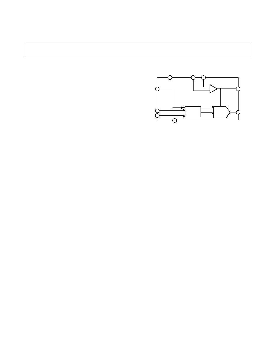
FUNCTIONAL BLOCK DIAGRAM
I
OUT
CLOCK
ADV7128
D0
D9
10
FS
ADJUST
10
V
AA
REFERENCE
AMPLIFIER
COMP
DAC
DATA
REGISTER
GND
V
REF
PRODUCT HIGHLIGHTS
1. Fast video refresh rate, 80 MHz.
2. Guaranteed monotonic to 10 bits. Ten bits of resolution al-
lows for implementation of linearization functions such as
gamma correction and contrast enhancement.
3. Compatible with a wide variety of high resolution color
graphics systems including RS-343A/RS-170 and the pro-
posed SMPTE 240M standard for HDTV.
4. Combined with a numerically controlled oscillator (AD9955),
it forms a complete frequency synthesizer (DDS).
5. Using the parts reduced power output DAC modes, it is
ideal for power and cost sensitive communications type
applications.
GENERAL DESCRIPTION
The ADV7128 (ADV
®
) is a video speed, digital-to-analog con-
verter on a single monolithic chip. It consists of a high speed,
10-bit, video D/A converters; a standard TTL input interface;
and a high impedance, analog output, current source.
The ADV7128 has a 10-bit pixel input port. A single +5 V
power supply, an external 1.23 V reference and pixel clock input
are and all that are required to make the part operational.
The ADV7128 is capable of generating video output signals
which are compatible with RS-343A, RS-170 and most pro-
posed production system HDTV video standards, including
SMPTE 240M.
The ADV7128 is fabricated in a +5 V CMOS process. Its
monolithic CMOS construction ensures greater functionality
with low power dissipation. The ADV7128 is available in a 28-
lead small outline IC (SOIC).
ADV is a registered trademark of Analog Devices, Inc.
FEATURES
80 MHz Pipelined Operation
10-Bit D/A Converters
RS-343A/RS-170 Compatible Outputs
TTL Compatible Inputs
+5 V CMOS Monolithic Construction
28-Pin SOIC Package
APPLICATIONS
High Definition Television (HDTV)
High Resolution Color Graphics
Digital Radio Modulation
CAE/CAD/CAM Applications
Image Processing
Instrumentation
Video Signal Reconstruction
Direct Digital Synthesis (DDS) & I/O Modulation
Wireless LAN
Wireless Local Loop
SPEED GRADES
80 MHz
50 MHz
30 MHz

REV. 0
2
ADV7128SPECIFICATIONS
(V
AA
= +5 V 5%; V
REF
= +1.235 V; R
L
= 37.5 , C
L
= 10 pF; R
SET
= 560
.
All specifications T
MIN
to T
MAX
1
unless otherwise noted.)
Parameter
K Version
Units
Test Conditions/Comments
STATIC PERFORMANCE
Resolution
10
Bits
Accuracy
Integral Nonlinearity, INL
±
1
LSB max
Differential Nonlinearity, DNL
±
1
LSB max
Guaranteed Monotonic
Gray Scale Error
±
5
% Gray Scale max
Max Gray Scale Current = (V
REF
* 7,969/R
SET
) mA
Coding
Binary
DIGITAL INPUTS
Input High Voltage, V
INH
2
V min
Input Low Voltage, V
INL
0.8
V max
Input Current, I
IN
±
1
µ
A max
V
IN
= 0.4 V or 2.4 V
Input Capacitance, C
IN
2
10
pF max
ANALOG OUTPUT
Gray Scale Current Range
15
mA min
22
mA max
Output Current
White Level
16.74
mA min
Typically 17.62 mA
18.50
mA max
Black Level
0
µ
A min
Typically 5
µ
A
50
µ
A max
LSB Size
17.28
µ
A typ
Output Compliance, V
OC
0
V min
+1.4
V max
Output Impedance, R
OUT
2
100
k
typ
Output Capacitance, C
OUT
2
30
pF max
I
OUT
= 0 mA
VOLTAGE REFERENCE
Voltage Reference Range, V
REF
1.14/1.26
V min/V max
V
REF
= 1.235 V for Specified Performance
Input Current, I
VREF
5
mA typ
POWER REQUIREMENTS
V
AA
5
V nom
I
AA
125
mA max
Typically 80 mA: 80 MHz Parts
100
mA max
Typically 70 mA: 50 MHz & 35 MHz Parts
Power Supply Rejection Ratio
2
0.5
%/% max
Typically 0.12%/%: f = 1 kHz, COMP = 0.1
µ
F
Power Dissipation
625
mW max
Typically 400 mW: 80 MHz Parts
500
mW max
Typically 350 mW: 50 MHz & 30 MHz Parts
DYNAMIC PERFORMANCE
Glitch Impulse
2, 3
50
pV secs typ
DAC Noise
2, 3, 4
200
pV secs typ
NOTES
1
Temperature range (T
MIN
to T
MAX
); 0
°
C to +70
°
C.
2
Sample tested at +25
°
C to ensure compliance.
3
TTL input values are 0 to 3 volts, with input rise/fall times
3 ns, measured between the 10% and 90% points. Timing reference points at 50% for inputs and
outputs. See timing notes in Figure 1.
4
This includes effects due to clock and data feedthrough.
Specifications subject to change without notice.
ADV7128
REV. 0
3
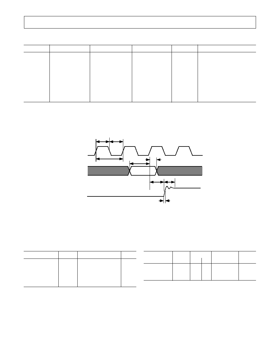
TIMING CHARACTERISTICS
1
(V
AA
= +5 V 5%; V
REF
= +1.235 V; R
L
= 37.5
, C
L
= 10 pF; R
SET
= 560
.
All specifications T
MIN
to T
MAX
2
unless otherwise noted.)
Parameter
80 MHz Version
50 MHz Version
30 MHz Version
Units
Conditions/Comments
f
MAX
80
50
30
MHz max
Clock Rate
t
1
3
6
8
ns min
Data & Control Setup Time
t
2
2
2
2
ns min
Data & Control Hold Time
t
3
12.5
20
33.3
ns min
Clock Cycle Time
t
4
4
7
9
ns min
Clock Pulse Width High Time
t
5
4
7
9
ns min
Clock Pulse Width Low Time
t
6
30
30
30
ns max
Analog Output Delay
20
20
20
ns typ
t
7
3
3
3
ns max
Analog Output Rise/Fall Time
t
8
3
12
15
15
ns typ
Analog Output Transition Time
NOTES
1
TTL input values are 0 to 3 volts, with input rise/fall times
3 ns, measured between the 10% and 90% points. Timing reference points at 50% for inputs
and outputs. See timing notes in Figure 1.
2
Temperature range (T
MIN
to T
MAX
): 0
°
C to +70
°
C
3
Sample tested at +25
°
C to ensure compliance.
Specifications subject to change without notice.
CLOCK
DATA
t
1
t
2
t
3
t
4
t
5
t
8
t
7
t
6
ANALOG OUTPUTS
(I
OUT
)
DIGITAL INPUTS
D0D9
NOTES
1. OUTPUT DELAY (
t
6
) MEASURED FROM THE 50% POINT OF THE RISING EDGE OF THE CLOCK TO THE 50%
POINT OF FULL-SCALE TRANSITION.
2. TRANSITION TIME (
t
8
) MEASURED FROM THE 50% POINT OF FULL-SCALE TRANSITION TO WITHIN 2% OF THE
FINAL OUTPUT VALUE.
3. OUTPUT RISE/FALL TIME (
t
7
) MEASURED BETWEEN THE 10% AND 90% POINTS OF FULL-SCALE TRANSITION.
Figure 1. Video Input/Output Timing
RECOMMENDED OPERATING CONDITIONS
Parameter
Symbol
Min
Typ
Max
Units
Power Supply
V
AA
4.75
5.00
5.25
Volts
Ambient Operating
Temperature
T
A
0
+70
°
C
Output Load
R
L
37.5
Reference Voltage
V
REF
1.14
1.235
1.26
Volts
ORDERING GUIDE
Accuracy
Temperature
Package
Model
Speed
DNL INL Range
Option*
ADV7128KR80 80 MHz
±
1
±
1
0
°
C to +70
°
C
R-28
ADV7128KR50 50 MHz
±
1
±
1
0
°
C to +70
°
C
R-28
ADV7128KR30 30 MHz
±
1
±
1
0
°
C to +70
°
C
R-28
*R = SOIC.
ADV7128
REV. 0
4
ABSOLUTE MAXIMUM RATINGS
*
V
AA
to GND . . . . . . . . . . . . . . . . . . . . . . . . . . . . . . . . . . .+7 V
Voltage on Any Digital Pin . . . . . . GND 0.5 V to V
AA
+0.5 V
Ambient Operating Temperature (T
A
) . . . . . . . . 0
°
C to +70
°
C
Storage Temperature (T
S
) . . . . . . . . . . . . . . . 65
°
C to +150
°
C
Junction Temperature (T
J
) . . . . . . . . . . . . . . . . . . . . . +150
°
C
Lead Temperature (Soldering, 10 secs) . . . . . . . . . . . . +300
°
C
Vapor Phase Soldering (2 minutes) . . . . . . . . . . . . . . . +220
°
C
I
OUT
to GND
1
. . . . . . . . . . . . . . . . . . . . . . . . . . . . . 0 V to V
AA
NOTES
*
Stresses above those listed under "Absolute Maximum Ratings" may cause
permanent damage to the device. This is a stress rating only and functional
operation of the device at these or any other conditions above those listed in the
operational sections of this specification is not implied. Exposure to absolute
maximum rating conditions for extended periods may affect device reliability.
1
Analog Output Short Circuit to any Power Supply or Common can be of an
indefinite duration.
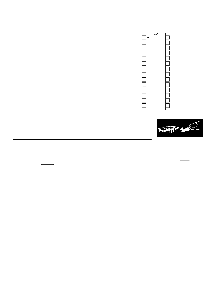
PIN CONFIGURATION
1
2
3
7
28
27
26
22
8
9
10
21
20
19
11
12
18
17
4
5
25
24
6
23
TOP VIEW
(Not to Scale)
13
14
16
15
ADV7128
D0
D1
D2
D3
D4
D5
D6
D7
D8
D9
R
SET
COMP
GND
GND
CLOCK
V
AA
I
OUT
V
AA
V
AA
V
AA
V
AA
V
AA
V
AA
V
AA
V
AA
V
AA
V
AA
V
REF
WARNING!
ESD SENSITIVE DEVICE
CAUTION
ESD (electrostatic discharge) sensitive device. Electrostatic charges as high as 4000 V readily
accumulate on the human body and test equipment and can discharge without detection.
Although the ADV7128 features proprietary ESD protection circuitry, permanent damage may
occur on devices subjected to high energy electrostatic discharges. Therefore, proper ESD
precautions are recommended to avoid performance degradation or loss of functionality.
PIN FUNCTION DESCRIPTION
Pin
Mnemonic
Function
CLOCK
Clock input (TTL compatible). The rising edge of CLOCK latches the R0R9, G0G9, B0B9, SYNC and
BLANK
pixel and control inputs. It is typically the pixel clock rate of the video system. CLOCK should be driven
by a dedicated TTL buffer.
D0D9
Data inputs (TTL compatible). Data is latched on the rising edge of CLOCK. D0 is the least significant data bit.
Unused data inputs should be connected to either the regular PCB power or ground plane.
I
OUT
Current output. This high impedance current source is capable of directly driving a doubly terminated 75
coaxial cable.
R
SET
Full-scale adjust control. A resistor (R
SET
) connected between this pin and GND, controls the magnitude of the
full-scale video signal. Note that the IRE relationships are maintained, regardless of the full-scale output current.
The relationship between R
SET
and the full-scale output current on I
OUT
is given by:
I
OUT
(mA) = 7,969 V
REF
(V)/R
SET
(
)
COMP
Compensation pin. This is a compensation pin for the internal reference amplifier. A 0.1
µ
F ceramic capacitor
must be connected between COMP and V
AA
.
V
REF
Voltage reference input. An external 1.23 V voltage reference must be connected to this pin. The use of an exter-
nal resistor divider network is not recommended. A 0.1
µ
F decoupling ceramic capacitor should be connected be-
tween V
REF
and V
AA
.
V
AA
Analog power supply (5 V
±
5%). All V
AA
pins on the ADV7128 must be connected.
GND
Ground. All GND pins must be connected.
ADV7128
REV. 0
5
TERMINOLOGY
Color Video (RGB)
This usually refers to the technique of combining the three pri-
mary colors of red, green and blue to produce color pictures
within the usual spectrum. In RGB monitors, three DACs are
required, one for each color.
Gray Scale
The discrete levels of video signal between reference black and
reference white levels. A 10-bit DAC contains 1024 different
levels, while an 8-bit DAC contains 256.
Raster Scan
The most basic method of sweeping a CRT one line at a time to
generate and display images.
Reference Black Level
The maximum negative polarity amplitude of the video signal.
Reference White Level
The maximum positive polarity amplitude of the video signal.
Video Signal
That portion of the composite video signal which varies in gray
scale levels between reference white and reference black. Also
referred to as the picture signal, this is the portion which may be
visually observed.
CIRCUIT DESCRIPTION AND OPERATION
The ADV7128 contains one 10-bit D/A converter, with one in-
put channel containing a 10-bit register. Also integrated on
board the part is a reference amplifier.
Digital Inputs
Ten bits of data (color information) D0D9 are latched into the
device on the rising edge of each clock cycle. This data is pre-
sented to the 10-bit DAC and is then converted to an analog
output waveform. See Figure 2.
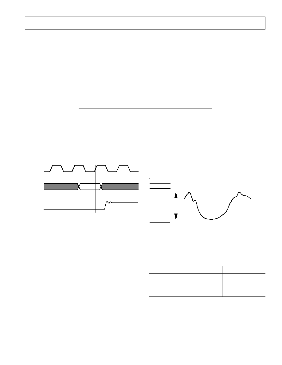
CLOCK
DATA
ANALOG
OUTPUTS
I
OUT
DIGITAL
INPUTS
D0D9
Figure 2. Video Data Input/Output
All these digital inputs are specified to accept TTL logic levels.
Clock Input
The CLOCK input of the ADV7128 is typically the pixel clock
rate of the system. It is also known as the dot rate. The dot rate,
and hence the required CLOCK frequency, will be determined
by the on-screen resolution, according to the following
equation:
Dot Rate = (Horiz Res)
×
(Vert Res)
×
(Refresh Rate)/
(Retrace Factor)
Horiz Res
=
Number of Pixels/Line.
Vert Res
=
Number of Lines/Frame.
Refresh Rate
=
Horizontal Scan Rate. This is the rate at
which the screen must be refreshed, typi-
cally 60 Hz for a noninterlaced system or
30 Hz for an interlaced system.
Retrace Factor =
Total Blank Time Factor. This takes into
account that the display is blanked for a
certain fraction of the total duration of
each frame (e.g., 0.8).
If we, therefore, have a graphics system with a 1024
×
1024
resolution, a noninterlaced 60 Hz refresh rate and a retrace fac-
tor of 0.8, then:
Dot Rate = 1024
×
1024
×
60/0.8
= 78.6 MHz
The required CLOCK frequency is thus 78.6 MHz.
All video data and control inputs are latched into the ADV7128
on the rising edge of CLOCK, as previously described in the
"Digital Inputs" section. It is recommended that the CLOCK
input to the ADV7128 be driven by a TTL buffer (e.g.,
74F244).
100
IRE
WHITE
LEVEL
BLACK
LEVEL
17.61 0.66
0 0
mA V
I
OUT
NOTES
1. OUTPUTS CONNECTED TO A DOUBLY TERMINATED 75
LOAD.
2. V
REF
= 1.235V, R
SET
= 560
.
3. RS343A LEVELS AND TOLERANCES ASSUMED ON ALL LEVELS.
Figure 3. I
OUT
Video Output Waveform
Table I. Video Output Truth Table for the ADV7128
Description
I
OUT
1
DAC Input Data
WHITE LEVEL
17.62
3FF
VIDEO
video
data
VIDEO to BLACK
video
data
BLACK LEVEL
0
00H
NOTE
1
Typical with full scale = 17.62 mA. V
REF
= 1.235 V, R
SET
= 560
.