 | ÐлекÑÑоннÑй компоненÑ: ADV7129 | СкаÑаÑÑ:  PDF PDF  ZIP ZIP |
Äîêóìåíòàöèÿ è îïèñàíèÿ www.docs.chipfind.ru
REV. 0
Information furnished by Analog Devices is believed to be accurate and
reliable. However, no responsibility is assumed by Analog Devices for its
use, nor for any infringements of patents or other rights of third parties
which may result from its use. No license is granted by implication or
otherwise under any patent or patent rights of Analog Devices.
a
192-Bit, 360 MHz True-Color
Video DAC with Onboard PLL
ADV7129
FEATURES
192-Bit Pixel Port Allows 2048 2048 24 Screen
Resolution
360 MHz, 24-Bit True-Color Operation
Triple 8-Bit D/A Converters
8:1 Multiplexing
Onboard PLL
RS-343A/RS-170 Compatible Analog Outputs
TTL Compatible Digital Inputs
Internal Voltage Reference
Standard 8-Bit MPU I/O Interface
DAC-DAC Matching: Typ 2%, Adjustable to 0.02%
+5 V CMOS Monolithic Construction
304-Pin PQFP Package
APPLICATIONS
Ultrahigh Resolution Color Graphics
Image Processing
Drives 24-Bit Color 2K 2K Monitors
GENERAL DESCRIPTION
The ADV7129 is a complete analog output, video DAC on a single
CMOS (ADV®) monolithic chip. The part is specifically designed
for use in the highest resolution graphics and imaging systems.
The ultimate level of integration, comprised of 360 MHz triple
8-bit DACs, a programmable pixel port, an internal voltage refer-
ence and an onboard PLL, makes the ADV7129 the only choice
for the very highest level of performance and functionality.
The device consists of three high speed, 8-bit, video D/A con-
verters (RGB). An onboard phase locked loop clock generator
is provided to provide high speed operation without requiring
high speed external crystal or clock circuitry.
The part is fully controlled through the MPU port by the on-
board command registers. This MPU port may be updated at
any time without causing sparkle effects on the screen.
ADV is a registered trademark of Analog Devices, Inc.
(continued on page 10)
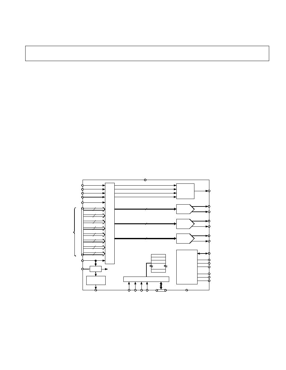
FUNCTIONAL BLOCK DIAGRAM
ODD/
EVEN
PIXEL
DATA
(RED,
GREEN,
BLUE)
B
C
D
E
F
G
A
H
LOADIN
LOADOUT
LPF
V
REF
IOR
MPU PORT
D7D0
CE R/
W
C0 C1
ADV7129
V
AA
GND
CONTROL
REGISTERS
IOR
IOG
IOG
IOB
IOB
RCOMP
GCOMP
BCOMP
R
RSET
R
GSET
R
BSET
BLANK
HSYNC
VSYNC
CSYNC
VOLTAGE
REFERENCE
SENSE/
SYNCOUT
8
CLOCK
CONTROL
PLL
INT PIXEL
CLOCK
24
24
24
24
24
24
24
24
BLANK
AND SYNC
LOGIC
8
GREEN
DAC
8
BLUE
DAC
8
RED
DAC
MUX
8:1
One Technology Way, P.O. Box 9106, Norwood, MA 02062-9106, U.S.A.
Tel: 617/329-4700
World Wide Web Site: http://www.analog.com
Fax: 617/326-8703
© Analog Devices, Inc., 1996
ADV is a registered trademark of Analog Devices, Inc..

ADV7129SPECIFICATIONS
All Versions
Conditions
1
Min
Typ
Max
Units
STATIC PERFORMANCE
3
Resolution (Each DAC)
8
Bits
Accuracy (Each DAC)
Integral Nonlinearity
±
1
LSB
Differential Nonlinearity
Guaranteed Monotonic
±
1
LSB
Gray Scale Error
±
5
% Gray Scale
Binary Coding
DIGITAL INPUTS
Input High Voltage, V
INH
2.0
V
AA
+ 0.5
V
Input Low Voltage, V
INL
GND 0.5
0.8
V
Input Current, I
IN
V
IN
= 0.4 V or 2.4 V
±
10
µ
A
Input Capacitance, C
IN
10
pF
DIGITAL OUTPUTS
Output High Voltage, V
OH
I
OH
= 400
µ
A
2.4
V
Output Low Voltage, V
OL
I
OL
= 3.2 mA
0.4
V
Floating-State Leakage Current
±
10
µ
A
Floating-State Output Capacitance
10
pF
ANALOG OUTPUTS
Gray Scale Current Range
10
60
mA
Output Current
White Level Relative to Black
50.16
52.80
55.44
mA
Black Level Relative to Blank
4.1
4.32
4.54
mA
Blank Level, Sync Disabled
0
5
50
µ
A
LSB Size
223
µ
A
DAC to DAC Matching
2
5
%
Output Compliance, V
OC
0
1.4
V
Output Impedance, R
OUT
10
k
Output Capacitance, C
OUT
20
pF
VOLTAGE REFERENCE
Voltage Reference Range, V
REF
V
REF
= 1.234 V for Specified
1.14
1.235
1.30
V
Input Current, I
VREF
Performance
5
µ
A
POWER REQUIREMENTS
V
AA
5
V
I
AA
4
Analog Current
160
200
mA
I
AA
4
Digital Current @ 360 MHz
360
400
mA
Power Supply Rejection Ratio
0.12
%/%
DYNAMIC PERFORMANCE
Clock and Data Feedthrough
5
30
dB
Glitch Impulse
50
pV secs
DAC to DAC Crosstalk
6
23
dB
NOTES
1
±
5% for all versions.
2
Temperature range (T
MIN
to T
MAX
), 0
°
C to +70
°
C, TJ (Silicon Junction Temperature)
100
o
C.
3
Static performance is measured with the Gain Error Registers set to 00H (disabled).
4
I
AA
is measured with a typical dynamic pattern, satisfying the absolute maximum current spec for the DACs.
5
Clock and Data Feedthrough is a function of the amount of overshoot and undershoot on the digital inputs. Glitch impulse includes clock and data
feedthrough. TTL input values are 0 V to 3 V, with input rise/fall times
3 ns, measured at the 10% and 90% points. Timing reference points are at 50% for
inputs and outputs.
6
DAC to DAC crosstalk is measured by holding one DAC high while the other two DACs are making low to high and high to low transitions.
Specifications subject to change without notice.
(V
AA
1
= +5 V, V
REF
= +1.235 V, R
RSET
, R
GSET,
R
BSET
= 280 , R
L
= 25
, C
L
= 10 pF.
All specifications T
MIN
to T
MAX
2
unless otherwise noted.)
REV. 0
2
ADV7129
3
REV. 0
TIMING SPECIFICATIONS
Parameter
Conditions
Min
Typ
Max
Units
CLOCK CONTROL & PIXEL PORT
4
LOADIN Clocking Rate, f
LCLK
10
45
MHz
LOADIN Cycle Time, t
1
16.67
ns
LOADIN Low Time, t
2
6.67
ns
LOADIN High Time, t
3
6.67
ns
LOADIN to LOADOUT Delay, t
4
5
ns
Pixel Setup Time, t
5
1
0
ns
Pixel Hold Time, t
6
4
2
ns
MPU PORT
R/W, C0, C1 Setup Time, t
7
10
2.5
ns
R/W, C0, C1 Hold Time, t
8
10
0.5
ns
CE
Low Time, t
9
25
ns
CE
High Time, t
10
25
ns
CE
Asserted to Data-Bus Driven, t
11
2
5
ns
CE
Asserted to Data-Bus Valid, t
12
20
ns
CE
Negated to Data-Bus Invalid, t
13
1
ns
CE
Negated to Data-Bus Three Stated, t
14
15
ns
Write Data (D7D0) Setup Time, t
15
10
ns
Write Data (D7D0) Hold Time, t
16
10
ns
ANALOG OUTPUTS
5
Analog Output Delay, t
17
@ 360 MHz
5
ns
Analog Output Rise/Fall Time, t
18
0.8
ns
Analog Output Transition Time, t
19
25
ns
RGB Analog Output Skew, t
SK
1.5
ns
Pipeline Delay, t
PD
19
PCLKs
PLL PERFORMANCE
6
Jitter (1
)
(LOADIN = 45 MHz)
55
ps rms
NOTES
1
TTL inputs values are 0 V to 3 V with input rise/fall times
3 ns, measured between the 10% and 90% points. Timing reference points at 50% for inputs and out-
puts. Analog output load
10 pF. Databus (D7D0) loaded as shown in Figure 1. Digital output load for SENSE
30 pF.
2
±
5% for all versions.
3
Temperature range (T
MIN
to T
MAX
), 0
°
C to +70
°
C.
4
Pixel Port consists of the following inputs: Pixel Inputs: RED [A-H], BLUE [A-H], GREEN [A-H].
5
Output Delay is measured from the 50% rising edge of LOADIN to the 50% point of full-scale transition on the A pixel. t
17
includes the analog delay due to DACs
and internal gate transitions plus the pipeline stages delay. The output delay for pixels B-H will be the output delay to the A pixel (t
17
) plus the appropriate number
of clock cycles. Output rise/fall time is measured between the 10% and 90% points of full-scale transition. Settling time is measured from the 50% point of full-scale
transition to the output remaining within 1%. (Settling Time does not include clock and data feedthrough.)
6
Jitter is measured by triggering on the output clock, delayed by 15
µ
s and then measuring the time period from the trigger edge to the next edge of the output clock
after the delay. This measurement is repeated multiple times and the rms value is determined.
Specifications subject to change without notice.
(V
AA
2
= +5 V, V
REF
= +1.235 V, R
RSET
, R
GSET,
R
BSET
= 280 , R
L
= 25 for IOG, IOR, IOB, C
L
= 10 pF.
All specifications T
MIN
to T
MAX
3
unless otherwise noted.)
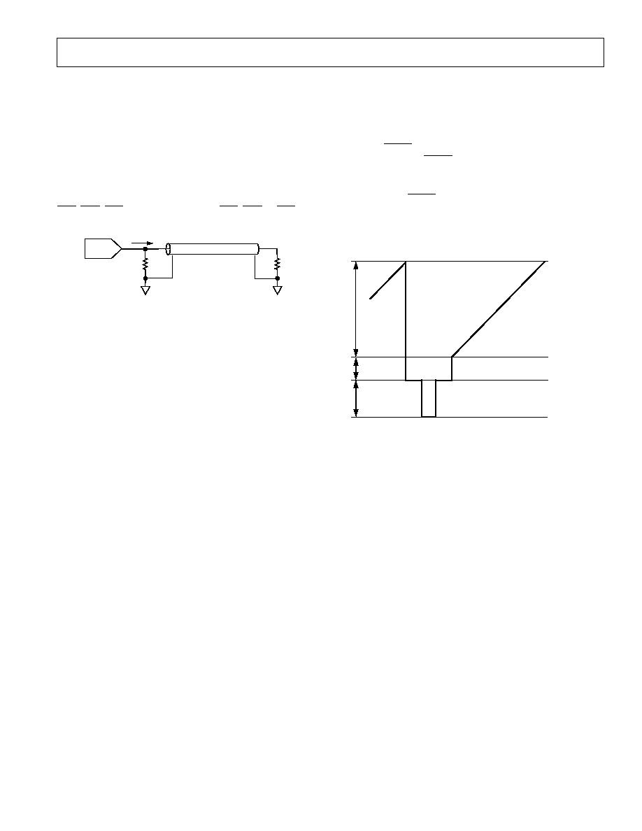
TO OUTPUT PIN
+2.1V
100pF
I
SINK
I
SOURCE
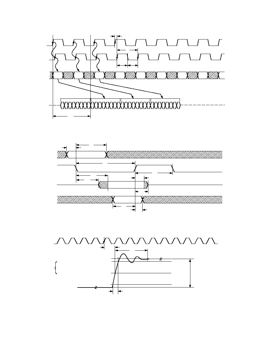
Figure 1. LOADIN vs. Pixel Input Data
ADV7129
4
REV. 0
A
N
...
H
N
A
N+1
...
H
N+1
A
N+2
...
H
N+2
DIGITAL INPUT TO ANALOG
OUTPUT PIPELINE
A
N+2
... H
N+2
A
N+1
... H
N+1
A
N
... H
N
A
N1
... H
N1
LOADOUT
LOADIN
PIXEL
INPUT
DATA
ANALOG
OUTPUT
DATA
t
2
t
3
t
4
t
1
t
PD
Figure 2. LOADIN vs. Pixel Input Data
R/
W
, C0, C1
CE
t
7
VALID
CONTROL DATA
t
13
t
16
D7D0
(READ MODE)
D7D0
(WRITE MODE)
R/
W
= 0
R/
W
= 1
t
8
t
9
t
12
t
11
t
10
t
14
t
15
Figure 3. Microprocessor Port (MPU) Interface Timing
PCLK
t
17
ANALOG
OUTPUTS
IOR
IOG
IOB
SYNCOUT
t
18
10 %
50 %
90 %
NOTE:
THIS DIAGRAM IS NOT TO SCALE.
FOR THE PURPOSES OF CLARITY, THE ANALOG OUTPUT WAVEFORM IS MAGNIFIED IN TIME AND AMPLITUDE W.R.T THE CLOCK WAVEFORM.
t
17
IS THE ONLY RELEVENT TIMING SPECIFICATION FOR
SYNCOUT
.
SYNCOUT
IS A DIGITAL VIDEO OUTPUT SIGNAL.
FULL-SCALE
TRANSITION
WHITE LEVEL
BLACK LEVEL
t
19
Figure 4. Analog Output Response vs. LOADIN
ADV7129
5
REV. 0
ABSOLUTE MAXIMUM RATINGS
1
V
AA
to GND . . . . . . . . . . . . . . . . . . . . . . . . . . . . . . . . . . . . . 7 V
Voltage on Any Digital Pin . . . . GND 0.5 V to V
AA
+ 0.5 V
Ambient Operating Temperature (T
A
) . . . . . . . . 0
°
C to +70
°
C
Storage Temperature (T
S
) . . . . . . . . . . . . . . 65
°
C to +150
°
C
Junction Temperature (T
J
) . . . . . . . . . . . . . . . . . . . . . +150
°
C
Lead Temperature (Soldering, 10 sec) . . . . . . . . . . . . . +260
°
C
Vapor Phase Soldering (1 minute) . . . . . . . . . . . . . . . . +220
°
C
Analog Outputs to GND
2
. . . . . . . . . . . GND 0.5 V to V
AA
Current on Any DAC Output . . . . . . . . . . . . . . . . . . . . 60 mA
NOTES
1
Stresses above those listed under "Absolute Maximum Ratings" may cause
permanent damage to the device. This is a stress rating only and functional
operation of the device at these or any other conditions above those listed in the
operational sections of this specification is not implied. Exposure to absolute
maximum rating conditions for extended periods may affect device reliability.
2
Analog Output Short Circuit to any Power Supply or Common can be of an
indefinite duration.
ORDERING GUIDE*
Model
Temperature Range
Package Option
ADV7129KS
0
°
C to +70
°
C
S-304
*Due to the specialized nature and application of this part, it is not automati-
cally available to order. Please contact your local sales office for details.
304-LEAD PQFP PIN CONFIGURATION
77
152
PIN NO. 1 IDENTIFIER
1
304
76
153
228
229
ROW A
ROW B
ROW D
ADV7129
PQFP
TOP VIEW
(Not to Scale)
ROW C
WARNING!
ESD SENSITIVE DEVICE
CAUTION
ESD (electrostatic discharge) sensitive device. Electrostatic charges as high as 4000 V readily
accumulate on the human body and test equipment and can discharge without detection.
Although the ADV7129 features proprietary ESD protection circuitry, permanent damage may
occur on devices subjected to high energy electrostatic discharges. Therefore, proper ESD
precautions are recommended to avoid performance degradation or loss of functionality.

ADV7129
6
REV. 0
PIN ASSIGNMENTS
Pin No.
Mnemonic
Pin No.
Mnemonic
Pin No.
Mnemonic
Pin No.
Mnemonic
1
GND
41
G4
C
81
GND
121
B4
E
2
GND
42
G4
B
82
GND
122
B4
D
3
GND
43
G4
A
83
G1
A
123
B4
C
4
GND
44
V
AA
84
G0
H
124
B4
B
5
GND
45
GND
85
G0
G
125
B4
A
6
GND
46
V
AA
86
G0
F
126
B3
H
7
R0
E
47
GND
87
G0
E
127
B3
G
8
R0
D
48
G3
H
88
G0
D
128
B3
F
9
R0
C
49
G3
G
89
G0
C
129
B3
E
10
R0
B
50
G3
F
90
G0
B
130
B3
D
11
R0
A
51
G3
E
91
G0
A
131
B3
C
12
G7
H
52
G3
D
92
B7
H
132
B3
B
13
G7
G
53
G3
C
93
B7
G
133
B3
A
14
G7
F
54
G3
B
94
B7
F
134
B2
H
15
G7
E
55
G3
A
95
B7
E
135
B2
G
16
G7
D
56
G2
H
96
B7
D
136
B2
F
17
G7
C
57
G2
G
97
B7
C
137
B2
E
18
G7
B
58
G2
F
98
B7
B
138
B2
D
19
G7
A
59
G2
E
99
B7
A
139
B2
C
20
G6
H
60
G2
D
100
B6
H
140
B2
B
21
G6
G
61
G2
C
101
B6
G
141
B2
A
22
G6
F
62
G2
B
102
B6
F
142
B1
H
23
G6
E
63
G2
A
103
B6
E
143
B1
G
24
G6
D
64
G1
H
104
B6
D
144
B1
F
25
G6
C
65
G1
G
105
B6
C
145
B1
E
26
G6
B
66
G1
F
106
B6
B
146
B1
D
27
G6
A
67
G1
E
107
B6
A
147
GND
28
G5
H
68
G1
D
108
B5
H
148
GND
29
G5
G
69
G1
C
109
B5
G
149
GND
30
G5
F
70
G1
B
110
B5
F
150
GND
31
G5
E
71
GND
111
B5
E
151
GND
32
G5
D
72
GND
112
B5
D
152
GND
33
G5
C
73
GND
113
B5
C
153
GND
34
G5
B
74
GND
114
B5
B
154
GND
35
G5
A
75
GND
115
B5
A
155
GND
36
G4
H
76
GND
116
V
AA
156
GND
37
G4
G
77
GND
117
GND
157
GND
38
G4
F
78
GND
118
B4
H
158
GND
39
G4
E
79
GND
119
B4
G
159
B1
C
40
G4
D
80
GND
120
B4
F
160
B1
B
*No Connect.
ADV7129
7
REV. 0
Pin No.
Mnemonic
Pin No.
Mnemonic
Pin No.
Mnemonic
Pin No.
Mnemonic
161
B1
A
197
R
BIAS
233
GND
269
LOADOUT
162
B0
H
198
SENSE/SYNCOUT
234
GND
270
R4
B
163
B0
G
199
V
REF
235
R6
H
271
R4
A
164
B0
F
200
GND
236
R6
G
272
R3
H
165
B0
E
201
D0
237
R6
F
273
R3
G
166
B0
D
202
D1
238
R6
E
274
R3
F
167
B0
C
203
D2
239
R6
D
275
R3
E
168
B0
B
204
D3
240
R6
C
276
R3
D
169
B0
A
205
GND
241
R6
B
277
R3
C
170
BLANK
206
V
AA
242
R6
A
278
R3
B
171
HSYNC
207
D4
243
R5
H
279
R3
A
172
VSYNC
208
D5
244
R5
G
280
R2
H
173
ODD/EVEN
209
D6
245
R5
F
281
R2
G
174
NC*
210
D7
246
V
AA
282
R2
F
175
GND
211
CE
247
GND
283
R2
E
176
GND
212
R/W
248
V
AA
284
R2
D
177
IOB
213
C0
249
GND
285
R2
C
178
IOB
214
C1
250
R5
E
286
R2
B
179
R
BSET
215
R7
H
251
R5
D
287
R2
A
180
B
COMP
216
R7
G
252
R5
C
288
R1
H
181
V
AA
217
R7
F
253
R5
B
289
R1
G
182
V
AA
218
R7
E
254
R5
A
290
R1
F
183
B
BIAS
219
R7
D
255
R4
H
291
R1
E
184
IOG
220
R7
C
256
R4
G
292
R1
D
185
IOG
221
R7
B
257
R4
F
293
R1
C
186
R
GSET
222
R7
A
258
R4
E
294
R1
B
187
G
COMP
223
GND
259
R4
D
295
R1
A
188
V
AA
224
GND
260
R4
C
296
R0
H
189
V
AA
225
GND
261
GND
297
R0
G
190
G
BIAS
226
GND
262
GND
298
R0
F
191
IOR
227
GND
263
V
AA
299
GND
192
IOR
228
GND
264
LPF
300
GND
193
R
RSET
229
GND
265
GND
301
GND
194
R
COMP
230
GND
266
LOADIN
302
GND
195
V
AA
231
GND
267
GND
303
GND
196
V
AA
232
GND
268
CSYNC
304
GND
*No Connect.
ADV7129
8
REV. 0
PIN DESCRIPTION
Mnemonic
Function
R7R0[A . . . H]
Red Pixel Port Inputs (TTL Compatible Inputs). Eight sets of eight bits latched on the rising edge of
LOADIN.
G7G0[A . . . H]
Green Pixel Port Inputs (TTL Compatible Inputs). Eight sets of eight bits latched on the rising edge of
LOADIN.
B7B0[A . . . H]
Blue Pixel Port Inputs (TTL Compatible Inputs). Eight sets of eight bits latched on the rising edge of
LOADIN.
BLANK
Composite Blank (TTL Compatible Input). This video control signal drives the analog outputs to the blanking
level. When BLANK is at logic "0," the pixel inputs are ignored. Pedestal selection is controlled by Bit CR15
of Command Register 1. BLANK is latched on the rising edge of LOADIN.
ODD/EVEN
Odd/Even Field Input (TTL Compatible Input). This input indicates which field of the frame is being dis-
played. An even field is selected by setting ODD/EVEN to logical "0." An odd field is selected by setting
ODD/EVEN to logical "1." ODD/EVEN should be changed only during vertical blank.
HSYNC
Horizontal-Sync Input (TTL Compatible Input). This control signal is latched on the rising edge of LOADIN.
VSYNC
Vertical-Sync Input (TTL Compatible Input). This control signal is latched on the rising edge of LOADIN.
CSYNC
Composite-Sync Input (TTL Compatible Input). This video control signal drives the analog outputs to the
SYNC
level. It is only asserted during the blanking period and does not override any other control or data in-
put. CR14, CR13 or CR12 of Command Register 1 must be set together with CR11 or Command Register 1 to
decode SYNC onto the IOR/IOR, IOG/IOG or IOB/IOB analog outputs, otherwise the SYNC input is ignored.
CE
Chip Enable Input (TTL Compatible Input). This input must be set to logic "0" when writing or reading over
the data bus (D7D0). Internally, data is latched on the rising edge of CE.
R/W
Read/Write pin (TTL Compatible Input). This signal is latched on the falling edge of CE. A high level indi-
cates a read operation and a low level indicates a write operation.
C0, C1
Register select pins (TTL Compatible Inputs). These inputs select which MPU port register is selected for
writing or reading. Data is latched on the falling edge of CE.
D7D0
Data Bus (TTL Compatible Input/Output Bus). Data, including color palette values and device control infor-
mation is written to and read from the device over this 8-bit, bidirectional databus. Any unused bits of the
data bus should be terminated through a resistor to either the digital power plane (V
CC
) or GND.
LOADIN
Pixel Data Load Input (TTL Compatible Input). This input latches the multiplexed pixel data, including
BLANK
, HSYNC, VSYNC, CSYNC, and ODD/EVEN into the device. This rising edge of this signal is used
to latch in the video signal inputs. It is also used as a reference frequency to generate an 8
×
multiple pixel
clock using the fixed reference onboard PLL.
LOADOUT
Pixel Data Load Output (TTL Compatible Output). This digital output is PCLK/8. If the onboard phase lock
loop is used, it has the same phase as LOADIN.
LPF
Low-Pass Filter Pin. This pin stabilizes the internal PLL. The following network is recommended.
0.001µF
100
LPF
0.1µF
V
AA
Figure 5.
ADV7129
9
REV. 0
Mnemonic
Function
IOR, IOG, IOB
Red, Green & Blue Current Outputs (High Impedance Current Sources). These RGB video outputs are
specified to directly drive RS-343A and RS-170 video levels into doubly terminated 50
or 75
loads.
IOR
, IOG, IOB
Differential Red, Green & Blue Current Outputs (High Impedance Current Sources). These RGB video
outputs are specified to directly drive RS-343A and RS-170 video levels into doubly terminated 50
or
75
loads. If the complementary outputs are not required, then these outputs should be tied to GND.
R
COMP
Red Compensation pin. This pin should be bypassed to V
AA
with 0.01
µ
F capacitor.
G
COMP
Green Compensation pin. This pin should be bypassed to V
AA
with 0.01
µ
F capacitor.
B
COMP
Blue Compensation pin. This pin should be bypassed to V
AA
with 0.01
µ
F capacitor.
R
RSET,
R
GSET,
R
BSET
DAC Output Full-Scale Adjust Control (Analog Input): A resistor from this pin to ground sets the current
in the DACs. The current in the DACs is set according to the equations:
I
OUT
= 12,950
×
V
REF
/R
SET
(SYNC not encoded on the DAC Output)
I
OUT
= 18,137
×
V
REF
/R
SET
(SYNC encoded on the DAC Output)
To generate RS 343-A video levels on the DAC outputs, a resistor value of 280
is recommended for
doubly terminated 50
lines. Any combination of R
SET
value, DAC termination resistor and programming
of SYNC and pedestal are possible provided that the maximum DAC current and the DAC output compli-
ance specifications are adhered to.
For example, in a doubly terminated 50
system with no SYNC or pedestal encoded on the DAC outputs,
an R
SET
value of 280
gives a DAC full-scale output of 52.8 mA, i.e., a white-to-black value of 1.4 V.
This example would give a 6 dB reduction in noise and feedthrough on the DAC outputs (compared to a
0.7 V full-scale value), but may require a 0.5X splitter at the monitor.
R
BIAS
Red Bias node. This node should be decoupled to V
AA
with a 0.01
µ
F capacitor.
G
BIAS
Green Bias node. This node should be decoupled to V
AA
with a 0.01
µ
F capacitor.
B
BIAS
Blue Bias node. This node should be decoupled to V
AA
with a 0.01
µ
F capacitor.
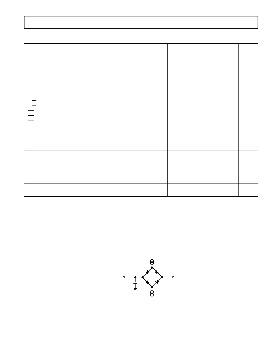
SENSE/SYNCOUT
Comparator Sense Output (TTL Compatible Output). This output will be logic "1" if one or more of the
analog outputs exceeds the internal voltage of the SENSE comparator circuit. It can be used to determine
the absence of a CRT monitor. The value of the SENSE Output corresponds to the current pixel at the out-
puts. The output can drive one CMOS load. This pin can alternately be programmed to be a TTL sync
output which is a delayed version of CSYNC.
V
REF
Voltage Reference (Analog Input/Output): This should always have a 0.1
µ
F decoupling capacitor attached
between V
REF
and V
AA
. If nothing else is connected then the DACs are driven by the internal voltage refer-
ence. If it is required to use a more accurate reference, then this pin acts as an overdrive input. An external
1.235 V voltage reference such as the AD1580 or equivalent is recommended to drive this input. (Note: It is
not recommended to use a resistor network to generate the voltage reference.)
V
AA
Power Supply (+5 V
±
5%). The part contains multiple power supply pins, all should be connected together
to one common +5 V filtered analog power supply.
GND
Analog Ground. The part contains multiple ground pins, all should be connected together to the system's
ground plane.

ADV7129
10
REV. 0
SENSE
If any one or more of the analog outputs, IOG, IOR and IOB,
exceed the internal voltage reference level (due to absence of
CRT), SENSE is set to logic "1." The SENSE output can drive
one CMOS load and can be used to determine the absence of a
CRT monitor.
CLOCK CONTROL CIRCUIT
The ADV7129 has an integrated clock control circuit. This cir-
cuit is capable of generating the internal clocking signals.
A lower frequency external clock generator is used by enabling
the onboard PLL. This fixed multiple PLL is used to speed up
LOADIN by a factor of 8. This onboard 8
×
clock multiplier is
activated by setting Bit CR20 of Command Register 2 from
logic "0" to logic "1." It must be set up after power-up.
MICROPROCESSOR (MPU) PORT
The ADV7129 supports a standard MPU interface. All the
functions of the part are controlled via this MPU port. Direct
access is gained to the address register and all the control regis-
ters as well as the cursor palette. The following sections de-
scribe the setup for reading and writing to all of the devices'
registers.
MPU Interface
The MPU interface consists of a bidirectional, 8-bit wide data-
bus and interface control signals R/W, CE, C1, C0. Two write
operations are required to set up the lower 8 bits and higher
2 bits of the Address Register.
Register Mapping
The ADV7129 contains a number of onboard registers includ-
ing the Address Register, Command Registers and Gain Error
Registers. Control Lines C1-C0 determine whether the Address
Register is being pointed to (upper or lower bytes) or whether
the other registers are being accessed.
The R/W and CE control inputs allow read and write access.
All registers can to read and written to.
Power-On Reset
After power-up, the ADV7129 must be set to perform a reset
operation. This is achieved by resetting the PLL (a low to high
transition on Bit CR20 of Command Register 2). This initial-
izes the pixel port such that the pixel sequence ABCDEFGH
starts at A. This reset can be performed as the registers are be-
ing initialized. The Command Registers power up in an indeter-
minate state and must be set up for the required operation. The
power-on is activated when V
AA
goes from 0 V to 5 V. This is
active for 1
µ
s. The ADV7129 should not be accessed during
this period.
Register Accesses
The MPU can write to or read from all of the ADV7129s' regis-
ters. Figure 6 shows the Control Registers and C1-C0 Control
Input Truth Table. The read/write timing is controlled by the
CE
and R/W inputs. The Address Register determines which
Control Register is being accessed.
The registers can be addressed directly by two write cycles to set
up the high and low bytes of Address Register and then by a
read or write cycle of the MPU.
(continued from page 1)
The ADV7129 supports 24-bit true-color formats where screen
resolution is the primary design goal. The individual Red,
Green and Blue pixel input ports allow true-color image rendi-
tion at resolutions of 2048
×
2048
×
24 bit.
The ADV7129 is capable of generating RGB video output sig-
nals that are compatible with RS-343A and RS-170 video stan-
dards, without requiring external buffering.
An internal voltage reference is also provided to simplify system
design.
The ADV7129 is fabricated in a +5 V CMOS process.
The ADV7129 is packaged in a 304-pin PQFP package.
CIRCUIT DETAILS AND OPERATION
Digital video or pixel data is latched into the ADV7129 over the
pixel port. The data is multiplexed and latched into the three 8-
bit digital-to-analog converters (DACs) and output as an RGB
video signal.
The ADV7129 can be broken into three sections for purposes of
clarity of explanation:
1. Pixel port and clock control circuit.
2. MPU port, registers and cursor.
3. Digital-to-analog converters and video outputs.
Pixel Port and Clock Circuits
The pixel port of the ADV7129 is directly interfaced to the
video/graphics pipeline of a computer graphics subsystem. It is
connected directly through a gate array to the video RAM of the
system's frame buffer. The pixel port of the ADV7129 consists of:
Color Data:
RED, GREEN, BLUE
Pixel Controls:
HSYNC
, VSYNC, CSYNC, BLANK
The associated clocking signals for the pixel port include:
Clock Input
LOADIN
Clock Output
LOADOUT
Pixel Port (Color Data)
The ADV7129 has 192 color data inputs. This supports 24-bit
true color with 8:1 multiplexing.
Color data is always latched on the rising edge of LOADIN.
LOADOUT is generated internally by the ADV7129. The fre-
quency of LOADOUT is the internal clock frequency (PCLK)
divided by 8.
Other pixel data signals latched into the part by LOADIN in-
clude HSYNC, BLANK, VSYNC and CSYNC.
HSYNC
, VSYNC, CSYNC, BLANK
The BLANK and SYNC video control signals drive the analog
outputs to the blanking and sync levels respectively. These are
latched on the rising edge of LOADIN. The SYNC information
can be encoded onto any of the IOG, IOR or IOB analog out-
puts by setting Bits CR12, CR13 or CR14 of Command Regis-
ter 1 to logic "1."
The SYNC information is ignored if Bits CR12, CR13 and
CR14 of Command Register 1 are set to logic "0."
The SYNC and BLANK information can be decoded onto the
inverted outputs by setting CR10 and CR11 of Command
Register 1 to logic level "1."
ADV7129
11
REV. 0
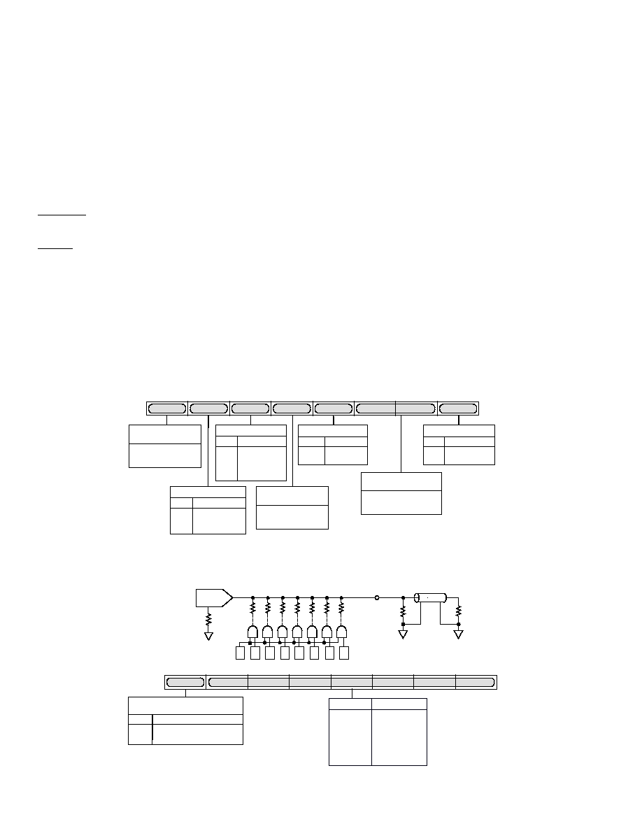
REGISTER PROGRAMMING
The following section describes each register, including Address
Register and each of the Control Registers in terms of its
configuration.
Address Register (A10A0)
As illustrated previously, the C1C0 inputs, in conjunction with
the Address Register specify which control register, or palette
RAM location is accessed by the MPU port. The Address Reg-
ister is 16 bits wide and can be read from as well as written to.
CONTROL REGISTERS
A large bank of registers can be accessed using the Address reg-
ister and C1C0. Access is made first by writing the Address
Register with the appropriate address to point to the particular
Control Register, and then performing an MPU access to the
Control Register.
ADDRESS REGISTER
(A10A0)
(A10A0)
REGISTER ACCESS
4FF412
RESERVED
411
COMMAND REGISTER 2
410 RESERVED
40F
RESERVED
40E
RESERVED
40D
RESERVED
40C
RESERVED
40B
RESERVED
40A
RESERVED
409
RESERVED
408
RESERVED
407
BLUE DAC GAIN ERROR REGISTER
406
GREEN DAC GAIN ERROR REGISTER
405
RED DAC GAIN ERROR REGISTER
004 RESERVED
403
RESERVED
402
RESERVED
401 RESERVED
400
COMMAND REGISTER 1
0003FF
RESERVED
C1
C0
R/
W
0
0
0
WRITE TO ADDRESS REGISTER (LOWER BYTE)
0
1
0
WRITE TO ADDRESS REGISTER (UPPER BYTE)
1
0
0
WRITE TO REGISTERS
0
0
1
READ FROM ADDRESS REGISTER (LOWER BYTE)
0
1
1
READ FROM ADDRESS REGISTER (UPPER BYTE)
1
0
1
READ FROM REGISTERS
1
1
X
RESERVED
Figure 6. Control Registers
COMMAND REGISTER 1 (CR1)
(Address Register (A10A0) = 400H)
This register contains a number of control bits as shown in the
diagram. CR1 is an 8-bit wide register.
Figure 7 shows the various operations under the control of CR1.
This register can be read from as well as written to. Bit CR16 is
reserved and should be set to logic "1."
COMMAND REGISTER 1-BIT DESCRIPTION
BLANK
Control on Inverted Outputs (CR10):
This bit specifies whether the video BLANK is to be decoded
onto the inverted analog outputs or ignored.
SYNC
Control on Inverted Outputs (CR11)
This bit specifies whether the video SYNC is to be decoded
onto the inverted analog outputs or ignored.
SYNC
Recognition on Blue (CR12)
This bit specifies whether the video SYNC input is to be de-
coded onto the IOB analog output or ignored.
SYNC
Recognition on Green (CR13)
This bit specifies whether the video SYNC input is to be de-
coded onto the IOG analog output or ignored.
SYNC
Recognition on Red (CR14)
This bit specifies whether the video SYNC input is to be de-
coded onto the IOR analog output or ignored.
Pedestal Enable Control (CR15)
This bit specifies whether a 0 IRE or a 7.5 IRE blanking pedes-
tal is to be generated on the video outputs.
Display Mode Control (CR17)
This bit controls whether the display is interlaced or noninterlaced.
CR17
CR16
CR15
CR14
CR13
CR12
CR11
CR10
CR16 = 0
(RESERVED)
ZERO MUST BE
WRITTEN TO THIS BIT
INTERLACE ENABLE
0
DISABLE
1
ENABLE
CR17
PEDESTAL ENABLE
CONTROL
0
0 IRE
1
7.5 IRE
CR15
SYNC RECOGNITION
CONTROL (IOG)
0
IGNORE
1
DECODE
CR13
SYNC RECOGNITION
CONTROL (IOB)
0
IGNORE
1
DECODE
CR12
SYNC RECOGNITION
CONTROL (IOR)
0
IGNORE
1
DECODE
CR14
PEDESTAL CONTROL
(
IOR
,
IOG
,
IOB
)
0
DISABLE BLANK ON
INVERTED OUTPUTS
1
DECODE BLANK ON
INVERTED OUTPUTS
CR10
SYNC CONTROL
(
IOR
,
IOG
,
IOB
)
0
DISABLE SYNC ON
INVERTED OUTPUTS
1
DECODE SYNC ON
INVERTED OUTPUTS
CR11
Figure 7. Command Register 1
ADV7129
12
REV. 0
COMMAND REGISTER 2 (CR2)
(Address Register (A10A0) = 411H)
This register contains a number of control bits as shown in the
diagram. CR2 is an 8-bit wide register. CR27, CR24, CR22
and CR21 are reserved and should be set to logic "0." Figure 8
shows the various operations under the control of CR2. This
register can be read from as well as written to.
COMMAND REGISTER 2-BIT DESCRIPTION
PLL Control (CR20)
This bit resets the PLL divider when set to logic "0" and re-
leases it when set to logic "1."
SYNCOUT
Control (CR23)
This bit is an enable for SYNCOUT. If this bit is set to logic
"1," the SENSE output becomes a pipelined version of
CSYNC
. Otherwise the SENSE output remains unaffected.
SENSE Bit (CR25)
This output bit is used to determine the absence of a CRT
monitor. When CR25 is set to logic "1," a CRT is not present.
With some diagnostic code, the presence of loading on the indi-
vidual RGB lines can be determined. The reference is generated
by a voltage divider from the external voltage reference on the
V
REF
pin. For the proper operation, the following levels should
be applied to the comparator by the IOR, IOG and IOB outputs:
DAC Low Voltage
250 mV.
DAC High Voltage
450 mV.
VCO Override Bit (CR26)
This bit is used to override the VCO and set the PLL to the
lowest frequency possible. If the external LOADIN source takes
some time before it reaches its required frequency, the internal
PLL can become unstable as it tries to track to a varying
LOADIN signal. The VCO override bit can be set to logic level
"0" and then released (set to logic level "1") to allow the VCO
to track to the input after it has stabilized. It is required to allow
200
µ
s before the VCO override bit is released.
GAIN ERROR REGISTERS
(Address Register (A10A0) = 405H407H)
The Red, Green and Blue Gain Error Registers allow the user to
compensate for any channel-to-channel variations in the video
output system. They control internal resistors from each of the
three DAC outputs to GND, i.e., they appear in parallel with
the external termination resistor across the DAC outputs. This
allows the RGB output voltages to be adjusted as the value of
R
INT
is varied. A logic "1" on any of the control bits GR06 to
GR00 switches in the appropriate resistor. A logic "0" disables
or open circuits the resistor. Bit GR07 of the Gain Error
Register enables or disables the Gain Error Adjust. Figure 9
shows the typical resistor values for these internal resistances
versus R
SET
.
CR27
CR26
CR25
CR24
CR23
CR22
CR21
CR20
SENSE OUTPUT
0
MONITOR
PRESENT
1
MONITOR
NOT PRESENT
CR25
SYNCOUT CONTROL
0
IGNORE
1
DECODE
CR23
RESERVED
(CR27)
THIS BIT SHOULD BE
SET TO LOGIC "0"
VCO OVERRIDE
0
VCO OVERRIDE
1
NORMAL PLL
OPERATION
CR26
RESERVED
(CR24)
THIS BIT SHOULD BE
SET TO LOGIC "0"
RESERVED
(CR22, CR21)
THESE BITS SHOULD BE
SET TO LOGIC "0"
PLL RESET
0
RESET PLL
1
RELEASE PLL
CR20
Figure 8. Command Register 2
x
x
x
x
x
x
x
1
GAIN ERROR REGISTER
R
SET
DACs
R
6
R
5
R
4
R
3
R
2
R
1
R
0
INTERNAL RESISTORS
I
OUT
PIN
R
T1
R
T2
GR06 R6
GR05 R5
GR04 R4
GR03 R3
GR02 R2
GR01 R1
GR00 R0
47
923
1926
3476
6979
16610
27037
REGISTER
(RESET = 280
)
(CABLE)
(MONITOR)
GR07
GR06
GR05
GR04
GR03
GR02
GR01
GR00
GAIN ERROR
CONTROL
0 DISABLE GAIN ERROR ADJ
1
ENABLE GAIN ERROR ADJ
GR07
Figure 9. Gain Error Register
ADV7129
13
REV. 0
DIGITAL-TO-ANALOG CONVERTERS (DACS)
AND VIDEO OUTPUTS
The ADV7129 contains three high speed video DACs. The
DAC outputs are represented as the three primary analog color
signals IOR (red video), IOG (green video) and IOB (blue
video).
DACs and Analog Outputs
The part contains three matched 8-bit digital-to-analog converters.
The DACs are designed using an advanced, high speed, seg-
mented architecture. The bit currents corresponding to each
digital input are routed to either IOR, IOG, IOB (bit = "1") or
IOR
, IOG, IOB (bit = "0"). Normally IOR, IOG, & IOB are
connected to GND.
Z
O
= 50
(CABLE)
Z
L
= 50
(MONITOR)
IOR, IOG, IOB
DACs
Z
S
= 50
(SOURCE TERMINATION)
Figure 10. DAC Output Termination (Doubly Terminated
50
Load)
The analog video outputs are high impedance current sources.
Each of the these three RGB current outputs are specified to di-
rectly drive a 25
load (doubly-terminated 50
).
Reference Input and R
SET
An external 1.235 V voltage reference is preferred to set up the
analog outputs of the ADV7129. The reference voltage is con-
nected to the V
REF
input. In the absence of an external refer-
ence, the on-chip voltage reference is internally connected to
the V
REF
pin. The internal reference will set up the DAC cur-
rents, although with slightly less accuracy.
A resistor R
SET
is connected between the R
SET
(R
RSET
, R
GSET
,
R
BSET
) input of the part and ground. An R
SET
value of 280
corresponds to the generation of two times RS-343A video lev-
els into a doubly-terminated 50
load. Figure 11 illustrates the
resulting video waveform and the Video Output Truth Table il-
lustrates the corresponding control input stimuli. On the
ADV7129 SYNC can be encoded on any of the analog signals,
however in practice, SYNC is generally encoded on either the
IOG output or on all of the video outputs.
Any combination of R
SET
, DAC termination resistors and
programming of SYNC and pedestal are possible provided that
the maximum DAC current of 60 mA and the DAC output
compliance specifications are adhered to. The following tables
show the current levels for different values of R
SET
resistors and
R
LOAD
termination.
GRAY SCALE
7.5 IRE
92.5 IRE
40 IRE
SYNC LEVEL
BLANK LEVEL
BLACK LEVEL
WHITE LEVEL
Figure 11. Composite Video Waveform SYNC Decoded;
Pedestal = 7.5 IRE
ADV7129
14
REV. 0
Table I. Video Output Truth Table (R
SET
= 398
, R
LOAD
= 37.5
)
O/P with Sync
O/P with Sync
DAC
Description
Enabled (mA)
Disabled (mA)
SYNC
BLANK
Input Data
WHITE LEVEL
26.67
19.05
1
1
FFH
VIDEO
Video + 9.05
Video + 1.44
1
1
Data
VIDEO to BLANK
Video + 1.44
Video + 1.44
0
1
Data
BLACK LEVEL
9.05
1.44
1
1
00H
BLACK to BLANK
1.44
1.44
0
1
00H
BLANK LEVEL
7.62
0
1
0
xxH
SYNC
LEVEL
0
0
0
0
xxH
Table II. Video Output Truth Table (R
SET
= 560
, R
LOAD
= 25
)
O/P with Sync
O/P with Sync
DAC
Description
Enabled (mA)
Disabled (mA)
SYNC
BLANK
Input Data
WHITE LEVEL
40
28.57
1
1
FFH
VIDEO
Video + 13.6
Video + 2.14
1
1
Data
VIDEO to BLANK
Video + 2.16
Video + 2.14
0
1
Data
BLACK LEVEL
13.6
2.14
1
1
00H
BLACK to BLANK
2.14
2.14
0
1
00H
BLANK LEVEL
11.44
0
1
0
xxH
SYNC
LEVEL
0
0
0
0
xxH
Table III. Video Output Truth Table (R
SET
= 280
, R
LOAD
= 25
)
O/P with Sync
DAC
Description
Disabled (mA)
SYNC
BLANK
Input Data
WHITE LEVEL
52.8
0
0
FFH
VIDEO
Video + 0
0
0
Data
VIDEO to BLACK
Video + 0
0
0
Data
BLACK LEVEL
0
0
0
xxH

ADV7129
15
REV. 0
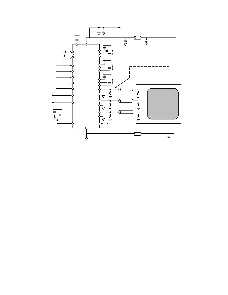
APPENDIX I
BOARD DESIGN AND LAYOUT CONSIDERATIONS
The ADV7129 is a highly integrated circuit containing both
precision analog and high speed digital circuitry. It has been
designed to minimize interference effects on the integrity of the
analog circuitry by the high speed digital circuitry. It is impera-
tive that these same design and layout techniques be applied to
the system level design such that high speed, accurate perfor-
mance is achieved. The "Recommended Analog Circuit Layout"
(see Figure 12) shows the analog interface between the device and
monitor.
The layout should be optimized for lowest noise on the ADV7129
power and ground lines by shielding the digital inputs and pro-
viding good decoupling. The lead length between groups of V
AA
and GND pins should by minimized so as to minimize inductive
ringing.
Ground Planes
The ground plane should encompass all ADV7129 ground pins,
voltage reference circuitry, power supply bypass circuitry for the
ADV7129, the analog output traces, and all the digital signal
traces leading up to the ADV7129. The analog ground plane
should be separated from the system ground plane by a ferrite
bead.
Power Planes
The ADV7129 and any associated analog circuitry should have its
own power plane, referred to as the analog power plane (V
AA
).
This power plane should be connected to the regular PCB power
plane (V
CC
) at a single point through a ferrite bead. This bead
should be located within three inches of the ADV7129.
The PCB power plane should provide power to all digital logic
on the PC board, and the analog power plane should provide
power to all ADV7129 power pins and voltage reference circuitry.
Plane-to-plane noise coupling can be reduced by ensuring that
portions of the regular PCB power and ground planes do not
overlay portions of the analog power plane, unless they can be
arranged such that the plane-to-plane noise is common mode.
Supply Decoupling
For optimum performance, bypass capacitors should be installed
using the shortest leads possible, consistent with reliable opera-
tion, to reduce the lead inductance. Best performance is obtained
with 0.1
µ
F ceramic capacitor decoupling. Each group of V
AA
pins on the ADV7129 must have at least one 0.1
µ
F decoupling
capacitor to GND. These capacitors should be placed as close
as possible to the device.
It is important to note that while the ADV7129 contains cir-
cuitry to reject power supply noise, this rejection decreases with
frequency. If a high frequency switching power supply is used,
the designer should pay close attention to reducing power
supply noise and consider using a three terminal voltage
regulator for supplying power to the analog power plane.
Digital Signal Interconnect
The digital inputs to the ADV7129 should be isolated as
much as possible from the analog outputs and other analog
circuitry. Also, these input signals should not overlay the
analog power plane.
Due to the high clock rates involved, long clock lines to the
ADV7129 should be avoided to reduce noise pickup.
Any active termination resistors for the digital inputs should
be connected to the regular PCB power plane (V
CC
), and
not the analog power plane.
Analog Signal Interconnect
The ADV7129 should be located as close as possible to the
output connectors to minimize noise pickup and reflections
due to impedance mismatch.
The video output signals should overlay the ground plane,
and not the analog power plane, to maximize the high fre-
quency power supply rejection.
Digital Inputs, especially Pixel Data Inputs and clocking
signals (LOADOUT, LOADIN, etc.) should never overlay
any of the analog signal circuitry and should be kept as far
away as possible.
For best performance, the analog outputs should each have
a 50
load resistor connected to GND. These resistors
should be placed as close as possible to the ADV7129 so as
to minimize reflections.
There are a number of precautions that the user can take to
minimize the effects of data feedthrough.
a. Apply external filtering to the DAC outputs.
b. Reduce input voltage risetime. From experiments, it has
been seen that a reduction from 2 ns to 4 ns gives signifi-
cant improvement.
c. Reduce input voltage swing. A reduction from 5 V to 3 V
gives significant improvement.
d. Use series resistors on the pixel inputs (e.g., 100
).
e. The part can be run at 2
×
DAC current levels as shown
in the DAC output. The differential outputs can then be
connected through a differential to single balun trans-
former to eliminate common-mode noise. A phase split-
ter should be used to reduce the 2
×
levels to 1
×
at the
monitor end.
ADV7129
16
REV. 0
PIXEL
DATA
192
R
BIAS
G
BIAS
B
BIAS
R
COMP
G
COMP
B
COMP
IOR
IOR
IOG
IOG
IOB
IOB
R
RSET
G
RSET
B
RSET
+5V(V
AA
)
ANALOG POWER PLANE
10µF
33µF
FERRITE BEAD
+5V
(BOARD SUPPLY V
CC
)
V
AA
EACH
0.01µF
V
AA
EACH
0.01µF
V
AA
EACH
280
50
50
V
AA
V
REF
V
AA
0.1µF
SENSE/
SYNCOUT
0.1µF
0.01µF
(REPEATED FOR EACH GROUP OF V
AA
PINS)
FERRITE BEAD
GND
ANALOG GROUND PLANE
DIGITAL GROUND
PLANE
BOARD GROUND
MONITOR (CRT)
ADV7129
0.01µF
0.1µF
V
AA
LPF
LOADOUT
LOADIN
CLOCK
(45MHz)
ODD/
EVEN
CSYNC
HSYNC
VSYNC
BLANK
AN OPTIONAL BALUN TRANSFORMER
CAN BE USED ON VIDEO AND
COMPLEMENTARY OUTPUTS FOR
IMPROVED PERFORMANCE
(DOESN'T SHOW MPU PORT FOR CLARITY)
50
50
50
50
100
Figure 12. Typical Connection Diagram
ADV7129
17
REV. 0
APPENDIX II
THERMAL AND ENVIRONMENTAL CONSIDERATIONS
The ADV7129 is a very highly integrated monolithic silicon
device. This high level of integration inevitably leads to consid-
eration of thermal and environmental conditions which the
ADV7129 must operate in. Reliability of the device is enhanced
by keeping it as cool as possible. In order to avoid destructive
damage to the device, the absolute maximum junction tempera-
ture must never be exceeded. Certain applications, depending
on ambient temperature and pixel data rates may require forced
air cooling or external heatsinks. The following data is intended as
a guide in evaluating the operating conditions of a particular appli-
cation so that optimum device and system performance is achieved.
It should be noted that information on package characteristics
published herein may not be the most up to date at the time of
reading this. Advances in package compounds and manufacture
will inevitably lead to improvements in the thermal data. Please
contact your local sales office for the most up-to-date information.
Package Characteristics
Junction-to-Case (
JC
) Thermal Resistance for this particular
part is:
JC
= 8.9
°
C/W
(Note:
JC
is independent of airflow.)
The maximum silicon junction temperature should be limited to
100
°
C. Temperatures greater than this will reduce long-term
device reliability. To ensure that the silicon junction tempera-
ture stays within prescribed limits, the addition of an external
heatsink can be used if the junction temperature is brought be-
yond the maximum limit.
Junction-to-Ambient (
JA
) Thermal Resistance for this particu-
lar part is:
JA
= 25.9
°
C/W (Still Air)
JA
= will significantly decrease in air flow.
Thermal Model
The junction temperature of the device in a specific application
is given by:
T
J
= T
A
+ P
D
(
JC
+
CA
)
(1)
or
T
J
= T
A
+ P
D
(
JA
)
(2)
where:
T
J
=
Junction Temperature of Silicon (
°
C)
T
A
=
Ambient Temperature (
°
C)
P
D
=
Power Dissipation (W)
JC
=
Junction to Case Thermal Resistance (
°
C/W)
CA
=
Case to Ambient Thermal Resistance (
°
C/W)
JA
=
Junction to Ambient Thermal Resistance (
°
C/W)
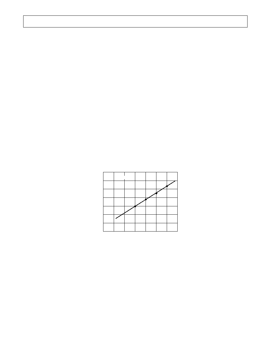
SPEED MHz
160
CURRENT mA
200
240
280
320
360
550
500
475
450
425
525
V
AA
= +5V
Figure 13. Supply Current vs. Frequency
ADV7129
18
REV. 0
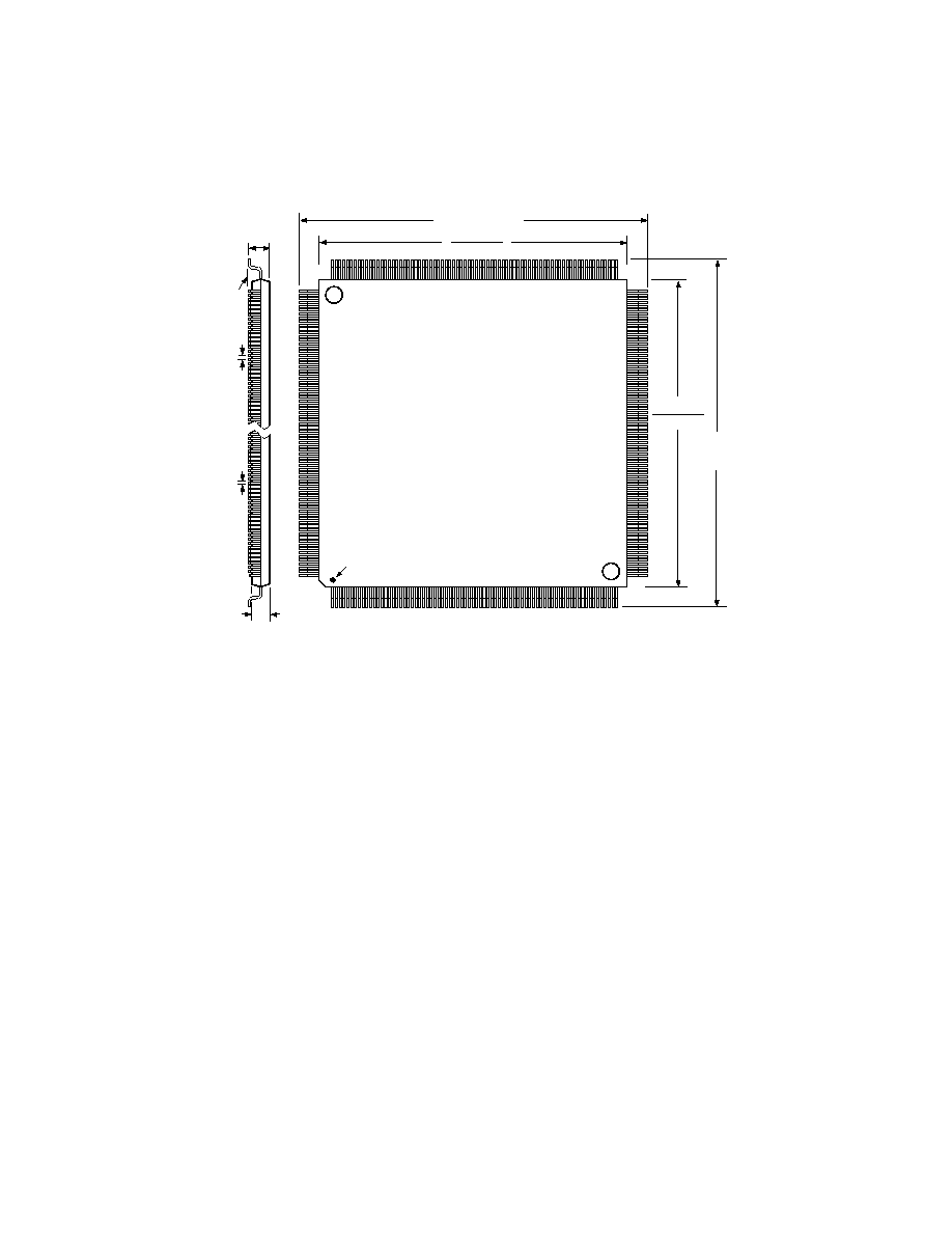
OUTLINE DIMENSIONS
Dimensions shown in inches and (mm).
304-Lead Plastic Quad Flatpack
(S-304)
SEATING
PLANE
0.167 (4.23)
NOM
0.150 (3.80) NOM
0.0197
(0.50)
NOM
0.008
(0.20)
NOM
1
229
228
153
304
77
76
TOP VIEW
(PINS DOWN)
PIN 1 IDENTIFIER
152
ROW A
ROW C
ROW B
ROW D
1.579 (40.10)
1.571 (39.90)
1.677 (42.60) NOM
1.579 (40.10)
1.571 (39.90)
1.677
(42.60)
NOM

19

PRINTED IN U.S.A.
C2215610/96
20