 | –≠–ª–µ–∫—Ç—Ä–æ–Ω–Ω—ã–π –∫–æ–º–ø–æ–Ω–µ–Ω—Ç: ADXL202J | –°–∫–∞—á–∞—Ç—å:  PDF PDF  ZIP ZIP |

REV. B
Information furnished by Analog Devices is believed to be accurate and
reliable. However, no responsibility is assumed by Analog Devices for its
use, nor for any infringements of patents or other rights of third parties
which may result from its use. No license is granted by implication or
otherwise under any patent or patent rights of Analog Devices.
a
Low Cost 2
g/ 10 g Dual Axis
i
MEM
S
Æ
Accelerometers
with Digital Output
ADXL202/ADXL210
FEATURES
2-Axis Acceleration Sensor on a Single IC Chip
Measures Static Acceleration as Well as Dynamic
Acceleration
Duty Cycle Output with User Adjustable Period
Low Power <0.6 mA
Faster Response than Electrolytic, Mercury or Thermal
Tilt Sensors
Bandwidth Adjustment with a Single Capacitor Per Axis
5 m
g Resolution at 60 Hz Bandwidth
+3 V to +5.25 V Single Supply Operation
1000
g Shock Survival
APPLICATIONS
2-Axis Tilt Sensing
Computer Peripherals
Inertial Navigation
Seismic Monitoring
Vehicle Security Systems
Battery Powered Motion Sensing
A
IN
2 =
One Technology Way, P.O. Box 9106, Norwood, MA 02062-9106, U.S.A.
Tel: 781/329-4700
World Wide Web Site: http://www.analog.com
Fax: 781/326-8703
© Analog Devices, Inc., 1999
FUNCTIONAL BLOCK DIAGRAM
DEMOD
R
FILT
32k
R
FILT
32k
OSCILLATOR
X SENSOR
Y SENSOR
ADXL202/
ADXL210
X OUT
Y OUT
SELF TEST
X
FILT
V
DD
V
DD
C
X
+3.0V TO +5.25V
C
DC
COM
Y
FILT
T2
C
Y
R
SET
C
O
U
N
T
E
R
P
T2
T1
A(
g) = (T1/T2 ≠ 0.5)/12.5%
0
g = 50% DUTY CYCLE
T2 = R
SET
/125M
DEMOD
DUTY
CYCLE
MODULATOR
(DCM)
GENERAL DESCRIPTION
The ADXL202/ADXL210 are low cost, low power, complete
2-axis accelerometers with a measurement range of either
±
2 g/
±
10 g. The ADXL202/ADXL210 can measure both dy-
namic acceleration (e.g., vibration) and static acceleration (e.g.,
gravity).
The outputs are digital signals whose duty cycles (ratio of pulse-
width to period) are proportional to the acceleration in each of
the 2 sensitive axes. These outputs may be measured directly
with a microprocessor counter, requiring no A/D converter or
glue logic. The output period is adjustable from 0.5 ms to 10 ms
via a single resistor (R
SET
). If a voltage output is desired, a
voltage output proportional to acceleration is available from the
X
FILT
and Y
FILT
pins, or may be reconstructed by filtering the
duty cycle outputs.
The bandwidth of the ADXL202/ADXL210 may be set from
0.01 Hz to 5 kHz via capacitors C
X
and C
Y
. The typical noise
floor is 500
µ
g/
Hz allowing signals below 5 mg to be resolved
for bandwidths below 60 Hz.
The ADXL202/ADXL210 is available in a hermetic 14-lead
Surface Mount CERPAK, specified over the 0
∞
C to +70
∞
C
commercial or ≠40
∞
C to +85
∞
C industrial temperature range.
i
MEM
S
is a registered trademark of Analog Devices, Inc.

ADXL202/ADXL210≠SPECIFICATIONS
ADXL202/JQC/AQC
ADXL210/JQC/AQC
Parameter
Conditions
Min
Typ
Max
Min
Typ
Max
Units
SENSOR INPUT
Each Axis
Measurement Range
1
±
1.5
±
2
±
8
±
10
g
Nonlinearity
Best Fit Straight Line
0.2
0.2
% of FS
Alignment Error
2
±
1
±
1
Degrees
Alignment Error
X Sensor to Y Sensor
±
0.01
±
0.01
Degrees
Transverse Sensitivity
3
±
2
±
2
%
SENSITIVITY
Each Axis
Duty Cycle per g
T1/T2 @ +25
∞
C
10
12.5
15
3.2
4.0
4.8
%/g
Sensitivity, Analog Output
At Pins X
FILT
, Y
FILT
312
100
mV/g
Temperature Drift
4
from +25
∞
C
±
0.5
±
0.5
% Rdg
ZERO g BIAS LEVEL
Each Axis
0 g Duty Cycle
T1/T2
25
50
75
42
50
58
%
Initial Offset
±
2
±
2
g
0 g Duty Cycle vs. Supply
1.0
4.0
1.0
4.0
%/V
0 g Offset vs. Temperature
4
from +25
∞
C
2.0
2.0
mg/
∞
C
NOISE PERFORMANCE
Noise Density
5
@ +25
∞
C
500
1000
500
1000
µ
g/
Hz
FREQUENCY RESPONSE
3 dB Bandwidth
Duty Cycle Output
500
500
Hz
3 dB Bandwidth
At Pins X
FILT
, Y
FILT
5
5
kHz
Sensor Resonant Frequency
10
14
kHz
FILTER
R
FILT
Tolerance
32 k
Nominal
±
15
±
15
%
Minimum Capacitance
At X
FILT
, Y
FILT
1000
1000
pF
SELF TEST
Duty Cycle Change
Self-Test "0" to "1"
10
10
%
DUTY CYCLE OUTPUT STAGE
F
SET
125 M
/R
SET
125 M
/R
SET
F
SET
Tolerance
R
SET
= 125 k
0.7
1.3
0.7
1.3
kHz
Output High Voltage
I = 25
µ
A
V
S
≠ 200 mV
V
S
≠ 200 mV
mV
Output Low Voltage
I = 25
µ
A
200
200
mV
T2 Drift vs. Temperature
35
35
ppm/
∞
C
Rise/Fall Time
200
200
ns
POWER SUPPLY
Operating Voltage Range
3.0
5.25
2.7
5.25
V
Specified Performance
4.75
5.25
4.75
5.25
V
Quiescent Supply Current
0.6
1.0
0.6
1.0
mA
Turn-On Time
6
To 99%
160 C
FILT
+ 0.3
160 C
FILT
+ 0.3
ms
TEMPERATURE RANGE
Operating Range
JQC
0
+70
0
+70
∞
C
Specified Performance
AQC
≠40
+85
≠40
+85
∞
C
NOTES
1
For all combinations of offset and sensitivity variation.
2
Alignment error is specified as the angle between the true and indicated axis of sensitivity.
3
Transverse sensitivity is the algebraic sum of the alignment and the inherent sensitivity errors.
4
Specification refers to the maximum change in parameter from its initial at +25
∞
C to its worst case value at T
MIN
to T
MAX
.
5
Noise density (
µ
g/
Hz) is the average noise at any frequency in the bandwidth of the part.
6
C
FILT
in
µ
F. Addition of filter capacitor will increase turn on time. Please see the Application section on power cycling.
All min and max specifications are guaranteed. Typical specifications are not tested or guaranteed.
Specifications subject to change without notice.
(T
A
= T
MIN
to T
MAX
, T
A
= +25 C for J Grade only, V
DD
= +5 V,
R
SET
= 125 k , Acceleration = 0
g, unless otherwise noted)
REV. B
≠2≠

ADXL202/ADXL210
≠3≠
REV. B
PIN FUNCTION DESCRIPTIONS
Pin
Name
Description
1
NC
No Connect
2
V
TP
Test Point, Do Not Connect
3
ST
Self Test
4
COM
Common
5
T2
Connect R
SET
to Set T2 Period
6
NC
No Connect
7
COM
Common
8
NC
No Connect
9
Y
OUT
Y Axis Duty Cycle Output
10
X
OUT
X Axis Duty Cycle Output
11
Y
FILT
Connect Capacitor for Y Filter
12
X
FILT
Connect Capacitor for X Filter
13
V
DD
+3 V to +5.25 V, Connect to 14
14
V
DD
+3 V to +5.25 V, Connect to 13
PACKAGE CHARACTERISTICS
Package
JA
JC
Device Weight
14-Lead CERPAK
110
∞
C/W
30
∞
C/W
5 Grams
ABSOLUTE MAXIMUM RATINGS*
Acceleration (Any Axis, Unpowered for 0.5 ms) . . . . . . 1000 g
Acceleration (Any Axis, Powered for 0.5 ms) . . . . . . . . . 500 g
+V
S
. . . . . . . . . . . . . . . . . . . . . . . . . . . . . . . . ≠0.3 V to +7.0 V
Output Short Circuit Duration
(Any Pin to Common) . . . . . . . . . . . . . . . . . . . . . . Indefinite
Operating Temperature . . . . . . . . . . . . . . . . . ≠55
∞
C to +125
∞
C
Storage Temperature . . . . . . . . . . . . . . . . . . . ≠65
∞
C to +150
∞
C
*Stresses above those listed under Absolute Maximum Ratings may cause perma-
nent damage to the device. This is a stress rating only; the functional operation of
the device at these or any other conditions above those indicated in the operational
sections of this specification is not implied. Exposure to absolute maximum rating
conditions for extended periods may affect device reliability.
CAUTION
ESD (electrostatic discharge) sensitive device. Electrostatic charges as high as 4000 V readily
accumulate on the human body and test equipment and can discharge without detection.
Although the ADXL202/ADXL210 features proprietary ESD protection circuitry, permanent
damage may occur on devices subjected to high energy electrostatic discharges. Therefore, proper
ESD precautions are recommended to avoid performance degradation or loss of functionality.
Drops onto hard surfaces can cause shocks of greater than 1000 g
and exceed the absolute maximum rating of the device. Care
should be exercised in handling to avoid damage.
PIN CONFIGURATION
14
13
12
11
10
9
8
1
2
3
4
7
6
5
TOP VIEW
(Not to Scale)
A
Y
A
X
NC = NO CONNECT
NC
Y
FILT
X
FILT
V
DD
V
DD
V
TP
ST
COM
NC
Y
OUT
X
OUT
T2
NC
COM
ADXL202/
ADXL210
Figure 1 shows the response of the ADXL202 to the Earth's
gravitational field. The output values shown are nominal. They
are presented to show the user what type of response to expect
from each of the output pins due to changes in orientation with
respect to the Earth. The ADXL210 reacts similarly with out-
put changes appropriate to its scale.
TYPICAL OUTPUT AT PIN:
9 = 50% DUTY CYCLE
10 = 62.5% DUTY CYCLE
11 = 2.5V
12 = 2.188V
TYPICAL OUTPUT AT PIN:
9 = 62.5% DUTY CYCLE
10 = 50% DUTY CYCLE
11 = 2.188V
12 = 2.5V
TYPICAL OUTPUT AT PIN:
9 = 37.5% DUTY CYCLE
10 = 50% DUTY CYCLE
11 = 2.812V
12 = 2.5V
TYPICAL OUTPUT AT PIN:
9 = 50% DUTY CYCLE
10 = 37.5% DUTY CYCLE
11 = 2.5V
12 = 2.812V
EARTH'S SURFACE
1
g
Figure 1. ADXL202/ADXL210 Nominal Response Due to
Gravity
WARNING!
ESD SENSITIVE DEVICE
ORDERING GUIDE
g
Temperature
Package
Package
Model
Range
Range
Description
Option
ADXL202JQC
±
2
0
∞
C to +70
∞
C
14-Lead CERPAK
QC-14
ADXL202AQC
±
2
≠40
∞
C to +85
∞
C
14-Lead CERPAK
QC-14
ADXL210JQC
±
10
0
∞
C to +70
∞
C
14-Lead CERPAK
QC-14
ADXL210AQC
±
10
≠40
∞
C to +85
∞
C
14-Lead CERPAK
QC-14
ADXL202/ADXL210
REV. B
≠4≠
TEMPERATURE ≠ C
1.06
0.94
≠45
90
≠30
PERIOD NORMALIZED TO 1 AT 25
C
≠15
0
15
30
45
60
75
1.04
1.02
1.00
0.98
0.96
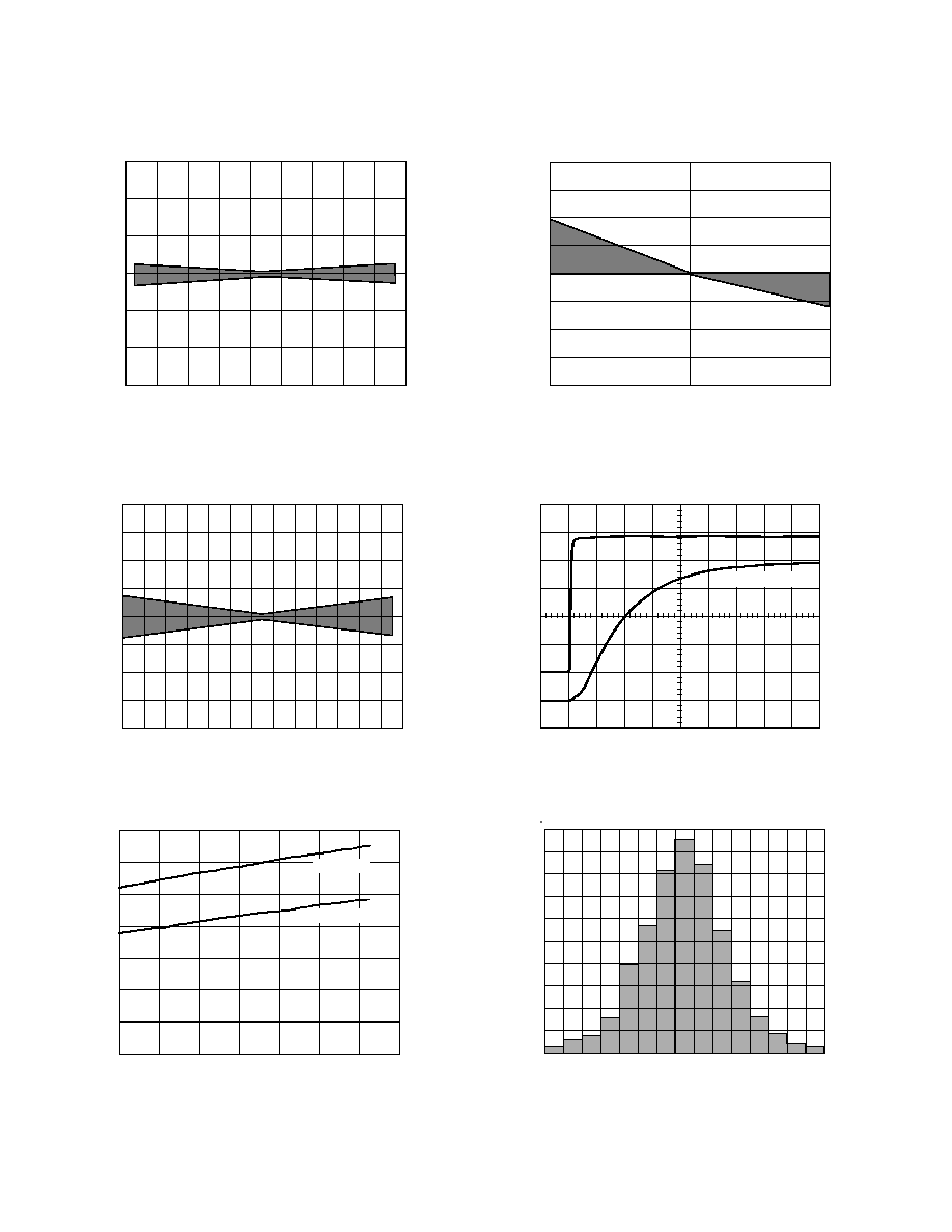
Figure 2. Normalized DCM Period (T2) vs. Temperature
TEMPERATURE ≠ C
0.8
≠0.2
≠0.8
≠40
90
≠30
ZERO
g
OFFSET SHIFT IN
g
≠20 ≠10
0
10
20
30
40
50
60
70
80
0.6
0
≠0.4
≠0.6
0.4
0.2
Figure 3. Typical Zero g Offset vs. Temperature
TEMPERATURE ≠ C
0.7
0
≠40
100
≠20
SUPPLY CURRENT ≠ mA
0
20
40
60
80
0.6
0.4
0.3
0.2
0.1
0.5
V
S
= 5 VDC
V
S
= 3.5 VDC
Figure 4. Typical Supply Current vs. Temperature
(@ +25 C R
SET
= 125 k
, V
DD
= +5 V, unless otherwise noted)
TYPICAL CHARACTERISTICS
TEMPERATURE ≠ C
4%
3%
≠4%
≠40
85
25
0%
≠1%
≠2%
≠3%
2%
1%
CHANGE IN SENSITIVITY
Figure 5. Typical X Axis Sensitivity Drift Due to
Temperature
0
0.4
0.8
1.2
1.4
FREQUENCY ≠ ms
3
2
1
0
VOLTS
C
FILT
= 0.01 F
Figure 6. Typical Turn-On Time
g/DUTY CYCLE OUTPUT
20
6
0
≠0.87g
PERCENTAGE OF SAMPLES
≠0.64g
≠0.41g ≠0.17g
0.06g
0.29g
0.52g
0.75g
18
8
4
2
14
10
16
12
Figure 7. Typical Zero g Distribution at +25
∞
C

ADXL202/ADXL210
≠5≠
REV. B
DUTY CYCLE OUTPUT ≠ % per
g
11.3
11.5 11.7 11.9 12.2 12.4 12.6 12.8 13.1 13.3 13.5 13.7
9
8
0
PERCENTAGE OF SAMPLES
4
3
2
1
6
5
7
Figure 8. Typical Sensitivity per g at +25
∞
C
C
X
, C
Y
BANDWIDTH
14
12
0
0.01 F
500Hz
0.47 F
10Hz
0.047 F
100Hz
TOTAL RMS NOISE ≠ m
g
0.1 F
50Hz
8
6
4
2
10
Figure 9. Typical Noise at X
FILT
Output
NUMBER OF AVERAGE SAMPLES
14
12
0
1
64
4
TOTAL RMS NOISE ≠ m
g
16
8
6
4
2
10
C
FILT
= 0.047 F
BW = 100Hz
C
FILT
= 0.1 F
BW = 50Hz
C
FILT
= 0.47 F
BW = 10Hz
C
FILT
= 0.01 F
BW = 500Hz
T2 = 1ms
Figure 10. Typical Noise at Digital Outputs
DEGREES OF MISALIGNMENT
20
6
0
≠1.375
0.375
% OF PARTS
≠1.125
≠0.875
≠0.625
≠0.375
≠0.0125
18
8
4
2
16
12
14
10
0.625
0.875
1.125
1.375
0.0125
Figure 11. Rotational Die Alignment