 | ÐлекÑÑоннÑй компоненÑ: AMP04 | СкаÑаÑÑ:  PDF PDF  ZIP ZIP |
Äîêóìåíòàöèÿ è îïèñàíèÿ www.docs.chipfind.ru
REV. A
Information furnished by Analog Devices is believed to be accurate and
reliable. However, no responsibility is assumed by Analog Devices for its
use, nor for any infringements of patents or other rights of third parties
which may result from its use. No license is granted by implication or
otherwise under any patent or patent rights of Analog Devices.
a
AMP04*
One Technology Way, P.O. Box 9106, Norwood, MA 02062-9106, U.S.A.
Tel: 617/329-4700
Fax: 617/326-8703
FUNCTIONAL BLOCK DIAGRAM
2
3
8
1
6
5
IN()
IN(+)
INPUT BUFFERS
R
GAIN
100k
REF
100k
V
OUT
11k
11k
FEATURES
Single Supply Operation
Low Supply Current: 700 A max
Wide Gain Range: 1 to 1000
Low Offset Voltage: 150 V max
Zero-In/Zero-Out
Single-Resistor Gain Set
8-Pin Mini-DIP and SO packages
APPLICATIONS
Strain Gages
Thermocouples
RTDs
Battery Powered Equipment
Medical Instrumentation
Data Acquisition Systems
PC Based Instruments
Portable Instrumentation
Precision Single Supply
Instrumentation Amplifier
GENERAL DESCRIPTION
The AMP04 is a single-supply instrumentation amplifier
designed to work over a +5 volt to
±
15 volt supply range. It
offers an excellent combination of accuracy, low power con-
sumption, wide input voltage range, and excellent gain
performance.
Gain is set by a single external resistor and can be from 1 to
1000. Input common-mode voltage range allows the AMP04 to
handle signals with full accuracy from ground to within 1 volt of
the positive supply. And the output can swing to within 1 volt of
the positive supply. Gain bandwidth is over 700 kHz. In addi-
tion to being easy to use, the AMP04 draws only 700
µ
A of sup-
ply current.
For high resolution data acquisition systems, laser trimming of
low drift thin-film resistors limits the input offset voltage to
under 150
µ
V, and allows the AMP04 to offer gain nonlinearity
of 0.005% and a gain tempco of 30 ppm/
°
C.
A proprietary input structure limits input offset currents to less
than 5 nA with drift of only 8 pA/
°
C, allowing direct connection
of the AMP04 to high impedance transducers and other signal
sources.
*Protected by U.S. Patent No. 5,075,633.
The AMP04 is specified over the extended industrial (40
°
C to
+85
°
C) temperature range. AMP04s are available in plastic and
ceramic DIP plus SO-8 surface mount packages.
Contact your local sales office for MIL-STD-883 data sheet
and availability.
PIN CONNECTIONS
8-Lead Epoxy DIP
(P Suffix)
8-Lead Narrow-Body SO
(S Suffix)
1
2
3
4
8
7
6
5
AMP-04
R
GAIN
V+
V
OUT
REF
R
GAIN
IN
+IN
V
AMP-04
V+
R
GAIN
V
OUT
REF
R
GAIN
IN
+IN
V

AMP04SPECIFICATIONS
ELECTRICAL CHARACTERISTICS
AMP04E
AMP04F
Parameter
Symbol
Conditions
Min
Typ
Max
Min
Typ
Max
Units
OFFSET VOLTAGE
Input Offset Voltage
V
IOS
30
150
300
µ
V
40
°
C
T
A
+85
°
C
300
600
µ
V
Input Offset Voltage Drift
TCV
IOS
3
6
µ
V/
°
C
Output Offset Voltage
V
OOS
0.5
1.5
3
mV
40
°
C
T
A
+85
°
C
3
6
mV
Output Offset Voltage Drift
TCVoos
30
50
µ
V/
°
C
INPUT CURRENT
Input Bias Current
I
B
22
30
40
nA
40
°
C
T
A
+85
°
C
50
60
nA
Input Bias Current Drift
TCI
B
65
65
pA/
°
C
Input Offset Current
I
OS
1
5
10
nA
40
°
C
T
A
+85
°
C
10
15
nA
Input Offset Current Drift
TCI
OS
8
8
pA/
°
C
INPUT
Common-Mode Input Resistance
4
4
G
Differential Input Resistance
4
4
G
Input Voltage Range
V
IN
0
3.0
0
3.0
V
Common-Mode Rejection
CMR
0 V
V
CM
3.0 V
G = 1
60
80
55
dB
G = 10
80
100
75
dB
G = 100
90
105
80
dB
G = 1000
90
105
80
dB
Common-Mode Rejection
CMR
0 V
V
CM
2.5 V
40
°
C
T
A
+85
°
C
G = 1
55
50
dB
G = 10
75
70
dB
G = 100
85
75
dB
G = 1000
85
75
dB
Power Supply Rejection
PSRR
4.0 V
V
S
12 V
40
°
C
T
A
+85
°
C
G = 1
95
85
dB
G = 10
105
95
dB
G = 100
105
95
dB
G = 1000
105
95
dB
GAIN (G = 100 K/R
GAIN
)
Gain Equation Accuracy
G = 1 to 100
0.2
0.5
0.75
%
G = 1 to 100
40
°
C
T
A
+85
°
C
0.8
1.0
%
G = 1000
0.4
0.75
%
Gain Range
G
1
1000
1
1000
V/V
Nonlinearity
G = 1, R
L
= 5 k
0.005
%
G = 10, R
L
= 5 k
0.015
%
G = 100, R
L
= 5 k
0.025
%
Gain Temperature Coefficient
G/
T
30
50
ppm/
°
C
OUTPUT
Output Voltage Swing High
V
OH
R
L
= 2 k
4.0
4.2
4.0
V
R
L
= 2 k
40
°
C
T
A
+85
°
C
3.8
3.8
V
Output Voltage Swing Low
V
OL
R
L
= 2 k
40
°
C
T
A
+85
°
C
2.0
2.5
mV
Output Current Limit
Sink
30
30
mA
Source
15
15
mA
REV. A
2
(V
S
= +5 V, V
CM
= +2.5 V, T
A
= +25 C unless otherwise noted)
AMP04
REV. A
3
AMP04E
AMP04F
Parameter
Symbol
Conditions
Min
Typ
Max
Min
Typ
Max
Units
NOISE
Noise Voltage Density, RTI
e
N
f = 1 kHz, G = 1
270
270
nV/
Hz
f = 1 kHz, G = 10
45
45
nV/
Hz
f = 100 Hz, G = 100
30
30
nV/
Hz
f = 100 Hz, G = 1000
25
25
nV/
Hz
Noise Current Density, RTI
i
N
f = 100 Hz, G = 100
4
4
pA/
Hz
Input Noise Voltage
e
N
p-p
0.1 to 10 Hz, G = 1
7
7
µ
V p-p
0.1 to 10 Hz, G = 10
1.5
1.5
µ
V p-p
0.1 to 10 Hz, G = 100
0.7
0.7
µ
V p-p
DYNAMIC RESPONSE
Small Signal Bandwidth
BW
G = 1, 3 dB
300
300
kHz
POWER SUPPLY
Supply Current
I
SY
550
700
700
µ
A
40
°
C
T
A
+85
°
C
850
850
µ
A
Specifications subject to change without notice.
ELECTRICAL CHARACTERISTICS
AMP04E
AMP04F
Parameter
Symbol
Conditions
Min
Typ
Max
Min
Typ
Max
Units
OFFSET VOLTAGE
Input Offset Voltage
V
IOS
80
400
600
µ
V
40
°
C
T
A
+85
°
C
600
900
µ
V
Input Offset Voltage Drift
TCV
IOS
3
6
µ
V/
°
C
Output Offset Voltage
V
OOS
1
3
6
mV
40
°
C
T
A
+85
°
C
6
9
mV
Output Offset Voltage Drift
TCVoos
30
50
µ
V/
°
C
INPUT CURRENT
Input Bias Current
I
B
17
30
40
nA
40
°
C
T
A
+85
°
C
50
60
nA
Input Bias Current Drift
TCI
B
65
65
pA/
°
C
Input Offset Current
I
OS
2
5
10
nA
40
°
C
T
A
+85
°
C
15
20
nA
Input Offset Current Drift
TCI
OS
28
28
pA/
°
C
INPUT
Common-Mode Input Resistance
4
4
G
Differential Input Resistance
4
4
G
Input Voltage Range
V
IN
12
+12
12
+12
V
Common-Mode Rejection
CMR
12 V
V
CM
+12 V
G = 1
60
80
55
dB
G = 10
80
100
75
dB
G = 100
90
105
80
dB
G = 1000
90
105
80
dB
Common-Mode Rejection
CMR
11 V
V
CM
+11 V
40
°
C
T
A
+85
°
C
G = 1
55
50
dB
G = 10
75
70
dB
G = 100
85
75
dB
G = 1000
85
75
dB
Power Supply Rejection
PSRR
±
2.5 V
V
S
±
18 V
40
°
C
T
A
+85
°
C
G = 1
75
70
dB
G = 10
90
80
dB
G = 100
95
85
dB
G = 1000
95
85
dB
(V
S
= 5 V, V
CM
= 0 V, T
A
= +25 C unless otherwise noted)
AMP04
REV. A
4
AMP04E
AMP04F
Parameter
Symbol
Conditions
Min
Typ
Max
Min
Typ
Max
Units
GAIN (G = 100 K/R
GAIN
)
Gain Equation Accuracy
G = 1 to 100
0.2
0.5
0.75
%
G = 1000
0.4
0.75
%
G = 1 to 100
40
°
C
T
A
+85
°
C
0.8
1.0
%
Gain Range
G
1
1000
1
1000
V/V
Nonlinearity
G = 1, R
L
= 5 k
0.005
0.005
%
G = 10, R
L
= 5 k
0.015
0.015
%
G = 100, R
L
= 5 k
0.025
0.025
%
Gain Temperature Coefficient
G/
T
30
50
ppm/
°
C
OUTPUT
Output Voltage Swing High
V
OH
R
L
= 2 k
+13
+13.4
+13
V
R
L
= 2 k
40
°
C
T
A
+85
°
C
+12.5
+12.5
V
Output Voltage Swing Low
V
OL
R
L
= 2 k
40
°
C
T
A
+85
°
C
14.5
14.5 V
Output Current Limit
Sink
30
30
mA
Source
15
15
mA
NOISE
Noise Voltage Density, RTI
e
N
f = 1 kHz, G = 1
270
270
nV/
Hz
f = 1 kHz, G = 10
45
45
nV/
Hz
f = 100 Hz, G = 100
30
30
nV/
Hz
f = 100 Hz, G = 1000
25
25
nV/
Hz
Noise Current Density, RTI
i
N
f = 100 Hz, G = 100
4
4
pA/
Hz
Input Noise Voltage
e
N
p-p
0.1 to 10 Hz, G = 1
5
5
µ
V p-p
0.1 to 10 Hz, G = 10
1
1
µ
V p-p
0.1 to 10 Hz, G = 100
0.5
0.5
µ
V p-p
DYNAMIC RESPONSE
Small Signal Bandwidth
BW
G = 1, 3 dB
700
700
kHz
POWER SUPPLY
Supply Current
I
SY
750
900
900
µ
A
40
°
C
T
A
+85
°
C
1100
1100
µ
A
Specifications subject to change without notice.
WAFER TEST LIMITS
Parameter
Symbol
Conditions
Limit
Units
OFFSET VOLTAGE
Input Offset Voltage
V
IOS
300
µ
V max
Output Offset Voltage
V
OOS
3
mV max
INPUT CURRENT
Input Bias Current
I
B
40
nA max
Input Offset Current
I
OS
10
nA max
INPUT
Common-Mode Rejection
CMR
0 V
V
CM
3.0 V
G = 1
55
dB min
G = 10
75
dB min
G = 100
80
dB min
G = 1000
80
dB min
Common-Mode Rejection
CMR
V
S
=
±
15 V, 12 V
V
CM
+12 V
G = 1
55
dB min
G = 10
75
dB min
G = 100
80
dB min
(V
S
= +5 V, V
CM
= +2.5 V, T
A
= +25 C unless otherwise noted)
AMP04
REV. A
5
Parameter
Symbol
Conditions
Limit
Units
G = 1000
80
dB min
Power Supply Rejection
PSRR
4.0 V
V
S
12 V
G = 1
85
dB min
G = 10
95
dB min
G = 100
95
dB min
G = 1000
95
dB min
GAIN (G = 100 K/R
GAIN
)
Gain Equation Accuracy
G = 1 to 100
0.75
% max
OUTPUT
Output Voltage Swing High
V
OH
R
L
= 2 k
4.0
V min
Output Voltage Swing Low
V
OL
R
L
= 2 k
2.5
mV max
POWER SUPPLY
Supply Current
I
SY
V
S
=
±
15
900
µ
A max
700
µ
A max
NOTE
Electrical tests and wafer probe to the limits shown. Due to variations in assembly methods and normal yield loss, yield after packaging is not guaranteed for standard
product dice. Consult factory to negotiate specifications based on dice lot qualifications through sample lot assembly and testing.
ABSOLUTE MAXIMUM RATINGS
1
Supply Voltage . . . . . . . . . . . . . . . . . . . . . . . . . . . . . . . . .
±
18 V
Common-Mode Input Voltage
2
. . . . . . . . . . . . . . . . . .
±
18 V
Differential Input Voltage . . . . . . . . . . . . . . . . . . . . . . . . . 36 V
Output Short-Circuit Duration to GND . . . . . . . . . . Indefinite
Storage Temperature Range
Z Package . . . . . . . . . . . . . . . . . . . . . . . . . . 65
°
C to +175
°
C
P, S Package . . . . . . . . . . . . . . . . . . . . . . . . 65
°
C to +150
°
C
Operating Temperature Range
AMP04A . . . . . . . . . . . . . . . . . . . . . . . . . . 55
°
C to +125
°
C
AMP04E, F . . . . . . . . . . . . . . . . . . . . . . . . . 40
°
C to +85
°
C
Junction Temperature Range
Z Package . . . . . . . . . . . . . . . . . . . . . . . . . . 65
°
C to +175
°
C
P, S Package . . . . . . . . . . . . . . . . . . . . . . . . 65
°
C to +150
°
C
Lead Temperature Range (Soldering, 60 sec) . . . . . . . +300
°
C
Package Type
JA
3
JC
Units
8-Pin Cerdip (Z)
148
16
°
C/W
8-Pin Plastic DIP (P)
103
43
°
C/W
8-Pin SOIC (S)
158
43
°
C/W
NOTES
1
Absolute maximum ratings apply to both DICE and packaged parts, unless
otherwise noted.
2
For supply voltages less than
±
18 V, the absolute maximum input voltage is
equal to the supply voltage.
3
JA
is specified for the worst case conditions, i.e.,
JA
is specified for device in
socket for cerdip, P-DIP, and LCC packages;
JA
is specified for device
soldered in circuit board for SOIC package.
ORDERING GUIDE
Temperature
V
OS
@ +5 V
Package
Package
Model
Range
T
A
= +25 C
Description
Option
AMP04EP
XIND
150
µ
V
Plastic DIP
N-8
AMP04ES
XIND
150
µ
V
SOIC
SO-8
AMP04FP
XIND
300
µ
V
Plastic DIP
N-8
AMP04FS
XIND
300
µ
V
SOIC
SO-8
AMP04FS-REEL
XIND
150
µ
V
SOIC
SO-8
AMP04FS-REEL7
XIND
150
µ
V
SOIC
SO-8
AMP04GBC
+25
°
C
300
µ
V
DICE CHARACTERISTICS
AMP04 Die Size 0.075
×
0.99 inch, 7,425 sq. mils.
Substrate (Die Backside) Is Connected to V+.
Transistor Count, 81.
AMP04
REV. A
6
APPLICATIONS
Common-Mode Rejection
The purpose of the instrumentation amplifier is to amplify the
difference between the two input signals while ignoring offset
and noise voltages common to both inputs. One way of judging
the device's ability to reject this offset is the common-mode
gain, which is the ratio between a change in the common-mode
voltage and the resulting output voltage change. Instrumenta-
tion amplifiers are often judged by the common-mode rejection
ratio, which is equal to 20
×
log
10
of the ratio of the user-selected
differential signal gain to the common-mode gain, commonly
called the CMRR. The AMP04 offers excellent CMRR, guaran-
teed to be greater than 90 dB at gains of 100 or greater. Input
offsets attain very low temperature drift by proprietary laser-
trimmed thin-film resistors and high gain amplifiers.
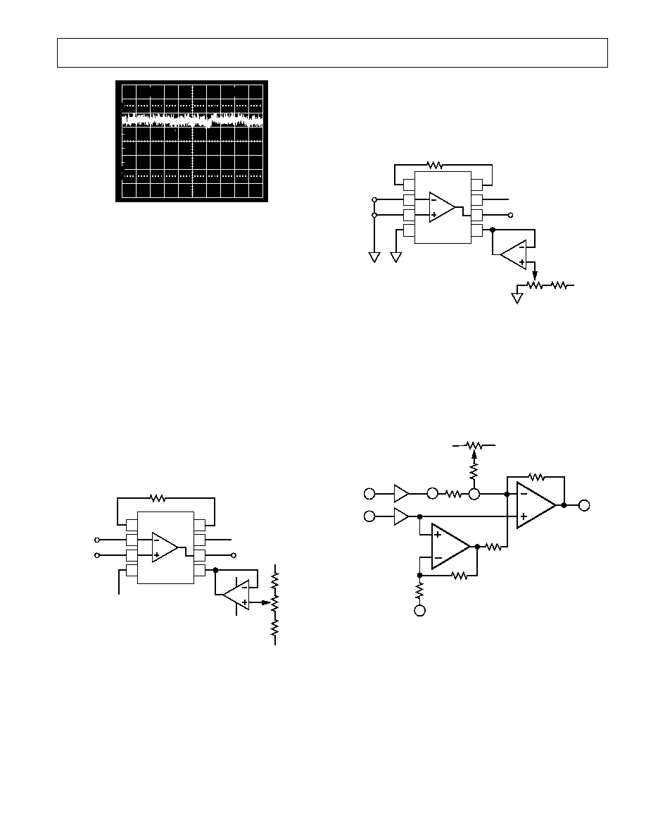
Input Common-Mode Range Includes Ground
The AMP04 employs a patented topology (Figure 1) that
uniquely allows the common-mode input voltage to truly extend
to zero volts where other instrumentation amplifiers fail. To il-
lustrate, take for example the single supply, gain of 100 instru-
mentation amplifier as in Figure 2. As the inputs approach zero
volts, in order for the output to go positive, amplifier A's output
(V
OA
) must be allowed to go below ground, to 0.094 volts.
Clearly this is not possible in a single supply environment. Con-
sequently this instrumentation amplifier configuration's input
common-mode voltage cannot go below about 0.4 volts. In
comparison, the AMP04 has no such restriction. Its inputs will
function with a zero-volt common-mode voltage.
2
3
8
1
6
5
IN()
IN(+)
INPUT BUFFERS
R
GAIN
100k
REF
100k
V
OUT
11k
11k
Figure 1. Functional Block Diagram
B
A
V
OA
100k
20k
20k
100k
2127
0V
V
OUT
0V
0.01V
0.01V
+
4.7
µ
A
5.2
µ
A
4.7
µ
A
V
OB
.094V
V
IN
Figure 2. Gain = 100 Instrumentation Amplifier
Input Common-Mode Voltage Below Ground
Although not tested and guaranteed, the AMP04 inputs are bi-
ased in a way that they can amplify signals linearly with common-
mode voltage as low as 0.25 volts below ground. This holds
true over the industrial temperature range from 40
°
C to +85
°
C.
Extended Positive Common-Mode Range
On the high side, other instrumentation amplifier configura-
tions, such as the three op amp instrumentation amplifier, can
have severe positive common-mode range limitations. Figure 3
shows an example of a gain of 1001 amplifier, with an input
common-mode voltage of 10 volts. For this circuit to function,
V
OB
must swing to 15.01 volts in order for the output to go to
10.01 volts. Clearly no op amp can handle this swing range
(given a +15 V supply) as the output will saturate long before it
reaches the supply rails. Again the AMP04's topology does not
have this limitation. Figure 4 illustrates the AMP04 operating at
the same common-mode conditions as in Figure 3. None of the
internal nodes has a signal high enough to cause amplifier satu-
ration. As a result, the AMP04 can accommodate much wider
common-mode range than most instrumentation amplifiers.
B
V
OA
100k
100k
A
V
OB
R
R
R
+5V
+15.01V
R
10.01
+10.00V
+10.01V
200
50
µ
A
Figure 3. Gain = 1001, Three Op Amp Instrumentation
Amplifier
+10.00V
+10.01V
100k
100k
V
OUT
11k
15V
+10.01V
100
100
µ
A
+15V
11k
+11.111V
+
0.1
µ
A
100.1
µ
A
15V
+15V
+10V
Figure 4. Gain = 1000, AMP04
AMP04
REV. A
7
Programming the Gain
The gain of the AMP04 is programmed by the user by selecting
a single external resistor--R
GAIN
:
Gain = 100 k
/R
GAIN
The output voltage is then defined as the differential input volt-
age times the gain.
V
OUT
= (V
IN+
V
IN
)
×
Gain
In single supply systems, offsetting the ground is often desired
for several reasons. Ground may be offset from zero to provide
a quieter signal reference point, or to offset "zero" to allow a
unipolar signal range to represent both positive and negative
values.
In noisy environments such as those having digital switching,
switching power supplies or externally generated noise, ground
may not be the ideal place to reference a signal in a high accu-
racy system.
Often, real world signals such as temperature or pressure may
generate voltages that are represented by changes in polarity. In
a single supply system the signal input cannot be allowed to go
below ground, and therefore the signal must be offset to accom-
modate this change in polarity. On the AMP04, a reference in-
put pin is provided to allow offsetting of the input range.
The gain equation is more accurately represented by including
this reference input.
V
OUT
= (V
IN+
V
IN
)
×
Gain + V
REF
Grounding
The most common problems encountered in high performance
analog instrumentation and data acquisition system designs are
found in the management of offset errors and ground noise.
Primarily, the designer must consider temperature differentials
and thermocouple effects due to dissimilar metals, IR voltage
drops, and the effects of stray capacitance. The problem is
greatly compounded when high speed digital circuitry, such as
that accompanying data conversion components, is brought
into the proximity of the analog section. Considerable noise and
error contributions such as fast-moving logic signals that easily
propagate into sensitive analog lines, and the unavoidable noise
common to digital supply lines must all be dealt with if the accu-
racy of the carefully designed analog section is to be preserved.
Besides the temperature drift errors encountered in the ampli-
fier, thermal errors due to the supporting discrete components
should be evaluated. The use of high quality, low-TC compo-
nents where appropriate is encouraged. What is more important,
large thermal gradients can create not only unexpected changes
in component values, but also generate significant thermoelec-
tric voltages due to the interface between dissimilar metals such
as lead solder, copper wire, gold socket contacts, Kovar lead
frames, etc. Thermocouple voltages developed at these junc-
tions commonly exceed the TCV
OS
contribution of the
AMP04. Component layout that takes into account the power
dissipation at critical locations in the circuit and minimizes gra-
dient effects and differential common-mode voltages by taking
advantage of input symmetry will minimize many of these errors.
High accuracy circuitry can experience considerable error con-
tributions due to the coupling of stray voltages into sensitive
areas, including high impedance amplifier inputs which benefit
from such techniques as ground planes, guard rings, and
shields. Careful circuit layout, including good grounding and
signal routing practice to minimize stray coupling and ground
loops is recommended. Leakage currents can be minimized by
using high quality socket and circuit board materials, and by
carefully cleaning and coating complete board assemblies.
As mentioned above, the high speed transition noise found in
logic circuitry is the sworn enemy of the analog circuit designer.
Great care must be taken to maintain separation between them
to minimize coupling. A major path for these error voltages will
be found in the power supply lines. Low impedance, load re-
lated variations and noise levels that are completely acceptable
in the high thresholds of the digital domain make the digital
supply unusable in nearly all high performance analog applica-
tions. The user is encouraged to maintain separate power and
ground between the analog and digital systems wherever pos-
sible, joining only at the supply itself if necessary, and to ob-
serve careful grounding layout and bypass capacitor scheduling
in sensitive areas.
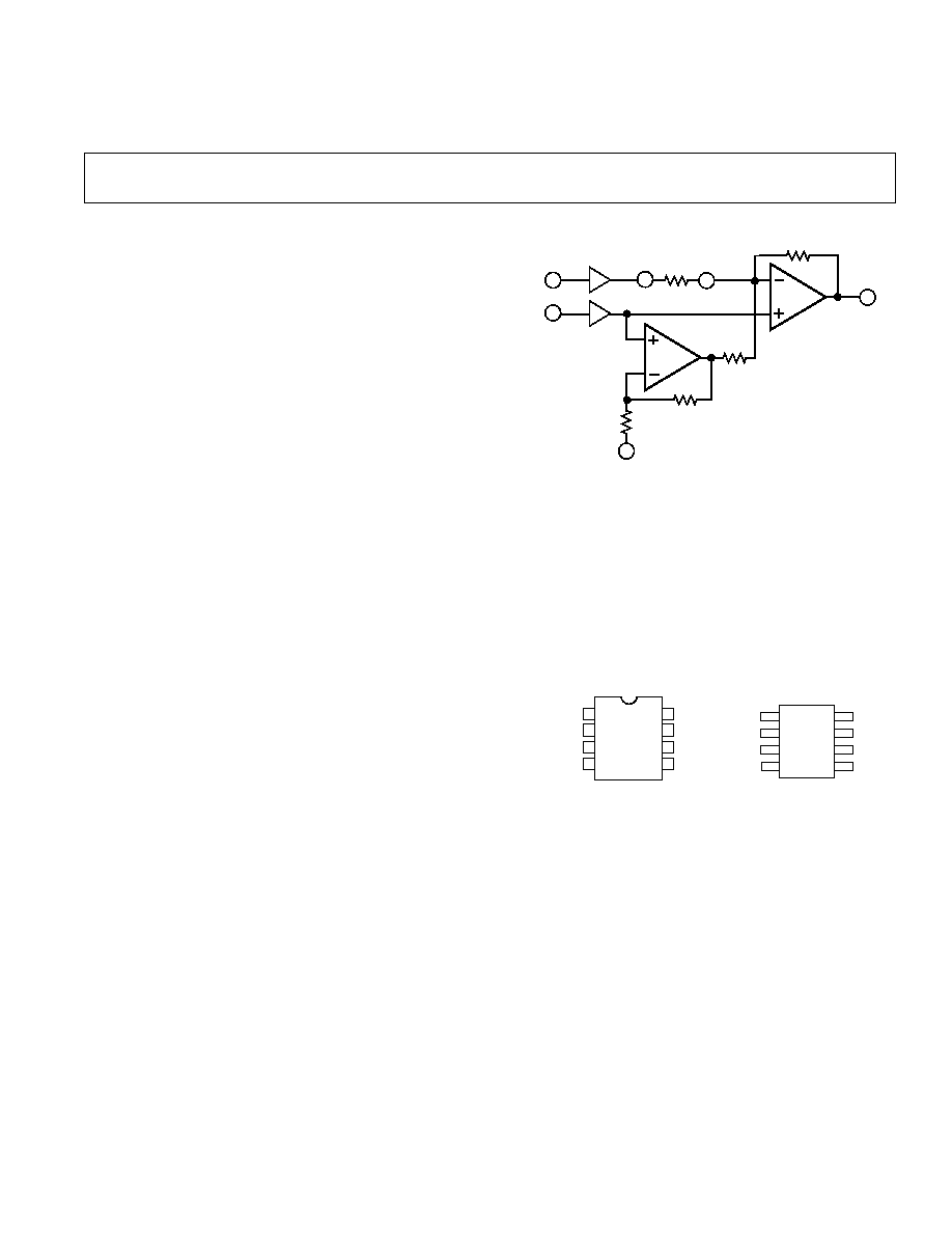
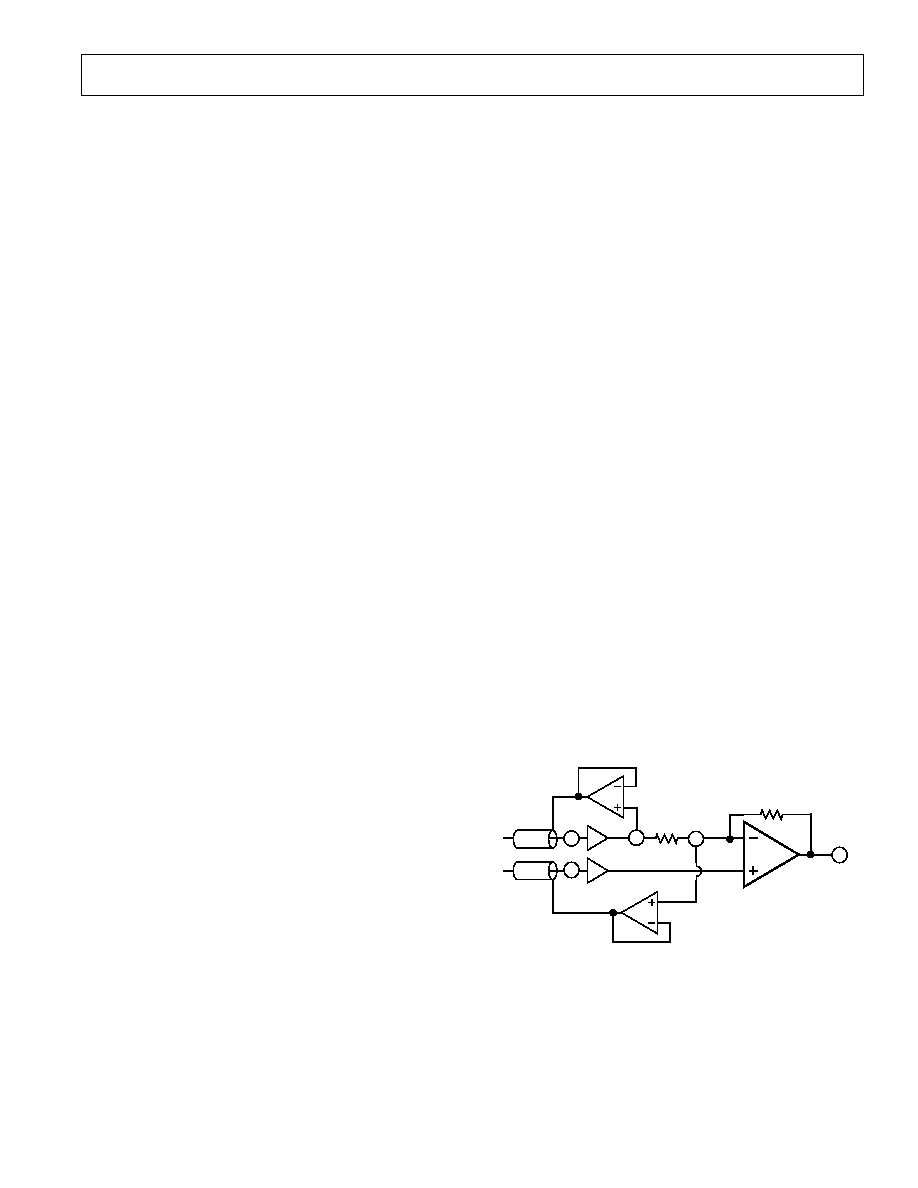
Input Shield Drivers
High impedance sources and long cable runs from remote trans-
ducers in noisy industrial environments commonly experience
significant amounts of noise coupled to the inputs. Both stray
capacitance errors and noise coupling from external sources can
be minimized by running the input signal through shielded
cable. The cable shield is often grounded at the analog input
common, however improved dynamic noise rejection and a re-
duction in effective cable capacitance is achieved by driving the
shield with a buffer amplifier at a potential equal to the voltage
seen at the input. Driven shields are easily realized with the
AMP04. Examination of the simplified schematic shows that the
potentials at the gain set resistor pins of the AMP04 follow the
inputs precisely. As shown in Figure 5, shield drivers are easily
realized by buffering the potential at these pins by a dual, single
supply op amp such as the OP213. Alternatively, applications
with single-ended sources or that use twisted-pair cable could
drive a single shield. To minimize error contributions due to
this additional circuitry, all components and wiring should re-
main in proximity to the AMP04 and careful grounding and by-
passing techniques should be observed.
2
3
8
1
6
V
OUT
1/2 OP-213
1/2 OP-213
Figure 5. Cable Shield Drivers
AMP04
REV. A
8
Compensating for Input and Output Errors
To achieve optimal performance, the user needs to take into
account a number of error sources found in instrumentation
amplifiers. These consist primarily of input and output offset
voltages and leakage currents.
The input and output offset voltages are independent from one
another, and must be considered separately. The input offset
component will of course be directly multiplied by the gain of
the amplifier, in contrast to the output offset voltage that is in-
dependent of gain. Therefore, the output error is the dominant
factor at low gains, and the input error grows to become the
greater problem as gain is increased. The overall equation for
offset voltage error referred to the output (RTO) is:
V
OS
(RTO) = (V
IOS
×
G) + V
OOS
where V
IOS
is the input offset voltage and V
OOS
the output offset
voltage, and G is the programmed amplifier gain.
The change in these error voltages with temperature must also
be taken into account. The specification TCV
OS
, referred to the
output, is a combination of the input and output drift specifica-
tions. Again, the gain influences the input error but not the out-
put, and the equation is:
TCV
OS
(RTO) = (TCV
IOS
×
G) + TCV
OOS
In some applications the user may wish to define the error con-
tribution as referred to the input, and treat it as an input error.
The relationship is:
TCV
OS
(RTI) = TCV
IOS
+ (TCV
OOS
/ G)
The bias and offset currents of the input transistors also have an
impact on the overall accuracy of the input signal. The input
leakage, or bias currents of both inputs will generate an addi-
tional offset voltage when flowing through the signal source re-
sistance. Changes in this error component due to variations with
signal voltage and temperature can be minimized if both input
source resistances are equal, reducing the error to a common-
mode voltage which can be rejected. The difference in bias cur-
rent between the inputs, the offset current, generates a differen-
tial error voltage across the source resistance that should be
taken into account in the user's design.
In applications utilizing floating sources such as thermocouples,
transformers, and some photo detectors, the user must take care
to provide some current path between the high impedance in-
puts and analog ground. The input bias currents of the AMP04,
although extremely low, will charge the stray capacitance found
in nearby circuit traces, cables, etc., and cause the input to drift
erratically or to saturate unless given a bleed path to the analog
common. Again, the use of equal resistance values will create a
common input error voltage that is rejected by the amplifier.
Reference Input
The V
REF
input is used to set the system ground. For dual sup-
ply operation it can be connected to ground to give zero volts
out with zero volts differential input. In single supply systems it
could be connected either to the negative supply or to a pseudo-
ground between the supplies. In any case, the REF input must
be driven with low impedance.
Noise Filtering
Unlike most previous instrumentation amplifiers, the output
stage's inverting input (Pin 8) is accessible. By placing a capaci-
tor across the AMP04's feedback path (Figure 6, Pins 6 and 8)
2
3
8
1
6
5
IN()
IN(+)
INPUT BUFFERS
R
GAIN
100k
REF
100k
V
OUT
11k
11k
R
GAIN
C
EXT
LP
=
1
2
(100k) C
EXT
Figure 6. Noise Band Limiting
a single-pole low-pass filter is produced. The cutoff frequency
(f
LP
) follows the relationship:
f
LP
=
1
2
(100 k
) C
EXT
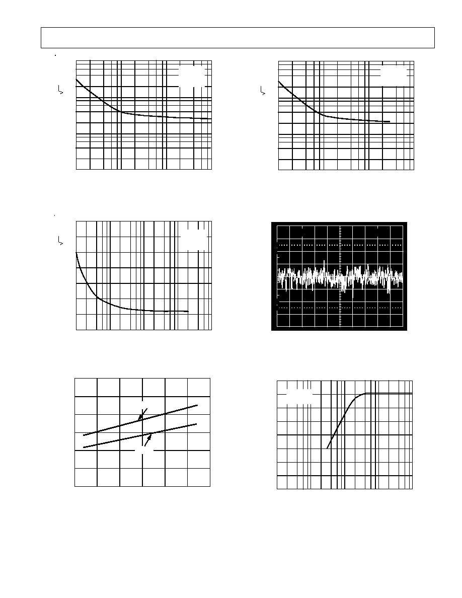
Filtering can be applied to reduce wide band noise. Figure 7a
shows a 10 Hz low-pass filter, gain of 1000 for the AMP04. Fig-
ures 7b and 7c illustrate the effect of filtering on noise. The
photo in Figure 7b shows the output noise before filtering. By
adding a 0.15
µ
F capacitor, the noise is reduced by about a
factor of 4 as shown in Figure 7c.
7
1
6
5
4
3
2
8
+15V
15V
100
0.15
µ
F
Figure 7a. 10 Hz Low-Pass Filter
10
90
100
0%
5mV
10ms
Figure 7b. Unfiltered AMP04 Output
AMP04
REV. A
9
10
90
100
0%
1mV
2s
Figure 7c. 10 Hz Low-Pass Filtered Output
Power Supply Considerations
In dual supply applications (for example
±
15 V) if the input is
connected to a low resistance source less than 100
, a large
current may flow in the input leads if the positive supply is ap-
plied before the negative supply during power-up. A similar
condition may also result upon a loss of the negative supply. If
these conditions could be present in you system, it is recom-
mended that a series resistor up to 1 k
be added to the input
leads to limit the input current.
This condition can not occur in a single supply environment as
losing the negative supply effectively removes any current return
path.
Offset Nulling in Dual Supply
Offset may be nulled by feeding a correcting voltage at the V
REF
pin (Pin 5). However, it is important that the pin be driven with
a low impedance source. Any measurable resistance will degrade
the amplifier's common-mode rejection performance as well as
its gain accuracy. An op amp may be used to buffer the offset
null circuit as in Figure 8.
1
2
3
4
8
7
6
5
AMP-04
V
REF
V+
R
G
+
INPUT
5V
5V
+5V
50k
50k
100
+5V
5V
OUTPUT
+5V
±
5mV
ADJ
RANGE
* OP-90 FOR LOW POWER
OP-113 FOR LOW DRIFT
*
Figure 8. Offset Adjust for Dual Supply Applications
Offset Nulling in Single Supply
Nulling the offset in single supply systems is difficult because
the adjustment is made to try to attain zero volts. At zero volts
out, the output is in saturation (to the negative rail) and the out-
put voltage is indistinguishable from the normal offset error.
Consequently the offset nulling circuit in Figure 9 must be used
with caution.
First, the potentiometer should be adjusted to cause the
output to swing in the positive direction; then adjust it in
the reverse direction, causing the output to swing toward
ground, until the output just stops changing. At that point
the output is at the saturation limit.
1
2
3
4
8
7
6
5
AMP-04
R
G
INPUT
50k
100
+5V
OUTPUT
+5V
OP-113
Figure 9. Offset Adjust for Single Supply Applications
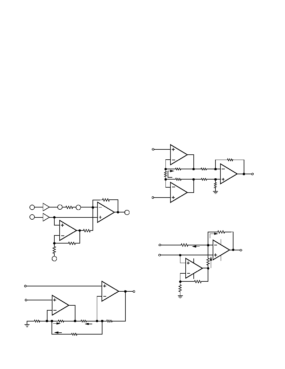
Alternative Nulling Method
An alternative null correction technique is to inject an off-
set current into the summing node of the output amplifier
as in Figure 10. This method does not require an external
op amp. However the drawback is that the amplifier will
move off its null as the input common-mode voltage
changes. It is a less desirable nulling circuit than the previ-
ous method.
2
3
8
1
6
5
IN()
IN(+)
INPUT BUFFERS
R
GAIN
100k
REF
100k
V
OUT
11k
11k
V+
V
Figure 10. Current Injection Offsetting Is Not
Recommended
AMP04
REV. A
10
APPLICATION CIRCUITS
Low Power Precision Single Supply RTD Amplifier
Figure 11 shows a linearized RTD amplifier that is powered off
a single +5 volt supply. However, the circuit will work up to 36
volts without modification. The RTD is excited by a 100
µ
A
constant current that is regulated by amplifier A (OP295). The
0.202 volts reference voltage used to generate the constant cur-
rent is divided down from the 2.500 volt reference. The AMP04
amplifies the bridge output to a 10 mV/
°
C output coefficient.
100
7
1
6
5
4
2
3
8
+5V
AMP-04
8
7
4
5
6
+5V
50k
R7
121k
1/2
OP-295
1/2
OP-295
A
B
REF-43
GND
OUT
IN
6
4
2
2
3
1
+5V
C2
0.1
µ
F
R1
26.7k
R2
26.7k
R4
100
RTD
100
R
SENSE
1k
R9
50
R8
383
C3
0.1
µ
F
C1
0.47
µ
F
R10
R6
11.5k
2.5V
R5
1.02k
500
0.202V
V
OUT
FULL-SCALE
ADJ
0
4.00V
(0
°
C TO 400
°
C)
LINEARITY
ADJ.
(@1/2 FS)
NOTES: ALL RESISTORS
±
0.5%,
±
25 PPM/
°
C
ALL POTENTIOMETERS
±
25 PPM/
°
C
R3
BALANCE
Figure 11. Precision Single Supply RTD Thermometer
Amplifier
The RTD is linearized by feeding a portion of the signal back to
the reference circuit, increasing the reference voltage as the tem-
perature increases. When calibrated properly, the RTD's non-
linearity error will be canceled.
To calibrate, either immerse the RTD into a zero-degree ice
bath or substitute an exact 100
resistor in place of the RTD.
Then adjust bridge BALANCE potentiometer R3 for a 0 volt
output. Note that a 0 volt output is also the negative output
swing limit of the AMP04 powered with a single supply. There-
fore, be sure to adjust R3 to first cause the output to swing
positive and then back off until the output just stop swinging
negatively.
Next, set the LINEARITY ADJ. potentiometer to the mid-
range. Substitute an exact 247.04
resistor (equivalent to
400
°
C temperature) in place of the RTD. Adjust the
FULL-SCALE potentiometer for a 4.000 volts output.
Finally substitute a 175.84
resistor (equivalent to 200
°
C
temperature), and adjust the LINEARITY ADJ potentiometer
for a 2.000 volts at the output. Repeat the full-scale and the
half-scale adjustments as needed.
When properly calibrated, the circuit achieves better than
±
0.5
°
C accuracy within a temperature measurement range from
0
°
C to 400
°
C.
Precision 4-20 mA Loop Transmitter With Noninteractive
Trim
Figure 12 shows a full bridge strain gage transducer amplifier
circuit that is powered off the 4-20 mA current loop. The
AMP04 amplifies the bridge signal differentially and is con-
verted to a current by the output amplifier. The total quiescent
current drawn by the circuit, which includes the bridge, the am-
plifiers, and the resistor biasing, is only a fraction of the 4 mA
null current that flows through the current-sense resistor
R
SENSE
. The voltage across R
SENSE
feeds back to the OP90's in-
put, whose common-mode is fixed at the current summing
reference voltage, thus regulating the output current.
With no bridge signal, the 4 mA null is simply set up by the
50 k
NULL potentiometer plus the 976 k
resistors that in-
ject an offset that forces an 80 mV drop across R
SENSE
. At a
50 mV full-scale bridge voltage, the AMP04 amplifies the
voltage-to-current converter for a full-scale of 20 mA at the out-
put. Since the OP90's input operates at a constant 0 volt
common-mode voltage, the null and the span adjustments do
Figure 12. Precision 4-20 mA Loop Transmitter Features Noninteractive Trims
AMP04
REV. A
11
not interact with one another. Calibration is simple and easy
with the NULL adjusted first, followed by SPAN adjust. The
entire circuit can be remotely placed, and powered from the
4-20 mA 2-wire loop.
4-20 mA Loop Receiver
At the receiving end of a 4-20 mA loop, the AMP04 makes a
convenient differential receiver to convert the current back to a
usable voltage (Figure 13). The 4-20 mA signal current passes
through a 100
sense resistor. The voltage drop is differentially
amplified by the AMP04. The 4 mA offset is removed by the
offset correction circuit.
7
1
6
5
4
2
3
8
AMP-04
6
100k
0.15
µ
F
420mA
TRANS-
MITTER
POWER
SUPPLY
+
2
3
+
100
1%
1k
1k
WIRE RE-
SISTANCE
IN4002
0.400V
OP-177
AD589
10k
27k
15V
+15V
V
OUT
01.6V FS
15V
420mA
420mA
+
Figure 13. 4-to-20 mA Line Receiver
Low Power, Pulsed Load-Cell Amplifier
Figure 14 shows a 350
load cell that is pulsed with a low duty
cycle to conserve power. The OP295's rail-to-rail output capa-
bility allows a maximum voltage of 10 volts to be applied to the
bridge. The bridge voltage is selectively pulsed on when a mea-
surement is made. A negative-going pulse lasting 200 ms should
be applied to the MEASURE input. The long pulse width is
necessary to allow ample settling time for the long time constant
of the low-pass filter around the AMP04. A much faster settling
time can be achieved by omitting the filter capacitor.
7
1
6
5
4
2
3
8
AMP-04
0.22
µ
F
+12V
1/2
OP-295
REF-01
GND
OUT
IN
+12V
330
1k
10k
10V
50k
2N3904
V
OUT
1N4148
350
MEASURE
Figure 14. Pulsed Load Cell Bridge Amplifier
Single Supply Programmable Gain Instrumentation Amplifier
Combining with the single supply ADG221 quad analog switch,
the AMP04 makes a useful programmable gain amplifier that
can handle input and output signals at zero volts. Figure 15
shows the implementation. A logic low input to any of the gain
control ports will cause the gain to change by shorting a gain-
set resistor across AMP04's Pins 1 and 8. Trimming is required
at higher gains to improve accuracy because the switch ON-
resistance becomes a more significant part of the gain-set
resistance. The gain of 500 setting has two switches connected
in parallel to reduce the switch resistance.
1
2
3
4
8
7
6
5
AMP-04
V
REF
V+
+
INPUT
V
OUT
+5V
TO +30V
R
G
R
G
0.1
µ
F
0.22
µ
F
100k
10.9k
3
14
715
200
200
6
11
4
5
ADG221
+5V TO +30V
13
10
9
7
8
15
16
2
1
12
+
10
µ
F
0.1
µ
F
GAIN OF 500
WR
GAIN OF 100
GAIN OF 10
GAIN CONTROL
Figure 15. Single Supply Programmable Gain Instrumen-
tation Amplifier
The switch ON resistance is lower if the supply voltage is
12 volts or higher. Additionally the overall amplifier's tempera-
ture coefficient also improves with higher supply voltage.
AMP04
REV. A
12
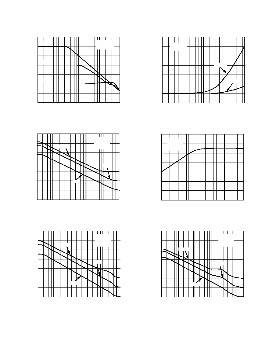
120
0
200
60
20
160
40
200
100
80
160
80
40
0
120
40
80
120
NUMBER OF UNITS
INPUT OFFSET VOLTAGE
µ
V
BASED ON 300 UNITS
3 RUNS
T
A
= +25
°
C
V
S
= +5V
V
CM
= 2.5V
Figure 16. Input Offset (V
IOS
) Distribution @ +5 V
120
0
2.50
60
20
0.25
40
0
100
80
2.25
1.75
1.50
1.25
2.00
1.00
0.75
0.50
NUMBER OF UNITS
TCV
IOS
µ
V/
°
C
300 UNITS
V
S
= +5V
V
CM
= 2.5V
Figure 18. Input Offset Drift (TCV
IOS
) Distribution @ +5 V
120
0
2.0
60
20
1.6
40
2.0
100
80
1.6
0.8
0.4
0
1.2
0.4
0.8
1.2
NUMBER OF UNITS
OUTPUT OFFSET mV
BASED ON 300 UNITS
3 RUNS
T
A
= +25
°
C
V
S
= +5V
V
CM
= 2.5V
Figure 20. Output Offset (V
OOS
) Distribution @ +5 V
120
0
0.5
60
20
0.4
40
0.5
100
80
0.4
0.2
0.1
0
0.3
0.1
0.2
0.3
NUMBER OF UNITS
INPUT OFFSET VOLTAGE mV
BASED ON 300 UNITS
3 RUNS
T
A
= +25
°
C
V
S
=
±
15V
V
CM
= 0V
Figure 17. Input Offset (V
IOS
) Distribution @
±
15 V
120
0
2.50
60
20
0.25
40
0
100
80
2.25
1.75
1.50
1.25
2.00
1.00
0.75
0.50
NUMBER OF UNITS
300 UNITS
V
S
=
±
15V
V
CM
= 0V
TCV
IOS
µ
V/
°
C
Figure 19. Input Offset Drift (TCV
IOS
) Distribution @
±
15 V
120
0
5
60
20
4
40
5
100
80
4
2
1
0
3
1
2
3
NUMBER OF UNITS
OUTPUT OFFSET mV
BASED ON 300 UNITS
3 RUNS
T
A
= +25
°
C
V
S
=
±
15V
V
CM
= 0V
Figure 21. Output Offset (V
OOS
) Distribution @
±
15 V
AMP04
REV. A
13
120
0
20
60
20
2
40
0
100
80
18
14
12
10
16
8
6
4
NUMBER OF UNITS
TCV
OOS
µ
V/
°
C
300 UNITS
V
S
= +5V
V
CM
= 0V
Figure 22. Output Offset Drift (TCV
OOS
) Distribution
@ +5 V
TEMPERATURE
°
C
5.0
3.8
100
4.4
4.0
25
4.2
50
4.8
4.6
75
50
25
0
R
L
= 100k
V
S
= +5V
OUTPUT VOLTAGE SWING Volts
R
L
= 10k
R
L
= 2k
Figure 24. Output Voltage Swing vs. Temperature
@ +5 V
TEMPERATURE
°
C
40
0
100
10
5
25
50
20
15
25
30
35
75
50
25
0
V
S
= +5V,
V
CM
= 2.5V
V
S
=
±
15V,
V
CM
= 0V
INPUT
BIAS CURRENT nA
V
S
=
±
15V
V
S
= +5V
Figure 26. Input Bias Current vs. Temperature
NUMBER OF UNITS
TCV
OOS
µ
V/
°
C
120
0
24
60
20
4
40
2
100
80
22
18
16
14
20
12
10
8
6
300 UNITS
V
S
=
±
15V
V
CM
= 0V
Figure 23. Output Offset Drift (TCV
OOS
) Distribution
@
±
15 V
TEMPERATURE
°
C
15.0
15.1
100
14.8
15.0
25
14.9
50
12.5
14.7
14.6
13.0
13.5
14.0
14.5
75
50
25
0
R
L
= 100k
OUTPUT SWING Volts
+OUTPUT SWING Volts
R
L
= 10k
R
L
= 2k
R
L
= 100k
R
L
= 10k
V
S
= +5V
R
L
= 10k
R
L
= 2k
R
L
= 100k
R
L
= 10k
R
L
= 2k
R
L
= 100k
Figure 25. Output Voltage Swing vs. Temperature
@ +15 V
TEMPERATURE
°
C
INPUT
OFFSET CURRENT nA
8
0
50
100
6
2
25
4
50
75
25
0
V
S
= +5V,
V
CM
= 2.5V
V
S
=
±
15V
,
V
CM
= 0V
V
S
=
±
15V
V
S
= +5V
Figure 27. Input Offset Current vs. Temperature
AMP04
REV. A
14
50
30
20
1k
1M
100k
10k
100
40
10
20
10
0
FREQUENCY Hz
VOLTAGE GAIN dB
T
A
= +25
°
C
V
S
=
±
15V
G = 100
G = 10
G = 1
Figure 28. Closed-Loop Voltage Gain vs. Frequency
120
100
20
1
10
100k
10k
1k
100
80
60
40
20
0
T
A
= +25
°
C
V
S
=
±
15V
V
CM
= 2V
P-P
FREQUENCY Hz
COMMON-MODE REJECTION dB
G = 100
G = 10
G = 1
Figure 30. Common-Mode Rejection vs. Frequency
140
120
0
10
100
1M
100k
10k
1k
100
80
60
40
20
T
A
= +25
°
C
V
S
=
±
15V
V
S
=
±
1V
FREQUENCY Hz
POWER SUPPLY REJECTION dB
G = 100
G = 10
G = 1
Figure 32. Positive Power Supply Rejection vs. Frequency
120
80
100
100k
10k
1k
10
100
40
60
0
20
FREQUENCY Hz
OUTPUT IMPEDANCE
T
A
= +25
°
C
G = 1
V
S
=
±
15V
V
S
= +5V
Figure 29. Closed-Loop Output Impedance vs. Frequency
COMMON-MODE REJECTION dB
120
70
50
1
10
1k
100
100
60
80
90
110
T
A
= +25
°
C
V
S
=
±
15V
V
CM
= 2V
P-P
VOLTAGE GAIN G
Figure 31. Common-Mode Rejection vs. Voltage Gain
140
120
0
10
100
1M
100k
10k
1k
100
80
60
40
20
T
A
= +25
°
C
V
S
=
±
15V
V
S
=
±
1V
FREQUENCY Hz
POWER SUPPLY REJECTION dB
G = 100
G = 10
G = 1
Figure 33. Negative Power Supply Rejection vs. Frequency
AMP04
REV. A
15
1k
100
1
1
10
1k
100
10
VOLTAGE GAIN G
T
A
= +25
°
C
V
S
=
±
15V
= 100Hz
VOLTAGE NOISE nV/ Hz
Figure 34. Voltage Noise Density vs. Gain
140
100
0
10
10k
1k
100
1
120
60
80
20
40
T
A
= +25
°
C
V
S
=
±
15V
G = 100
FREQUENCY Hz
VOLTAGE
NOISE
DENSITY
nV/ Hz
Figure 36. Voltage Noise Density vs. Frequency
1200
0
100
600
200
25
400
50
1000
800
75
50
25
0
TEMPERATURE
°
C
SUPPLY CURRENT
µ
A
V
S
= +5V
V
S
=
±
15V
Figure 38. Supply Current vs. Temperature
1k
100
1
1
10
1k
100
10
VOLTAGE GAIN G
T
A
= +25
°
C
V
S
=
±
15V
= 1kHz
VOLTAGE NOISE nV/ Hz
Figure 35. Voltage Noise Density vs. Gain, f = 1 kHz
10
90
100
0%
20mV
1s
V
S
=
±
15V, GAIN = 1000, 0.1 TO 10 Hz BANDPASS
Figure 37. Input Noise Voltage
16
8
0
100
100k
10k
1k
10
4
12
10
6
2
14
LOAD RESISTANCE
T
A
= +25
°
C
V
S
=
±
15V
OUTPUT VOLTAGE V
Figure 39. Maximum Output Voltage vs. Load Resistance
AMP04
REV. A
16
C17202410/92
PRINTED IN U.S.A.
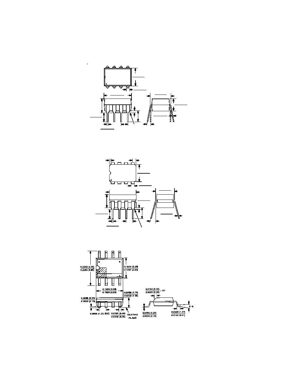
OUTLINE DIMENSIONS
Dimensions shown in inches and (mm).
8-Lead Plastic DIP (N-8)
0.160 (4.06)
0.115 (2.93)
0.130
(3.30)
MIN
0.210
(5.33)
MAX
0.015
(0.381) TYP
0.430 (10.92)
0.348 (8.84)
0.280 (7.11)
0.240 (6.10)
4
5
8
1
0.070 (1.77)
0.045 (1.15)
0.022 (0.558)
0.014 (0.356)
0.325 (8.25)
0.300 (7.62)
0
°
- 15
°
0.100
(2.54)
BSC
0.015 (0.381)
0.008 (0.204)
SEATING
PLANE
0.195 (4.95)
0.115 (2.93)
8-Lead Cerdip (Q-8)
0.005 (0.13) MIN
0.055 (1.4) MAX
0.405 (10.29) MAX
0.150
(3.81)
MIN
0.200
(5.08)
MAX
0.070 (1.78)
0.030 (0.76)
0.200 (5.08)
0.125 (3.18)
0.023 (0.58)
0.014 (0.36)
0.320 (8.13)
0.290 (7.37)
0
°
-15
°
0.015 (0.38)
0.008 (0.20)
0.100 (2.54)
BSC
SEATING PLANE
0.060 (1.52)
0.015 (0.38)
4
1
5
8
0.310 (7.87)
0.220 (5.59)
8-Lead Narrow-Body SO (S0-8)