Document Outline
- FEATURES
- APPLICATIONS
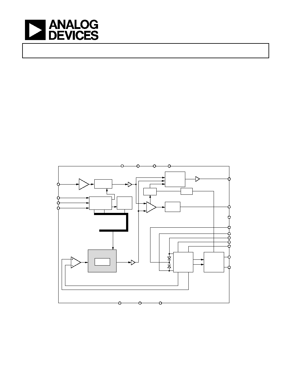
- FUNCTIONAL BLOCK DIAGRAM
- GENERAL DESCRIPTION
- TABLE OF CONTENTS
- ˛ˇ
- ˛ˇ
- ˛ˇ
- ˛ˇ
- ˛ˇ
- ˛ˇ
- ˛ˇ
Integrated Synthesizer and VCO
ADF4360-8
Rev. 0
Information furnished by Analog Devices is believed to be accurate and reliable.
However, no responsibility is assumed by Analog Devices for its use, nor for any
infringements of patents or other rights of third parties that may result from its use.
Specifications subject to change without notice. No license is granted by implication
or otherwise under any patent or patent rights of Analog Devices. Trademarks and
registered trademarks are the property of their respective owners.
One Technology Way, P.O. Box 9106, Norwood, MA 02062-9106, U.S.A.
Tel: 781.329.4700
www.analog.com
Fax: 781.326.8703
© 2004 Analog Devices, Inc. All rights reserved.
FEATURES
Output frequency range: 65 MHz to 400 MHz
3.0 V to 3.6 V power supply
1.8 V logic compatibility
Integer-N synthesizer
Programmable output power level
3-wire serial interface
Digital lock detect
Hardware and software power-down mode
APPLICATIONS
System clock generation
Test equipment
Wireless LANs
CATV equipment
GENERAL DESCRIPTION
The ADF4360-8 is an integrated integer-N synthesizer and
voltage controlled oscillator (VCO). The ADF4360-8 center
frequency is set by external inductors. This allows a frequency
range of between 65 MHz to 400 MHz.
Control of all the on-chip registers is through a simple 3-wire
interface. The device operates with a power supply ranging from
3.0 V to 3.6 V and can be powered down when not in use.
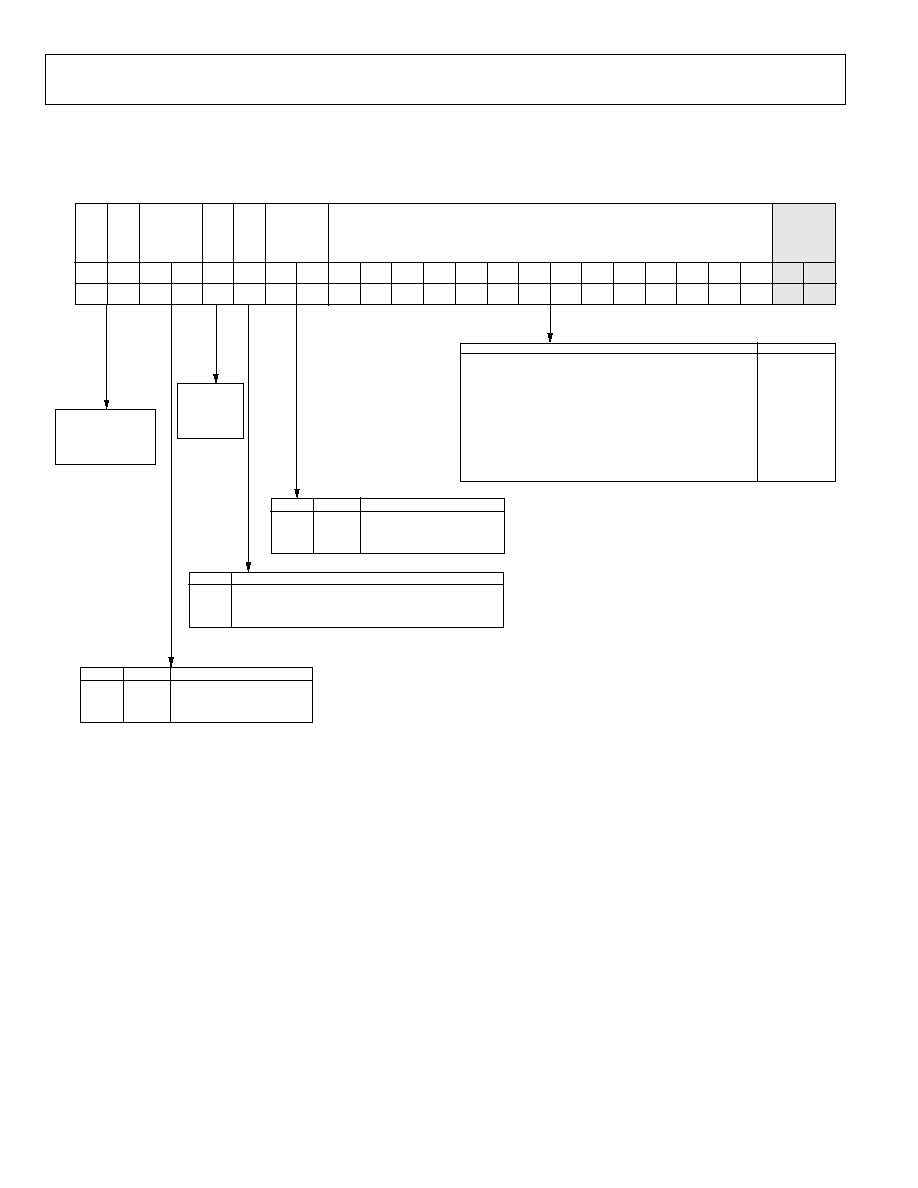
FUNCTIONAL BLOCK DIAGRAM
MUXOUT
CP
V
VCO
REF
IN
CLK
DATA
LE
AV
DD
DV
DD
CE
AGND
DGND
CPGND
R
SET
V
TUNE
C
C
C
N
L2
L1
RF
OUT
A
RF
OUT
B
VCO
CORE
PHASE
COMPARATOR
MUTE
N = B
CHARGE
PUMP
OUTPUT
STAGE
13-BIT B
COUNTER
14-BIT R
COUNTER
24-BIT
FUNCTION
LATCH
24-BIT
DATA REGISTER
MULTIPLEXER
LOCK
DETECT
ADF4360-8
04763-
001
Figure 1.

ADF4360-8
Rev. 0 | Page 2 of 24
TABLE OF CONTENTS
Specifications..................................................................................... 3
Timing Characteristics..................................................................... 5
Absolute Maximum Ratings............................................................ 6
Transistor Count........................................................................... 6
ESD Caution.................................................................................. 6
Pin Configuration and Function Descriptions............................. 7
Typical Performance Characteristics ............................................. 8
Circuit Description......................................................................... 10
Reference Input Section............................................................. 10
N Counter.................................................................................... 10
R Counter .................................................................................... 10
PFD and Charge Pump.............................................................. 10
MUXOUT and Lock Detect...................................................... 10
Input Shift Register..................................................................... 11
VCO ............................................................................................. 11
Output Stage................................................................................ 12
Latch Structure ........................................................................... 13
Control Latch .............................................................................. 17
N Counter Latch......................................................................... 18
R Counter Latch ......................................................................... 18
Choosing the Correct Inductance Value ................................. 19
Fixed Frequency LO................................................................... 19
Power-Up..................................................................................... 20
Interfacing ................................................................................... 20
PCB Design Guidelines for Chip Scale Package........................... 20
Output Matching ........................................................................ 21
Outline Dimensions ....................................................................... 22
Ordering Guide .......................................................................... 22
REVISION HISTORY
10/04--Revision 0: Initial Version

ADF4360-8
Rev. 0 | Page 3 of 24
SPECIFICATIONS
1
AV
DD
= DV
DD
= V
VCO
= 3.3 V ± 10%; AGND = DGND = 0 V; T
A
= T
MIN
to T
MAX
, unless otherwise noted.
Table 1.
Parameter B
Version
Unit
Conditions/Comments
REF
IN
CHARACTERISTICS
REF
IN
Input Frequency
10/250
MHz min/max
For f < 10 MHz, use a dc-coupled CMOS-compatible
square wave, slew rate > 21 V/µs.
REF
IN
Input Sensitivity
0.7/AV
DD
V p-p min/max
AC-coupled.
0 to AV
DD
V max
CMOS-compatible.
REF
IN
Input Capacitance
5.0
pF max
REF
IN
Input Current
±60
µA max
PHASE DETECTOR
Phase Detector Frequency
2
8
MHz max
CHARGE PUMP
I
CP
Sink/Source
3
With R
SET
= 4.7 k.
High Value
2.5
mA typ
Low Value
0.312
mA typ
R
SET
Range
2.7/10
k
I
CP
Three-State Leakage Current
0.2
nA typ
Sink and Source Current Matching
2
% typ
1.25 V V
CP
2.5 V.
I
CP
vs. V
CP
1.5
% typ
1.25 V V
CP
2.5 V.
I
CP
vs. Temperature
2
% typ
V
CP
= 2.0 V.
LOGIC INPUTS
V
INH
, Input High Voltage
1.5
V min
V
INL
, Input Low Voltage
0.6
V max
I
INH
/I
INL
, Input Current
±1
µA max
C
IN
, Input Capacitance
3.0
pF max
LOGIC OUTPUTS
V
OH
, Output High Voltage
DV
DD
≠ 0.4 V min
CMOS output chosen.
I
OH
, Output High Current
500
µA max
V
OL
, Output Low Voltage
0.4
V max
I
OL
= 500 µA.
POWER SUPPLIES
AV
DD
3.0/3.6
V min/V max
DV
DD
AV
DD
V
VCO
AV
DD
AI
DD
4
5
mA
typ
DI
DD
4
2.5
mA typ
I
VCO
4, 5
12.0
mA typ
I
CORE
= 5 mA.
I
RFOUT
4
3.5 to 11.0
mA typ
RF output stage is programmable.
Low Power Sleep Mode
4
7
µA typ
Specifications continued on next page.
Footnotes on next page.

ADF4360-8
Rev. 0 | Page 4 of 24
Parameter B
Version
Unit
Conditions/Comments
RF OUTPUT CHARACTERISTICS
5
Maximum VCO Output Frequency
400
MHz
I
CORE
= 5 mA. Depending on L. See the
Choosing the Correct Inductance Value section.
Minimum VCO Output Frequency
65
MHz
VCO Output Frequency
88/108
MHz min/max
L1, L2 = 270 nH. See the Choosing the Correct Inductance Value
section for other frequency values.
VCO Frequency Range
1.2
Ratio
F
MAX
/ F
MIN
VCO Sensitivity
2
MHz/V typ
L1, L2 = 270 nH. See the Choosing the Correct Inductance Value
section for other sensitivity values.
Lock Time
6
400
µs typ
To within 10 Hz of final frequency.
Frequency Pushing (Open Loop)
0.24
MHz/V typ
Frequency Pulling (Open Loop)
10
Hz typ
Into 2.00 VSWR load.
Harmonic Content (Second)
-16
dBc typ
Harmonic Content (Third)
-21
dBc typ
Output Power
5, 7
-9/0
dBm typ
Using tuned load, programmable in 3 dB steps. See Table 7.
Output Power
5, 8
-14/-9
dBm typ
Using 50 resistors to V
VCO
, programmable in 3 dB steps. See Table 7.
Output Power Variation
±3
dB typ
VCO Tuning Range
1.25/2.5
V min/max
NOISE CHARACTERISTICS
5
VCO Phase Noise Performance
9
-120
dBc/Hz typ
@ 100 kHz offset from carrier.
-139
dBc/Hz typ
@ 800 kHz offset from carrier.
-140
dBc/Hz typ
@ 3 MHz offset from carrier.
-142
dBc/Hz typ
@ 10 MHz offset from carrier.
Synthesizer Phase Noise Floor
10
-160
dBc/Hz typ
@ 200 kHz PFD frequency.
-150
dBc/Hz typ
@ 1 MHz PFD frequency.
-142
dBc/Hz typ
@ 8 MHz PFD frequency.
Phase Noise Figure of Merit
10
-209 dBc/Hz
typ
In-Band Phase Noise
11, 12
-102
dBc/Hz typ
@ 1 kHz offset from carrier.
RMS Integrated Phase Error
13
0.09
Degrees typ
100 Hz to 100 kHz.
Spurious Signals due to PFD
Frequency
12,
14
-75 dBc
typ
Level of Unlocked Signal with
MTLD Enabled
-70 dBm
typ
1
Operating temperature range is ≠40∞C to +85∞C.
2
Guaranteed by design. Sample tested to ensure compliance.
3
I
CP
is internally modified to maintain constant loop gain over the frequency range.
4
T
A
= 25∞C; AV
DD
= DV
DD
= V
VCO
= 3.3 V.
5
Unless otherwise stated, these characteristics are guaranteed for VCO core power = 5 mA. L1, L2 = 270 nH, 470 resistors to GND in parallel with L1, L2.
6
Jumping from 88 MHz to 108 MHz. PFD frequency = 200 kHz; loop bandwidth = 10 kHz.
7
For more detail on using tuned loads, see Output Matching section.
8
Using 50 resistors to V
VCO
, into a 50 load.
9
The noise of the VCO is measured in open-loop conditions.
10
The synthesizer phase noise floor is estimated by measuring the in-band phase noise at the output of the VCO and subtracting 20 log N (where N is the N divider value). The
phase noise figure of merit subtracts 10 log (PFD frequency).
11
The phase noise is measured with the EVAL-ADF4360-xEB1 Evaluation Board and the HP 8562E Spectrum Analyzer. The Spectrum Analyzer provides the REFIN for the
synthesizer; offset frequency = 1 kHz.
12
f
REFIN
= 10 MHz; f
PFD
= 200 kHz; N = 1000; Loop B/W = 10 kHz.
13
f
REFIN
= 10 MHz; f
PFD
= 1 MHz; N = 120; Loop B/W = 100 kHz.
14
The spurious signals are measured with the EVAL-ADF4360-xEB1 Evaluation Board and the HP 8562E Spectrum Analyzer. The Spectrum Analyzer provides the REFIN
for the synthesizer; f
REFOUT
= 10 MHz @ 0 dBm.
ADF4360-8
Rev. 0 | Page 5 of 24
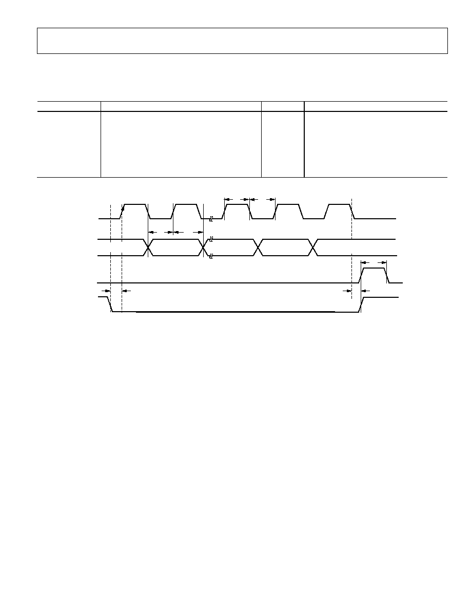
TIMING CHARACTERISTICS
AV
DD
= DV
DD
= V
VCO
= 3.3 V ± 10%; AGND = DGND = 0 V; 1.8 V and 3 V logic levels used; T
A
= T
MIN
to T
MAX
, unless otherwise noted.
Table 2.
Parameter
Limit at T
MIN
to T
MAX
(B Version)
Unit
Test Conditions/Comments
t
1
20
ns min
LE Setup Time
t
2
10
ns min
DATA to CLOCK Setup Time
t
3
10
ns min
DATA to CLOCK Hold Time
t
4
25
ns min
CLOCK High Duration
t
5
25
ns min
CLOCK Low Duration
t
6
10
ns min
CLOCK to LE Setup Time
t
7
20
ns min
LE Pulse Width
CLOCK
DATA
LE
LE
DB23 (MSB)
DB22
DB2
DB1
(CONTROL BIT C2)
DB0 (LSB)
(CONTROL BIT C1)
t
1
t
2
t
3
t
7
t
6
t
4
t
5
04763-002
Figure 2. Timing Diagram
ADF4360-8
Rev. 0 | Page 6 of 24
ABSOLUTE MAXIMUM RATINGS
T
A
= 25∞C, unless otherwise noted.
Table 3.
Parameter Rating
AV
DD
to GND
1
-0.3 V to +3.9 V
AV
DD
to DV
DD
-0.3 V to +0.3 V
V
VCO
to GND
-0.3 V to +3.9 V
V
VCO
to AV
DD
-0.3 V to +0.3 V
Digital I/O Voltage to GND
-0.3 V to V
DD
+ 0.3 V
Analog I/O Voltage to GND
-0.3 V to V
DD
+ 0.3 V
REF
IN
to GND
-0.3 V to V
DD
+ 0.3 V
Operating Temperature Range
-40∞C to + 85∞C
Storage Temperature Range
-65∞C to +150∞C
Maximum Junction Temperature
150∞C
CSP
JA
Thermal Impedance
Paddle Soldered
50∞C/W
Paddle Not Soldered
88∞C/W
Lead Temperature, Soldering
Vapor Phase (60 sec)
215∞C
Infrared (15 sec)
220∞C
1
GND = AGND = DGND = 0 V.
Stresses above those listed under Absolute Maximum Ratings
may cause permanent damage to the device. This is a stress
rating only; functional operation of the device at these or any
other conditions above those listed in the operational sections
of this specification is not implied. Exposure to absolute maxi-
mum rating conditions for extended periods may affect device
reliability.
This device is a high performance RF integrated circuit with an
ESD rating of <1 kV, and it is ESD sensitive. Proper precautions
should be taken for handling and assembly.
TRANSISTOR COUNT
12543 (CMOS) and 700 (Bipolar)
ESD CAUTION
ESD (electrostatic discharge) sensitive device. Electrostatic charges as high as 4000 V readily accumulate on the
human body and test equipment and can discharge without detection. Although this product features proprie-
tary ESD protection circuitry, permanent damage may occur on devices subjected to high energy electrostatic
discharges. Therefore, proper ESD precautions are recommended to avoid performance degradation or loss of
functionality.
ADF4360-8
Rev. 0 | Page 7 of 24
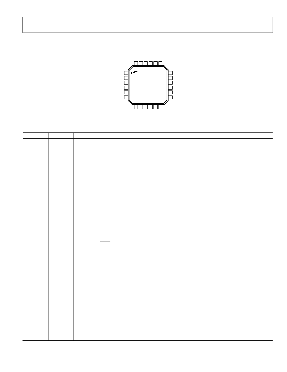
PIN CONFIGURATION AND FUNCTION DESCRIPTIONS
ADF4360-8
TOP VIEW
(Not to Scale)
CPGND
1
AV
DD
2
AGND
3
RF
OUT
A
4
RF
OUT
B
5
V
VCO
6
DATA
18
CLK
17
REF
IN
16
DGND
15
C
N
14
R
SET
13
V
TUNE
7
AGND
8
L1
9
L2
10
AGND
11
C
C
12
CP
24
CE
23
AGND
22
DV
DD
21
MUX
O
U
T
20
LE
19
04763-003
PIN 1
IDENTIFIER
Figure 3. Pin Configuration
Table 4. Pin Function Descriptions
Pin No.
Mnemonic
Function
1
CPGND
Charge Pump Ground. This is the ground return path for the charge pump.
2 AV
DD
Analog Power Supply. This ranges from 3.0 V to 3.6 V. Decoupling capacitors to the analog ground plane should be
placed as close as possible to this pin. AV
DD
must have the same value as DV
DD
.
3, 8, 11, 22
AGND
Analog Ground. This is the ground return path of the prescaler and VCO.
4 RF
OUT
A
VCO Output. The output level is programmable from 0 dBm to
-9 dBm. See the Output Matching section for a
description of the various output stages.
5 RF
OUT
B
VCO Complementary Output. The output level is programmable from 0 dBm to -9 dBm. See the Output Matching
section for a description of the various output stages.
6 V
VCO
Power Supply for the VCO. This ranges from 3.0 V to 3.6 V. Decoupling capacitors to the analog ground plane should
be placed as close as possible to this pin. V
VCO
must have the same value as AV
DD
.
7 V
TUNE
Control Input to the VCO. This voltage determines the output frequency and is derived from filtering the CP
output voltage.
9
L1
An external inductor to AGND should be connected to this pin to set the ADF4360-8 output frequency. L1 and L2
need to be the same value. A 470 resistor should be added in parallel to AGND.
10 L2
An external inductor to AGND should be connected to this pin to set the ADF4360-8 output frequency. L1 and L2
need to be the same value. A 470 resistor should be added in parallel to AGND.
12 C
C
Internal Compensation Node. This pin must be decoupled to ground with a 10 nF capacitor.
13 R
SET
Connecting a resistor between this pin and CP
GND
sets the maximum charge pump output current for the synthesizer.
The nominal voltage potential at the R
SET
pin is 0.6 V. The relationship between I
CP
and R
SET
is
SET
CPmax
R
I
75
.
11
=
where R
SET
= 4.7 k, I
CPmax
= 2.5 mA.
14 C
N
Internal Compensation Node. This pin must be decoupled to V
VCO
with a 10 µF capacitor.
15
DGND
Digital Ground.
16 REF
IN
Reference Input. This is a CMOS input with a nominal threshold of V
DD
/2 and a dc equivalent input resistance of
100 k (see Figure 16). This input can be driven from a TTL or CMOS crystal oscillator, or it can be ac-coupled.
17
CLK
Serial Clock Input. This serial clock is used to clock in the serial data to the registers. The data is latched into the 24-bit
shift register on the CLK rising edge. This input is a high impedance CMOS input.
18
DATA
Serial Data Input. The serial data is loaded MSB first with the two LSBs being the control bits. This input is a high
impedance CMOS input.
19
LE
Load Enable, CMOS Input. When LE goes high, the data stored in the shift registers is loaded into one of the four
latches, and the relevant latch is selected using the control bits.
20
MUXOUT
This multiplexer output allows either the lock detect, the scaled RF, or the scaled reference frequency to be
accessed externally.
21 DV
DD
Digital Power Supply. This ranges from 3.0 V to 3.6 V. Decoupling capacitors to the digital ground plane should be
placed as close as possible to this pin. DV
DD
must have the same value as AV
DD
.
23
CE
Chip Enable. A logic low on this pin powers down the device and puts the charge pump into three-state mode.
Taking the pin high powers up the device depending on the status of the power-down bits.
24
CP
Charge Pump Output. When enabled, this provides ± I
CP
to the external loop filter, which in turn drives the internal VCO.
ADF4360-8
Rev. 0 | Page 8 of 24
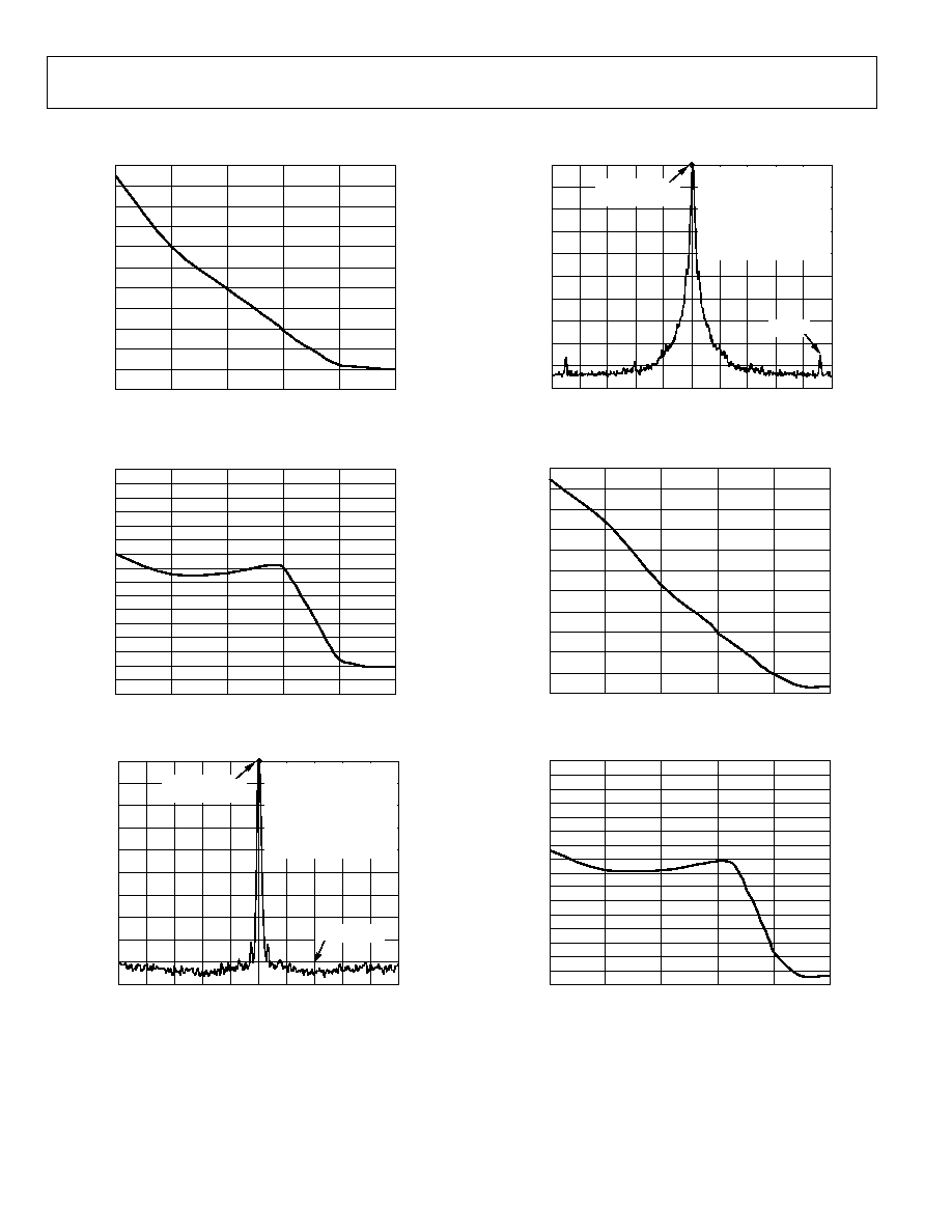
TYPICAL PERFORMANCE CHARACTERISTICS
≠150
≠120
≠130
≠140
≠70
≠60
≠90
≠100
≠110
≠80
≠40
≠50
100
1k
10k
100k
1M
10M
FREQUENCY OFFSET (Hz)
OUTP
UT P
O
W
E
R (dB)
04763-004
Figure 4. Open-Loop VCO Phase Noise, L1, L2 = 560 nH
≠150
≠125
≠130
≠120
≠135
≠140
≠145
≠85
≠80
≠95
≠100
≠105
≠110
≠115
≠90
≠70
≠75
100
1k
10k
100k
1M
10M
FREQUENCY OFFSET (Hz)
OUTP
UT P
O
W
E
R (dB)
04763-005
Figure 5. VCO Phase Noise, 65 MHz, 1 MHz PFD, 100 kHz Loop Bandwidth
04763-006
OUTP
UT P
O
W
E
R (dB)
≠90
≠80
≠70
≠60
≠50
≠40
≠30
≠20
≠10
0
≠2kHz
≠1kHz
65MHz
1kHz
2kHz
≠107.4dBc/Hz
REFERENCE
LEVEL = ≠2.5dBm
V
DD
= 3.3V, V
VCO
= 3.3V
I
CP
= 2.5mA
PFD FREQUENCY = 1MHz
LOOP BANDWIDTH = 100kHz
RES. BANDWIDTH = 30Hz
VIDEO BANDWIDTH = 30Hz
SWEEP = 1.9SECONDS
AVERAGES = 20
Figure 6. Close-In Phase Noise at 65 MHz (1 MHz Channel Spacing)
04763-007
OUTP
UT P
O
W
E
R (dB)
≠90
≠80
≠70
≠60
≠50
≠40
≠30
≠20
≠10
0
≠1.1MHz
≠0.55MHz
65MHz
0.55MHz
1.1MHz
≠84dBc
REFERENCE
LEVEL = ≠2.5dBm
V
DD
= 3.3V, V
VCO
= 3.3V
I
CP
= 2.5mA
PFD FREQUENCY = 1MHz
LOOP BANDWIDTH = 100kHz
RES. BANDWIDTH = 1kHz
VIDEO BANDWIDTH = 1kHz
SWEEP = 4.2SECONDS
AVERAGES = 20
Figure 7. Reference Spurs at 65 MHz
(1 MHz Channel Spacing, 100 kHz Loop Bandwidth)
≠150
≠120
≠130
≠140
≠70
≠60
≠90
≠100
≠110
≠80
≠40
≠50
100
1k
10k
100k
1M
10M
FREQUENCY OFFSET (Hz)
OUTP
UT P
O
W
E
R (dB)
04763-008
Figure 8. Open-Loop VCO Phase Noise, L1, L2 = 110 nH
≠150
≠125
≠130
≠120
≠135
≠140
≠145
≠85
≠80
≠95
≠100
≠105
≠110
≠115
≠90
≠70
≠75
100
1k
10k
100k
1M
10M
FREQUENCY OFFSET (Hz)
OUTP
UT P
O
W
E
R (dB)
04763-009
Figure 9. VCO Phase Noise, 160 MHz, 1 MHz PFD, 100 kHz Loop Bandwidth
ADF4360-8
Rev. 0 | Page 9 of 24
04763-010
OUTP
UT P
O
W
E
R (dB)
≠90
≠80
≠70
≠60
≠50
≠40
≠30
≠20
≠10
0
≠2kHz
≠1kHz
160MHz
1kHz
2kHz
≠109.4dBc/Hz
REFERENCE
LEVEL = 1dBm
V
DD
= 3.3V, V
VCO
= 3.3V
I
CP
= 2.5mA
PFD FREQUENCY = 1MHz
LOOP BANDWIDTH = 100kHz
RES. BANDWIDTH = 30Hz
VIDEO BANDWIDTH = 30Hz
SWEEP = 1.9SECONDS
AVERAGES = 20
Figure 10. Close-In Phase Noise at 160 MHz (1 MHz Channel Spacing)
04763-011
OUTP
UT P
O
W
E
R (dB)
≠90
≠80
≠70
≠60
≠50
≠40
≠30
≠20
≠10
0
≠1.1MHz
≠0.55MHz
160MHz
0.55MHz
1.1MHz
≠76dBc
REFERENCE
LEVEL = 1dBm
V
DD
= 3.3V, V
VCO
= 3.3V
I
CP
= 2.5mA
PFD FREQUENCY = 1MHz
LOOP BANDWIDTH = 100kHz
RES. BANDWIDTH = 1kHz
VIDEO BANDWIDTH = 1kHz
SWEEP = 4.2SECONDS
AVERAGES = 20
Figure 11. Reference Spurs at 160 MHz
(1 MHz Channel Spacing, 100 kHz Loop Bandwidth)
≠150
≠120
≠130
≠140
≠70
≠60
≠90
≠100
≠110
≠80
≠40
≠50
100
1k
10k
100k
1M
10M
FREQUENCY OFFSET (Hz)
OUTP
UT P
O
W
E
R (dB)
04763-012
Figure 12. Open-Loop VCO Phase Noise, L1, L2 = 18 nH
≠150
≠125
≠130
≠120
≠135
≠140
≠145
≠85
≠80
≠95
≠100
≠105
≠110
≠115
≠90
≠70
≠75
100
1k
10k
100k
1M
10M
FREQUENCY OFFSET (Hz)
OUTP
UT P
O
W
E
R (dB)
04763-013
Figure 13. VCO Phase Noise, 400 MHz, 1 MHz PFD, 100 kHz Loop Bandwidth
04763-014
OUTP
UT P
O
W
E
R (dB)
≠90
≠80
≠70
≠60
≠50
≠40
≠30
≠20
≠10
0
≠2kHz
≠1kHz
400MHz
1kHz
2kHz
≠103.4dBc/Hz
REFERENCE
LEVEL = 0dBm
V
DD
= 3.3V, V
VCO
= 3.3V
I
CP
= 2.5mA
PFD FREQUENCY = 1MHz
LOOP BANDWIDTH = 100kHz
RES. BANDWIDTH = 30Hz
VIDEO BANDWIDTH = 30Hz
SWEEP = 1.9SECONDS
AVERAGES = 20
Figure 14. Close-In Phase Noise at 400 MHz (1 MHz Channel Spacing)
04763-015
OUTP
UT P
O
W
E
R (dB)
≠90
≠80
≠70
≠60
≠50
≠40
≠30
≠20
≠10
0
≠1.1MHz
≠0.55MHz
400MHz
0.55MHz
1.1MHz
≠77dBc
REFERENCE
LEVEL = 0dBm
V
DD
= 3.3V, V
VCO
= 3.3V
I
CP
= 2.5mA
PFD FREQUENCY = 1MHz
LOOP BANDWIDTH = 100kHz
RES. BANDWIDTH = 1kHz
VIDEO BANDWIDTH = 1kHz
SWEEP = 4.2SECONDS
AVERAGES = 20
Figure 15. Reference Spurs at 400 MHz
(1 MHz Channel Spacing, 100 kHz Loop Bandwidth)
ADF4360-8
Rev. 0 | Page 10 of 24
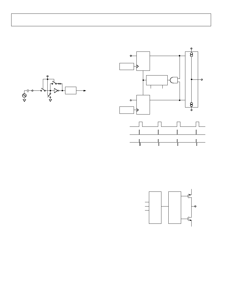
CIRCUIT DESCRIPTION
REFERENCE INPUT SECTION
The reference input stage is shown in Figure 16. SW1 and SW2
are normally closed switches. SW3 is normally open. When
power-down is initiated, SW3 is closed, and SW1 and SW2 are
opened. This ensures that there is no loading of the REF
IN
pin
on power-down.
04763-016
BUFFER
TO R COUNTER
REF
IN
100k
NC
SW2
SW3
NO
NC
SW1
POWER-DOWN
CONTROL
Figure 16. Reference Input Stage
N COUNTER
The CMOS N counter allows a wide division ratio in the PLL
feedback counter. The counters are specified to work when
the VCO output is 400 MHz or less. To avoid confusion, this is
referred to as the B counter. It makes it possible to generate
output frequencies that are spaced only by the reference
frequency divided by R. The VCO frequency equation is
R
f
B
f
REFIN
VCO
/
◊
=
where:
f
VCO
is the output frequency of the VCO. B is the preset divide
ratio of the binary 13-bit counter (3 to 8191).
f
REFIN
is the external reference frequency oscillator.
R COUNTER
The 14-bit R counter allows the input reference frequency to
be divided down to produce the reference clock to the phase
frequency detector (PFD). Division ratios from 1 to 16,383 are
allowed.
PFD AND CHARGE PUMP
The PFD takes inputs from the R counter and N counter (N =
BP
+ A) and produces an output proportional to the phase and
frequency difference between them. Figure 17 is a simplified
schematic. The PFD includes a programmable delay element
that controls the width of the antibacklash pulse. This pulse
ensures that there is no dead zone in the PFD transfer function
and minimizes phase noise and reference spurs. Two bits in the
R counter latch, ABP2 and ABP1, control the width of the pulse
(see Table 9).
04763-
017
PROGRAMMABLE
DELAY
U3
CLR2
Q2
D2
U2
CLR1
Q1
D1
CHARGE
PUMP
DOWN
UP
HI
HI
U1
ABP1
ABP2
R DIVIDER
N DIVIDER
CP OUTPUT
R DIVIDER
N DIVIDER
CP
CPGND
V
P
Figure 17. PFD Simplified Schematic and Timing (In Lock)
MUXOUT AND LOCK DETECT
The output multiplexer on the ADF4360 family allows the user
to access various internal points on the chip. The state of
MUXOUT is controlled by M3, M2, and M1 in the function
latch. The full truth table is shown in Table 7. Figure 18 shows
the MUXOUT section in block diagram form.
R COUNTER OUTPUT
N COUNTER OUTPUT
DIGITAL LOCK DETECT
DGND
CONTROL
MUX
MUXOUT
DV
DD
04763-018
Figure 18. MUXOUT Circuit
ADF4360-8
Rev. 0 | Page 11 of 24
Lock Detect
The correct band is chosen automatically by the band select
logic at power-up or whenever the N counter latch is updated. It
is important that the correct write sequence be followed at
power-up. This sequence is
MUXOUT can be programmed for one type of lock detect.
Digital lock detect is active high. When LDP in the R counter
latch is set to 0, digital lock detect is set high when the phase error
on three consecutive phase detector cycles is less than 15 ns.
1.
R counter latch
With LDP set to 1, five consecutive cycles of less than 15 ns
phase error are required to set the lock detect. It stays set high
until a phase error of greater than 25 ns is detected on any
subsequent PD cycle.
2.
Control latch
3.
N counter latch
During band select, which takes five PFD cycles, the VCO V
TUNE
is disconnected from the output of the loop filter and connected
to an internal reference voltage.
INPUT SHIFT REGISTER
The ADF4360 family's digital section includes a 24-bit input
shift register, a 14-bit R counter, and an 18-bit N counter
comprised of a 5-bit A counter and a 13-bit B counter. Data is
clocked into the 24-bit shift register on each rising edge of CLK.
The data is clocked in MSB first. Data is transferred from the
shift register to one of four latches on the rising edge of LE. The
destination latch is determined by the state of the two control
bits (C2, C1) in the shift register. These are the two LSBs, DB1
and DB0, shown in Figure 2.
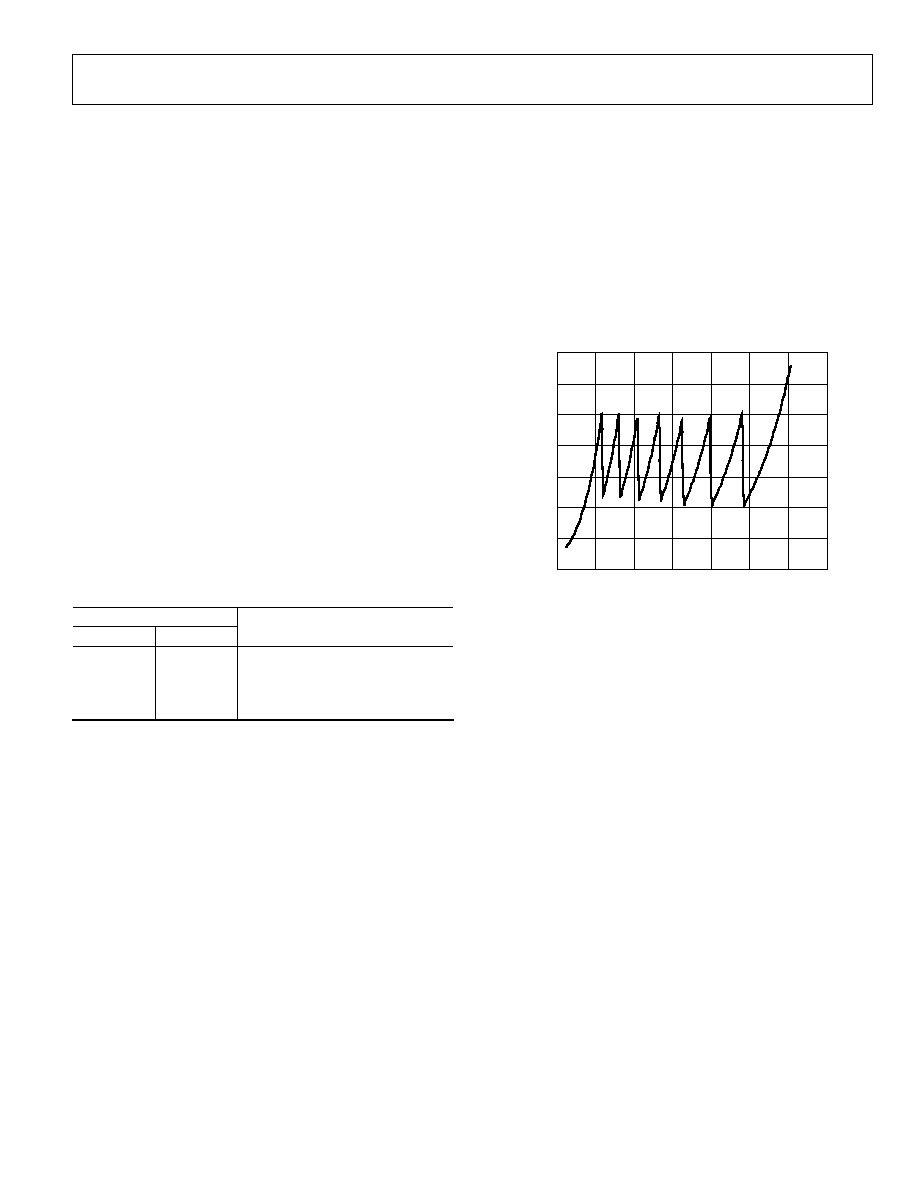
0
1.0
0.5
2.5
2.0
1.5
3.5
3.0
80
85
90
100
95
105
115
110
FREQUENCY (MHz)
V
TUNE
(V
)
04763-019
The truth table for these bits is shown in Table 5. Table 6 shows
a summary of how the latches are programmed. Note that the
test modes latch is used for factory testing and should not be
programmed by the user.
Table 5. C2 and C1 Truth Table
Figure 19. Frequency vs. V
TUNE
, ADF4360-8, L1 and L2 = 270 nH
Control Bits
C2
C1
Data Latch
0
0
Control Latch
0
1
R Counter
1
0
N Counter (B)
1
1
Test Modes Latch
The R counter output is used as the clock for the band select
logic and should not exceed 1 MHz. A programmable divider is
provided at the R counter input to allow division by 1, 2, 4, or 8
and is controlled by Bits BSC1 and BSC2 in the R counter latch.
Where the required PFD frequency exceeds 1 MHz, the divide
ratio should be set to allow enough time for correct band
selection.
VCO
The VCO core in the ADF4360 family uses eight overlapping
bands, as shown in Figure 19, to allow a wide frequency range to
be covered without a large VCO sensitivity (K
V
) and resultant
poor phase noise and spurious performance.
After band selection, normal PLL action resumes. The value of
K
V
is determined by the value of inductors used (see the
Choosing the Correct Inductance Value section). The ADF4360
family contains linearization circuitry to minimize any variation
of the product of I
CP
and K
V
.
The operating current in the VCO core is programmable in four
steps: 2.5 mA, 5 mA, 7.5 mA, and 10 mA. This is controlled by
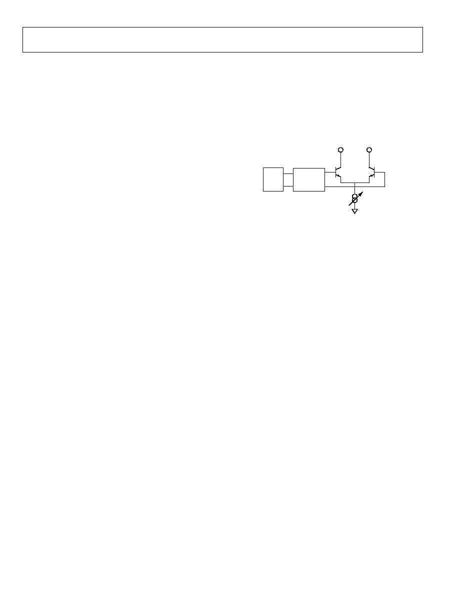
Bits PC1 and PC2 in the control latch.
ADF4360-8
Rev. 0 | Page 12 of 24
OUTPUT STAGE
The RF
OUT
A and RF
OUT
B pins of the ADF4360 family are
connected to the collectors of an NPN differential pair driven
by buffered outputs of the VCO, as shown in Figure 20. To allow
the user to optimize the power dissipation versus the output
power requirements, the tail current of the differential pair is
programmable via Bits PL1 and PL2 in the control latch. Four
current levels may be set: 3.5 mA, 5 mA, 7.5 mA, and 11 mA.
These levels give output power levels of -9 dBm, -6 dBm,
-3 dBm, and 0 dBm, respectively, using the correct shunt
inductor to V
DD
and ac coupling into a 50 load. Alternatively,
both outputs can be combined in a 1 + 1:1 transformer or a 180∞
microstrip coupler (see the Output Matching section).
If the outputs are used individually, the optimum output stage
consists of a shunt inductor to V
DD
.
Another feature of the ADF4360 family is that the supply current
to the RF output stage is shut down until the part achieves lock as
measured by the digital lock detect circuitry. This is enabled by the
Mute-Till-Lock Detect (MTLD) bit in the control latch.
VCO
RF
OUT
A
RF
OUT
B
BUFFER/
DIVIDE BY 2
04763-020
Figure 20. Output Stage ADF4360-8
ADF4360-8
Rev. 0 | Page 13 of 24
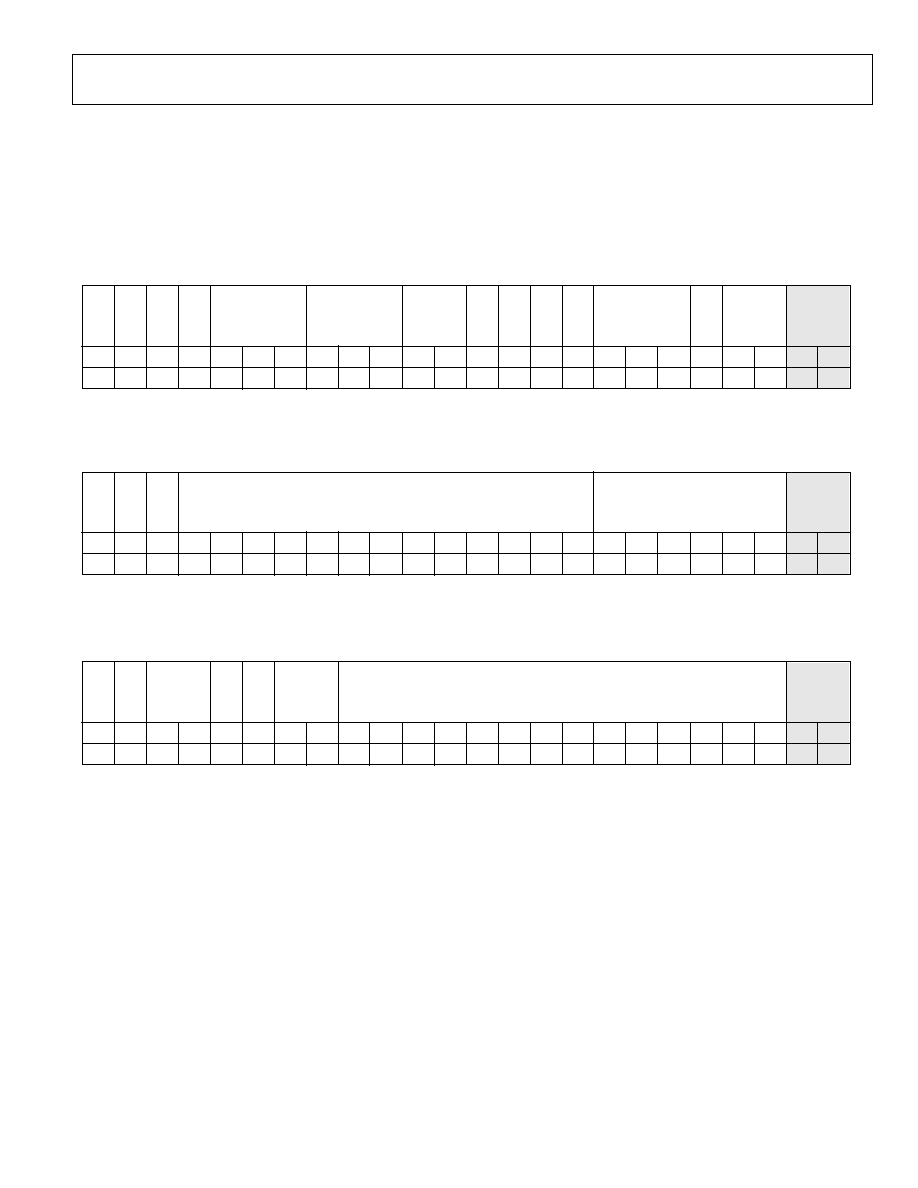
LATCH STRUCTURE
Table 6 shows the three on-chip latches for the ADF4360 family. The two LSBs decide which latch is programmed.
Table 6. Latch Structure
DB20 DB19 DB18 DB17 DB16 DB15 DB14 DB13 DB12 DB11 DB10 DB9 DB8
DB7
DB6
DB5
DB4
DB3
DB2
DB1
DB0
C2 (0) C1 (0)
PC1
PC2
CR
M1
M2
PDP
CP
CPG
MTLD
PL1
PL2
CPI1
CPI2
CPI3
CPI4
CPI5
CPI6
PD1
M3
CONTROL
BITS
MUXOUT
CONTROL
CURRENT
SETTING 2
CURRENT
SETTING 1
CORE
POWER
LEVEL
OUTPUT
POWER
LEVEL
DB21
DB22
DB23
POWER-
DOWN 2
RESERVED
RESERVED
RESERVED
RESERVED
POWER-
DOWN 1
COUNTER
RESET
MUTE-
T
IL-
LD
CP GAIN
CP
T
HREE-
ST
AT
E
PHASE
DET
E
CT
OR
POL
ARIT
Y
PD2
RSV
RSV
DB20 DB19 DB18 DB17 DB16 DB15 DB14 DB13 DB12 DB11 DB10 DB9 DB8
DB7
DB6
DB5
DB4
DB3
DB2
DB1
DB0
C2 (0) C1 (1)
R1
R2
R3
R4
R5
R7
R8
R9
R10
R11
R12
R13
R14
ABP1
ABP2
LDP
TMB
BSC1
R6
CONTROL
BITS
BAND
SELECT
CLOCK
ANTI-
BACKLASH
PULSE
WIDTH
14-BIT REFERENCE COUNTER
DB21
DB22
DB23
LOC
K
DET
E
CT
PRECISION
T
EST
MODE
BIT
RESERVED
RESERVED
BSC2
RSV
RSV
RSV
RSV
DB20 DB19 DB18 DB17 DB16 DB15 DB14 DB13 DB12 DB11 DB10 DB9 DB8
DB7
DB6
DB5
DB4
DB3
DB2
DB1
DB0
C2 (1) C1 (0)
RSV
RSV
RSV
RSV
RSV
B1
B2
B3
B4
B5
B6
B7
B8
B9
B10
B11
B12
B13
RSV
CONTROL
BITS
RESERVED
13-BIT B COUNTER
CONTROL LATCH
N COUNTER LATCH
R COUNTER LATCH
DB21
DB22
DB23
CP GAIN
CPG
04763-021
ADF4360-8
Rev. 0 | Page 14 of 24
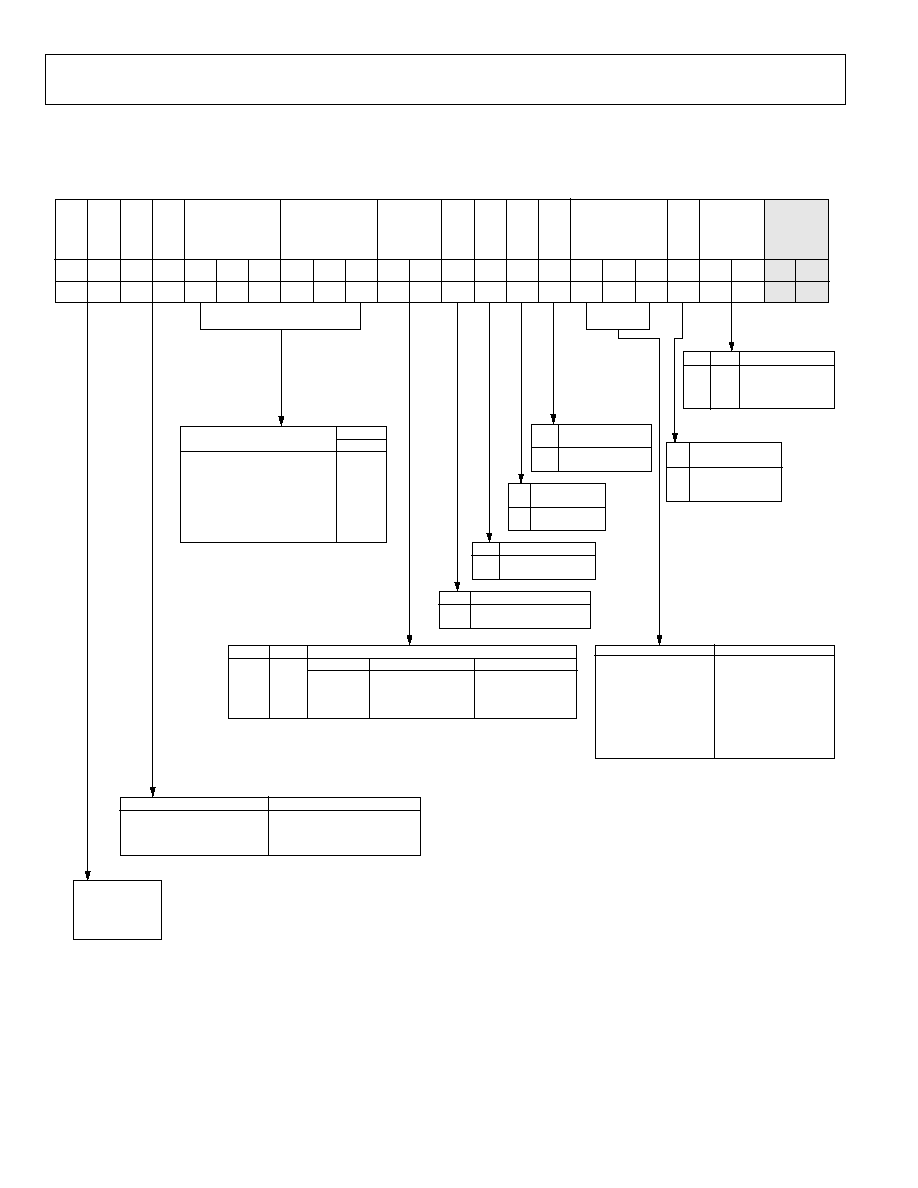
Table 7. Control Latch
DB20 DB19 DB18 DB17 DB16 DB15 DB14 DB13 DB12 DB11 DB10 DB9 DB8
DB7
DB6
DB5
DB4
DB3
DB2
DB1
DB0
C2 (0) C1 (0)
PC1
PC2
CR
M1
M2
PDP
CP
CPG
MTLD
PL1
PL2
CPI1
CPI2
CPI3
CPI4
CPI5
CPI6
PD1
M3
CONTROL
BITS
MUXOUT
CONTROL
CURRENT
SETTING 2
CURRENT
SETTING 1
CORE
POWER
LEVEL
OUTPUT
POWER
LEVEL
DB21
DB22
DB23
POWER-
DOWN 2
POWER-
DOWN 1
COUNT
ER
RESET
MUTE-TIL-
LD
RESERVED
RESERVED
CP GAIN
CP
THREE-
STATE
PHASE
DET
E
CT
O
R
PO
L
ARIT
Y
PD2
RSV
RSV
CR
0
1
COUNTER
OPERATION
NORMAL
R, A, B COUNTERS
HELD IN RESET
PC2
0
0
1
0
CORE POWER LEVEL
2.5mA
5mA
7.5mA
PC1
0
1
1
1
10mA
CP
0
1
CHARGE PUMP
OUTPUT
NORMAL
THREE-STATE
PDP
0
1
PHASE DETECTOR
POLARITY
NEGATIVE
POSITIVE
CPG
0
1
CP GAIN
CURRENT SETTING 1
CURRENT SETTING 2
MTLD
0
1
MUTE-TIL-LOCK DETECT
DISABLED
ENABLED
M3
M2
M1
MUXOUT
THREE-STATE OUTPUT
0
0
0
0
0
1
0
1
0
0
1
1
1
0
0
1
0
1
1
1
0
1
1
1
DIGITAL LOCK DETECT
(ACTIVE HIGH)
N DIVIDER OUTPUT
DV
DD
R DIVIDER OUTPUT
NOT USED
NOT USED
DGND
CE PIN
PD2
PD1
MODE
0
X
X
ASYNCHRONOUS POWER-DOWN
1
X
0
NORMAL OPERATION
1
0
1
ASYNCHRONOUS POWER-DOWN
1
1
1
SYNCHRONOUS POWER-DOWN
CPI6
CPI5
CPI4
I
CP
(mA)
CPI3
CPI2
CPI1
4.7k
0.31
0.62
0.93
1.25
1.56
1.87
2.18
2.50
0
0
0
0
1
1
1
1
0
0
1
1
0
0
1
1
0
1
0
1
0
1
0
1
PL2
PL1
OUTPUT POWER LEVEL
CURRENT
(USING TUNED LOAD)
≠9dBm
≠6dBm
≠3dBm
0dBm
(USING 50
TO V
VCO
)
≠19dBm
≠15dBm
≠12dBm
≠9dBm
0
0
1
1
0
1
0
1
3.5mA
5.0mA
7.5mA
11.0mA
04763-022
THESE BITS ARE
NOT USED BY THE
DEVICE AND ARE
DON'T CARE BITS.
ADF4360-8
Rev. 0 | Page 15 of 24
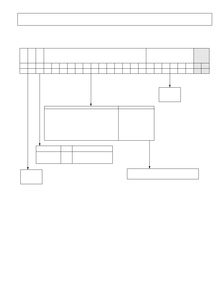
Table 8. N Counter Latch
DB20 DB19 DB18 DB17 DB16 DB15 DB14 DB13 DB12 DB11 DB10 DB9 DB8
DB7
DB6
DB5
DB4
DB3
DB2
DB1
DB0
C2 (1) C1 (0)
RSV
RSV
RSV
RSV
RSV
B1
B2
B3
B4
B5
B6
B7
B8
B9
B10
B11
B12
B13
RSV
CONTROL
BITS
RESERVED
13-BIT B COUNTER
DB21
DB22
DB23
CP G
A
IN
RESERVED
RESERVED
CPG
RSV
RSV
F4 (FUNCTION LATCH)
FASTLOCK ENABLE
CP GAIN
OPERATION
CHARGE PUMP CURRENT SETTING 1
IS PERMANENTLY USED
0
0
CHARGE PUMP CURRENT SETTING 2
IS PERMANENTLY USED
1
0
N = B; P IS PRESCALER VALUE SET IN THE CONTROL LATCH.
B MUST BE GREATER THAN OR EQUAL TO A. FOR CONTINUOUSLY
ADJACENT VALUES OF (N
◊
F
REF
), AT THE OUTPUT, N
MIN
IS (P
2
≠P).
B13
B12
B11
B3
B2
B1
B COUNTER DIVIDE RATIO
..........
0
0
0
0
0
0
0
0
0
0
0
0
0
0
0
NOT ALLOWED
..........
0
0
1
NOT ALLOWED
..........
0
1
0
NOT ALLOWED
..........
1
1
1
3
..........
.
.
.
.
.
.
.
.
.
.
.
.
.
..........
.
.
.
.
..........
.
.
.
.
..........
1
1
1
1
1
1
1
1
1
1
1
1
1
0
0
8188
..........
1
0
1
8189
..........
1
1
0
8190
..........
1
1
1
8191
04763-023
THESE BITS ARE
NOT USED BY THE
DEVICE AND ARE
DON'T CARE BITS.
THESE BITS ARE
NOT USED BY THE
DEVICE AND ARE
DON'T CARE BITS.
ADF4360-8
Rev. 0 | Page 16 of 24
Table 9. R Counter Latch
DB20 DB19 DB18 DB17 DB16 DB15 DB14 DB13 DB12 DB11 DB10 DB9 DB8
DB7
DB6
DB5
DB4
DB3
DB2
DB1
DB0
C2 (0) C1 (1)
R1
R2
R3
R4
R5
R7
R8
R9
R10
R11
R12
R13
R14
ABP1
ABP2
LDP
TMB
BSC1
R6
CONTROL
BITS
BAND
SELECT
CLOCK
ANTI-
BACKLASH
PULSE
WIDTH
14-BIT REFERENCE COUNTER
DB21
DB22
DB23
LO
CK
DETECT
PRECISION
TEST
MODE
BIT
RESERVED
RESERVED
BSC2
RSV
RSV
TEST MODE
BIT SHOULD
BE SET TO 0
FOR NORMAL
OPERATION.
R14
R13
R12
R3
R2
R1
DIVIDE RATIO
..........
0
0
0
0
0
0
0
0
0
0
0
0
0
0
1
1
..........
0
1
0
2
..........
0
1
1
3
..........
1
0
0
4
..........
.
.
.
.
.
.
.
.
.
.
.
.
.
..........
.
.
.
.
..........
.
.
.
.
..........
1
1
1
1
1
1
1
1
1
1
1
1
1
0
0
16380
..........
1
0
1
16381
..........
1
1
0
16382
..........
1
1
1
16383
THESE BITS ARE NOT
USED BY THE DEVICE
AND ARE DON'T CARE
BITS.
04763-
024
LDP
LOCK DETECT PRECISION
0
THREE CONSECUTIVE CYCLES OF PHASE DELAY LESS THAN
15ns MUST OCCUR BEFORE LOCK DETECT IS SET.
1
FIVE CONSECUTIVE CYCLES OF PHASE DELAY LESS THAN
15ns MUST OCCUR BEFORE LOCK DETECT IS SET.
ABP2
ABP1
ANTIBACKLASH PULSE WIDTH
0
0
3.0ns
0
1
1.3ns
1
0
6.0ns
1
1
3.0ns
BSC2
BSC1
BAND SELECT CLOCK DIVIDER
0
0
1
0
1
2
1
0
4
1
1
8

ADF4360-8
Rev. 0 | Page 17 of 24
CONTROL LATCH
With (C2, C1) = (0,0), the control latch is programmed. Table 7
shows the input data format for programming the control latch.
Power-Down
DB21 (PD2) and DB20 (PD1) provide programmable power-
down modes.
In the programmed asynchronous power-down, the device
powers down immediately after latching a 1 into Bit PD1,
with the condition that PD2 has been loaded with a 0. In the
programmed synchronous power-down, the device power-
down is gated by the charge pump to prevent unwanted
frequency jumps. Once the power-down is enabled by writing a
1 into Bit PD1 (on the condition that a 1 has also been loaded to
PD2), the device goes into power-down on the second rising
edge of the R counter output, after LE goes high. When the CE
pin is low, the device is immediately disabled regardless of the
state of PD1 or PD2.
When a power-down is activated (either synchronous or
asynchronous mode), the following events occur:
∑
All active dc current paths are removed.
∑
The R, N, and timeout counters are forced to their load
state conditions.
∑
The charge pump is forced into three-state mode.
∑
The digital lock detect circuitry is reset.
∑
The RF outputs are debiased to a high impedance state.
∑
The reference input buffer circuitry is disabled.
∑
The input register remains active and capable of loading and
latching data.
Charge Pump Currents
CPI3, CPI2, and CPI1 in the ADF4360 family determine
Current Setting 1.
CPI6, CPI5, and CPI4 determine Current Setting 2. See the
truth table in Table 7.
Output Power Level
Bits PL1 and PL2 set the output power level of the VCO. See the
truth table in Table 7.
Mute-Till-Lock Detect
DB11 of the control latch in the ADF4360 family is the Mute-
Till-Lock Detect bit. This function, when enabled, ensures that
the RF outputs are not switched on until the PLL is locked.
CP Gain
DB10 of the control latch in the ADF4360 family is the Charge
Pump Gain bit. When it is programmed to 1, Current Setting 2
is used. When it is programmed to 0, Current Setting 1 is used.
Charge Pump Three-State
This bit puts the charge pump into three-state mode when
programmed to a 1. It should be set to 0 for normal operation.
Phase Detector Polarity
The PDP bit in the ADF4360 family sets the phase detector
polarity. The positive setting enabled by programming a 1 is
used when using the on-chip VCO with a passive loop filter or
with an active noninverting filter. It can also be set to 0, which is
required if an active inverting loop filter is used.
MUXOUT Control
The on-chip multiplexer is controlled by M3, M2, and M1.
See the truth table in Table 7.
Counter Reset
DB4 is the counter reset bit for the ADF4360 family. When this
is 1, the R counter and the A, B counters are reset. For normal
operation, this bit should be 0.
Core Power Level
PC1 and PC2 set the power level in the VCO core. The recom-
mended setting is 5 mA. See the truth table in Table 7.

ADF4360-8
Rev. 0 | Page 18 of 24
N COUNTER LATCH
Table 8 shows the input data format for programming the
N counter latch.
Reserved Bits
DB2 to DB7 are spare bits and have been designated as
Reserved. They should be programmed to 0.
B Counter Latch
B13 to B1 program the B counter. The divide range is 3
(00.....0011) to 8191 (11....111).
Overall Divide Range
The overall VCO feedback divide range is defined by B.
CP Gain
DB21 of the N counter latch in the ADF4360 family is the
charge pump gain bit. When this is programmed to 1, Current
Setting 2 is used. When programmed to 0, Current Setting 1 is used.
This bit can also be programmed through DB10 of the control
latch. The bit always reflects the latest value written to it, whether
this is through the control latch or the N counter latch.
R COUNTER LATCH
With (C2, C1) = (0, 1), the R counter latch is programmed.
Table 9 shows the input data format for programming the
R counter latch.
R Counter
R1 to R14 set the counter divide ratio. The divide range is
1 (00......001) to 16383 (111......111).
Antibacklash Pulse Width
DB16 and DB17 set the antibacklash pulse width.
Lock Detect Precision
DB18 is the lock detect precision bit. This bit sets the number of
reference cycles with less than 15 ns phase error for entering the
locked state. With LDP at 1, five cycles are taken; with LDP at 0,
three cycles are taken.
Test Mode Bit
DB19 is the test mode bit (TMB) and should be set to 0. With
TMB = 0, the contents of the test mode latch are ignored and
normal operation occurs as determined by the contents of the
control latch, R counter latch, and N counter latch. Note that
test modes are for factory testing only and should not be
programmed by the user.
Band Select Clock
These bits set a divider for the band select logic clock input.
The output of the R counter is by default the value used to clock
the band select logic, but if this value is too high (>1 MHz), a
divider can be switched on to divide the R counter output to a
smaller value (see Table 9).
Reserved Bits
DB23 to DB22 are spare bits that have been designated as
Reserved. They should be programmed to 0.
ADF4360-8
Rev. 0 | Page 19 of 24
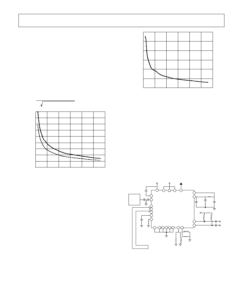
CHOOSING THE CORRECT INDUCTANCE VALUE
The ADF4360-8 can be used at many different frequencies
simply by choosing the external inductors to give the correct
output frequency. Figure 21 shows a graph of both minimum
and maximum frequency versus the external inductor value.
The correct inductor should cover the maximum and minimum
frequencies desired. The inductors used are 0603 CS or 0805 CS
type from Coilcraft. To reduce mutual coupling, the inductors
should be placed at right angles to one another.
The lowest center frequency of oscillation possible is approxi-
mately 65 MHz, which is achieved using 560 nH inductors. This
relationship can be expressed by
(
)
EXT
O
L
F
+
=
nH
0.9
pF
9.3
2
1
0
150
50
100
350
250
300
200
450
400
0
100
200
300
400
600
500
INDUCTANCE (nH)
FRE
Q
UE
NCY
(MHz)
04763-025
Figure 21. Output Center Frequency vs. External Inductor Value
Where F
O
is the center frequency and L
EXT
is the external induc-
tance. The approximate value of capacitance at the midpoint of
the center band of the VCO is 9.3 pF, and the approximate value
of internal inductance due to the bond wires is 0.9 nH. The
VCO sensitivity is a measure of the frequency change versus the
tuning voltage. It is a very important parameter for the low-pass
filter. Figure 22 shows a graph of the tuning sensitivity (in
MHz/V) versus the inductance (nH). It can be seen that as the
inductance increases, the sensitivity decreases. This relationship
can be derived from the equation above, i.e., since the induc-
tance has increased, the change in capacitance from the varactor
has less of an effect on the frequency.
0
4
2
10
8
6
12
0
100
200
300
400
600
500
INDUCTANCE (nH)
SEN
SITIVITY (
M
H
z
/V)
04763-026
Figure 22. Tuning Sensitivity (in MHz/V) vs. Inductance (nH)
FIXED FREQUENCY LO
Figure 23 shows the ADF4360-8 used as a fixed frequency LO at
200 MHz. The low-pass filter was designed using ADIsimPLL
for a channel spacing of 2 MHz and an open-loop bandwidth of
100 kHz. The maximum PFD frequency of the ADF4360-8 is 8
MHz. Since using a larger PFD frequency allows the use of a
smaller N, the in-band phase noise is reduced to as low as
possible, -109 dBc/Hz. The typical rms phase noise (100 Hz to
100 kHz) of the LO in this configuration is 0.09∞. The reference
frequency is from a 16MHz TCXO from Fox; thus, an R value of
2 is programmed. Taking into account the high PFD frequency
and its effect on the band select logic, the band select clock
divider is enabled. In this case, a value of 8 is chosen. A very
simple shunt inductor and dc blocking capacitor complete the RF
output stage.
SPI
-C
OMPA
TI
B
L
E SER
I
A
L B
U
S
ADF4360-8
V
VCO
V
VCO
FOX
801BE-160
16MHz
V
VCO
CPGND
AGND DGND L1 L2 RF
OUT
B
RF
OUT
A
CP
1nF
47pF
68nH
470
68nH
470
22nF
56nH
56nH
680pF
51
100pF
100pF
1nF
1nF
10
µ
F
4.7k
6.8k
15k
R
SET
C
C
LE
DATA
CLK
REF
IN
C
N
V
TUNE
DV
DD
AV
DD
CE MUXOUT
5
4
24
7
20
23
2
21
6
14
16
17
18
19
13
1
3
8
9
10
11 22 15
12
V
VDD
LOCK
DETECT
04763-
027
Figure 23. Fixed Frequency LO
ADF4360-8
Rev. 0 | Page 20 of 24
POWER-UP
After power-up, the part needs three writes for normal opera-
tion. The correct sequence is to the R counter latch, followed by
the control latch, and N counter latch.
INTERFACING
The ADF4360 family has a simple SPIÆ compatible serial inter-
face for writing to the device. CLK, DATA, and LE control the
data transfer. When LE goes high, the 24 bits that have been
clocked into the appropriate register on each rising edge of CLK
are transferred to the appropriate latch. See Figure 2 for the
timing diagram and Table 5 for the latch truth table.
The maximum allowable serial clock rate is 20 MHz. This
means that the maximum update rate possible is 833 kHz or
one update every 1.2 µs. This is certainly more than adequate
for systems that have typical lock times in hundreds of micro-
seconds.
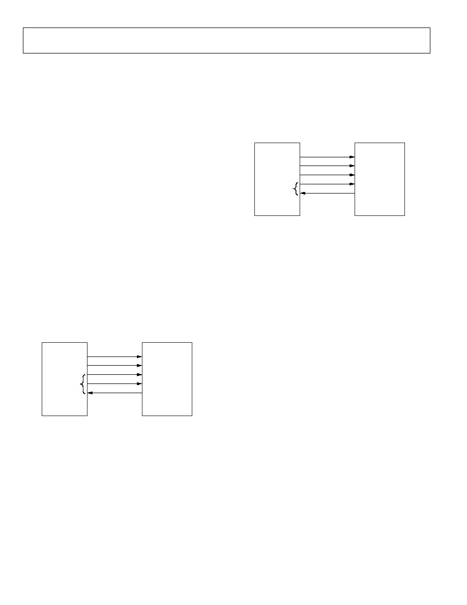
ADuC812 Interface
Figure 24 shows the interface between the ADF4360 family and
the ADuC812 MicroConverterÆ. Since the ADuC812 is based on
an 8051 core, this interface can be used with any 8051-based
microcontrollers. The MicroConverter is set up for SPI master
mode with CPHA = 0. To initiate the operation, the I/O port
driving LE is brought low. Each latch of the ADF4360 family
needs a 24-bit word, which is accomplished by writing three
8-bit bytes from the MicroConverter to the device. After the
third byte has been written, the LE input should be brought
high to complete the transfer.
04763-028
ADuC812
ADF4360-x
SCLK
SDATA
LE
CE
MUXOUT
(LOCK DETECT)
SCLOCK
MOSI
I/O PORTS
Figure 24. ADuC812 to ADF4360-x Interface
I/O port lines on the ADuC812 are also used to control power-
down (CE input) and detect lock (MUXOUT configured as lock
detect and polled by the port input). When operating in the
described mode, the maximum SCLOCK rate of the ADuC812
is 4 MHz. This means that the maximum rate at which the
output frequency can be changed is 166 kHz.
ADSP-2181 Interface
Figure 25 shows the interface between the ADF4360 family and
the ADSP-21xx digital signal processor. The ADF4360 family
needs a 24-bit serial word for each latch write. The easiest way
to accomplish this using the ADSP-21xx family is to use the
autobuffered transmit mode of operation with alternate fram-
ing. This provides a means for transmitting an entire block of
serial data before an interrupt is generated.
04763-029
ADSP-21xx
ADF4360-x
SCLK
SDATA
LE
CE
MUXOUT
(LOCK DETECT)
SCLOCK
MOSI
TFS
I/O PORTS
Figure 25. ADSP-21xx to ADF4360-x Interface
Set up the word length for 8 bits and use three memory loca-
tions for each 24-bit word. To program each 24-bit latch, store
the 8-bit bytes, enable the autobuffered mode, and write to the
transmit register of the DSP. This last operation initiates the
autobuffer transfer.
PCB DESIGN GUIDELINES FOR CHIP SCALE PACKAGE
The leads on the chip scale package (CP-24) are rectangular.
The printed circuit board pad for these should be 0.1 mm
longer than the package lead length and 0.05 mm wider than
the package lead width. The lead should be centered on the pad
to ensure that the solder joint size is maximized.
The bottom of the chip scale package has a central thermal pad.
The thermal pad on the printed circuit board should be at least
as large as this exposed pad. On the printed circuit board, there
should be a clearance of at least 0.25 mm between the thermal
pad and the inner edges of the pad pattern to ensure that short-
ing is avoided.
Thermal vias may be used on the printed circuit board thermal
pad to improve thermal performance of the package. If vias
are used, they should be incorporated into the thermal pad at
1.2 mm pitch grid. The via diameter should be between 0.3 mm
and 0.33 mm, and the via barrel should be plated with 1 ounce
of copper to plug the via.
The user should connect the printed circuit thermal pad to
AGND. This is internally connected to AGND.
ADF4360-8
Rev. 0 | Page 21 of 24
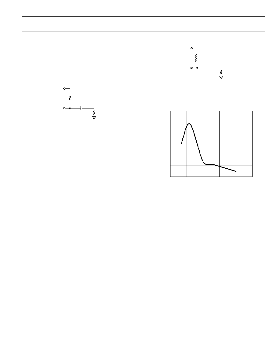
OUTPUT MATCHING
There are a number of ways to match the output of the
ADF4360-8 for optimum operation; the most basic is to use a
50 resistor to V
VCO
. A dc bypass capacitor of 100 pF is
connected in series as shown in Figure 26. Because the resistor
is not frequency dependent, this provides a good broadband
match. The output power in the circuit below typically gives
-9 dBm output power into a 50 load.
L
100pF
04763-031
RF
OUT
V
VCO
50
Figure 27. Optimum ADF4360-8 Output Stage
100pF
04763-030
RF
OUT
V
VCO
50
51
The recommended value of this inductor changes with the VCO
center frequency. A graph of the optimum inductor value versus
frequency is shown in Figure 28.
CENTRE FREQUENCY (MHz)
INDUCTANCE
(nH)
300
250
150
200
100
0
50
0
100
200
300
5000
400
04763-032
Figure 26. Simple ADF4360-8 Output Stage
A better solution is to use a shunt inductor (acting as an RF
choke) to V
VCO.
This gives a better match and, therefore, more
output power.
Experiments have shown that the circuit shown in Figure 27
provides an excellent match to 50 over the operating range of
the ADF4360-8. This gives approximately 0 dBm output power
across the specific frequency range of the ADF4360-8 using the
recommended shunt inductor, followed by a 100 pF dc blocking
capacitor.
Figure 28. Optimum ADF4360-8 Shunt Inductor
Both complementary architectures can be examined using the
EVAL-ADF4360-8EB1 evaluation board. If the user does not
need the differential outputs available on the ADF4360-8, the
user should either terminate the unused output or combine
both outputs using a balun. Alternatively, instead of the LC
balun, both outputs may be combined using a 180∞ rat-race
coupler.
ADF4360-8
Rev. 0 | Page 22 of 24
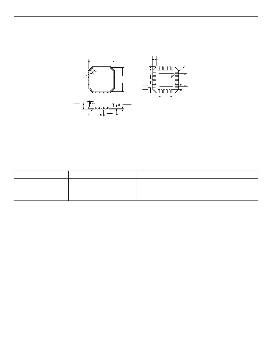
OUTLINE DIMENSIONS
1
24
6
7
13
19
18
12
2.25
2.10 SQ
1.95
0.60 MAX
0.50
0.40
0.30
0.30
0.23
0.18
2.50 REF
0.50
BSC
12∞ MAX
0.80 MAX
0.65 TYP
0.05 MAX
0.02 NOM
1.00
0.85
0.80
SEATING
PLANE
PIN 1
INDICATOR
TOP
VIEW
3.75
BSC SQ
4.00
BSC SQ
PIN 1
INDICATOR
0.60 MAX
COPLANARITY
0.08
0.20 REF
0.25 MIN
EXPOSED
PAD
(BOTTOM VIEW)
COMPLIANT TO JEDEC STANDARDS MO-220-VGGD-2
Figure 29. 24-Lead Lead Frame Chip Scale Package [LFCSP]
4 mm ◊ 4 mm Body (CP-24-1)
Dimensions shown in millimeters
ORDERING GUIDE
Model
Temperature Range
Frequency Range
Package Option
ADF4360-8BCP
-40∞C to +85∞C
65 MHz to 400 MHz
CP-24-1
ADF4360-8BCPRL
-40∞C to +85∞C
65 MHz to 400 MHz
CP-24-1
ADF4360-8BCPRL7
-40∞C to +85∞C
65 MHz to 400 MHz
CP-24-1
EVAL-ADF4360-8EB1
Evaluation
Board

ADF4360-8
Rev. 0 | Page 23 of 24
NOTES

ADF4360-8
Rev. 0 | Page 24 of 24
NOTES
Purchase of licensed I
2
C components of Analog Devices or one of its sublicensed Associated Companies conveys a license for the purchaser under the Philips I
2
C Patent
Rights to use these components in an I
2
C system, provided that the system conforms to the I
2
C Standard Specification as defined by Philips.
© 2004 Analog Devices, Inc. All rights reserved. Trademarks and
registered trademarks are the property of their respective owners.
D04763≠0≠10/04(0)