 | ÐлекÑÑоннÑй компоненÑ: MAT01 | СкаÑаÑÑ:  PDF PDF  ZIP ZIP |
Äîêóìåíòàöèÿ è îïèñàíèÿ www.docs.chipfind.ru
REV. A
Information furnished by Analog Devices is believed to be accurate and
reliable. However, no responsibility is assumed by Analog Devices for its
use, nor for any infringements of patents or other rights of third parties
which may result from its use. No license is granted by implication or
otherwise under any patent or patent rights of Analog Devices.
a
Matched Monolithic
Dual Transistor
MAT01
FEATURES
Low V
OS
(V
BE
Match): 40 V typ, 100 V max
Low TCV
OS
: 0.5 V/ C max
High h
FE
: 500 min
Excellent h
FE
Linearity from 10 nA to 10 mA
Low Noise Voltage: 0.23 V p-p--0.1 Hz to 10 Hz
High Breakdown: 45 V min
Available in Die Form
PRODUCT DESCRIPTION
The MAT01 is a monolithic dual NPN transistor. An exclusive
Silicon Nitride "Triple-Passivation" process provides excellent
stability of critical parameters over both temperature and time.
Matching characteristics include offset voltage of 40
µ
V, tem-
perature drift of 0.15
µ
V/
°
C, and h
FE
matching of 0.7%. Very
high h
FE
is provided over a six decade range of collector current,
including an exceptional h
FE
of 590 at a collector current of only
10 nA. The high gain at low collector current makes the
MAT01 ideal for use in low power, low level input stages.
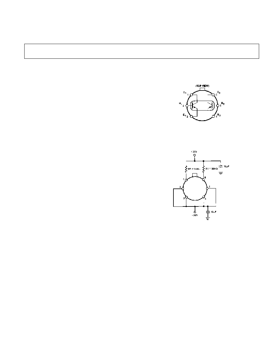
PIN CONNECTION
TO-78
(H Suffix)
NOTE: Substrate is connected to case.
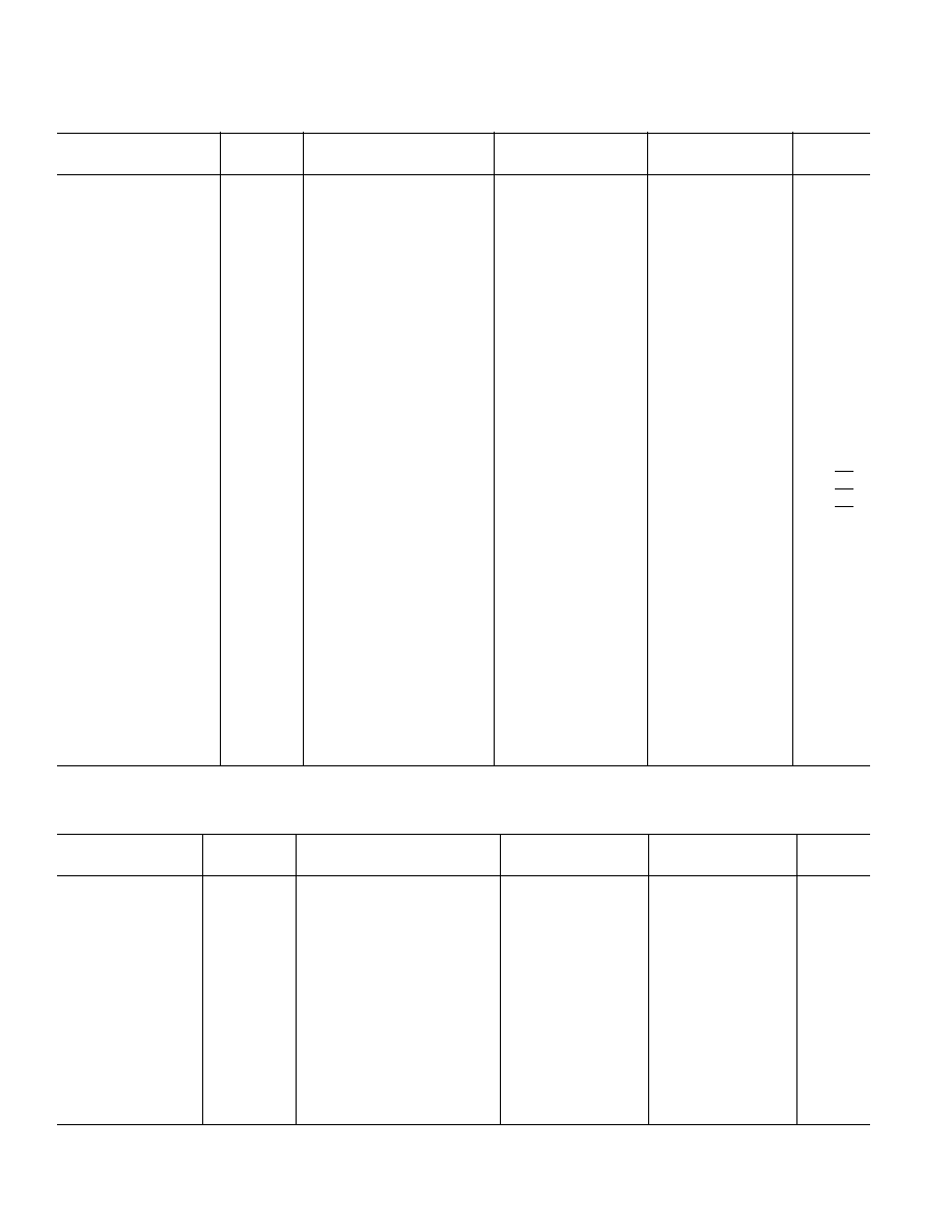
BURN-IN CIRCUIT
One Technology Way, P.O. Box 9106, Norwood, MA 02062-9106, U.S.A.
Tel: 617/329-4700
World Wide Web Site: http://www.analog.com
Fax: 617/326-8703
© Analog Devices, Inc., 1997
REV. A
2
MAT01SPECIFICATIONS
ELECTRICAL CHARACTERISTICS
(@ V
CB
= 15 V, I
C
= 10 A, T
A
= 25 C, unless otherwise noted.)
MAT01AH
MAT01GH
Parameter
Symbol
Conditions
Min
Typ
Max
Min
Typ
Min
Units
Breakdown Voltage
BV
CEO
I
C
= 100
µ
A
45
45
V
Offset Voltage
V
OS
0.04
0.1
0.10
0.5
mV
Offset Voltage Stability
First Month
V
OS
/Time
(Note 1)
2.0
2.0
µ
V/Mo
Long Term
(Note 2)
0.2
0.2
µ
V/Mo
Offset Current
I
OS
0.1
0.6
0.2
3.2
nA
Bias Current
I
B
13
20
18
40
nA
Current Gain
h
FE
I
C
= 10 nA
590
430
I
C
= 10
µ
A
500
770
250
560
I
C
= 10 mA
840
610
Current Gain Match
h
FE
I
C
= 10
µ
A
0.7
3.0
1.0
8.0
%
100 nA
I
C
10 mA
0.8
1.2
%
Low Frequency Noise
Voltage
e
n
p-p
0.1 Hz to 10 Hz
3
0.23
0.4
0.23
0.4
µ
V p-p
Broadband Noise
Voltage
e
n
rms
1 Hz to 10 kHz
0.60
0.60
µ
V rms
Noise Voltage
Density
e
n
f
O
= 10 Hz
3
7.0
9.0
7.0
9.0
nV/
Hz
f
O
= 100 Hz
3
6.1
7.6
6.1
7.6
nV/
Hz
f
O
= 1000 Hz
3
6.0
7.5
6.0
7.5
nV/
Hz
Offset Voltage Change
V
OS/
V
CB
0
V
CB
30 V
0.5
3.0
0.8
8.0
µ
V/V
Offset Current Change
I
OS/
V
CB
0
V
CB
30 V
2
15
3
70
pA/V
Collector-Base
Leakage Current
I
CBO
V
CB
= 30 V, I
E
= 0
4
15
50
25
200
pA
Collector-Emitter
Leakage Current
I
CES
V
CE
= 30 V, V
BE
= 0
4, 5
50
200
90
400
pA
Collector-Collector
Leakage Current
I
CC
V
CC
= 30 V
5
20
200
30
400
pA
Collector Saturation
V
CE(SAT)
I
B
= 0.1 mA, I
C
= 1 mA
0.12
0.20
0.12
0.25
V
Voltage
I
B
= 1 mA, I
C
= 10 mA
0.8
0.8
V
Gain-Bandwidth Product
f
T
V
CE
= 10 V, I
C
= 10 mA
450
450
MHz
Output Capacitance
C
OB
V
CB
= 15 V, I
E
= 0
2.8
2.8
pF
Collector-Collector
Capacitance
C
CC
V
CC
= 0
8.5
8.5
pF
ELECTRICAL CHARACTERISTICS
MAT01AH
MAT01GH
Parameter
Symbol
Conditions
Min
Typ
Max
Min
Typ
Min
Units
Offset Voltage
V
OS
0.06
0.15
0.14
0.70
mV
Average Offset
Voltage Drift
TCV
OS
(Note 6)
0.15
0.50
0.35
1.8
µ
V/
°
C
Offset Current
I
OS
0.9
8.0
1.5
15.0
nA
Average Offset
Current Drift
TCI
OS
(Note 7)
10
90
15
150
pA/
°
C
Bias Current
28
60
36
130
nA
Current Gain
h
FE
167
400
77
300
Collector-Base
I
CBO
T
A
= 125
°
C, V
CB
= 30 V,
Leakage Current
I
E
= 0
4
15
80
25
200
nA
Collector-Emitter
I
CES
T
A
= 125
°
C, V
CE
= 30 V,
Leakage Current
V
BE
= 0
4, 6
50
300
90
400
nA
Collector-Collector
I
CC
T
A
= 125
°
C, V
CC
= 30 V,
Leakage Current
(Note 6)
30
200
50
400
nA
(@ V
CB
= 15 V, I
C
= 10 A, 55 C
T
A
+125 C, unless otherwise noted.)

TYPICAL ELECTRICAL CHARACTERISTICS
MAT01N
Parameter
Symbol
Conditions
Typical
Units
Average Offset Voltage Drift
TCV
OS
0.35
µ
V/
°
C
Average Offset Current Drift
TCI
OS
15
pA/
°
C
Collector-Emitter-Leakage
Current
I
CES
V
CE
= 30 V, V
BE
= 0
90
pA
Collector-Base-Leakage
Current
I
CBO
V
CB
= 30 V, I
E
= 0
25
pA
Gain Bandwidth Product
f
T
V
CE
= 10 V, I
C
= 10 mA
450
MHz
Offset Voltage Stability
V
OS
/T
First Month (Note 1)
2.0
µ
V/Mo
Long-Term (Note 2)
0.2
µ
V/Mo
(@ V
CB
= 15 V and I
C
= 10 A, T
A
= +25 C, unless otherwise noted.)
NOTES
1
Exclude first hour of operation to allow for stabilization.
2
Parameter describes long-term average drift after first month of operation.
3
Sample tested.
4
The collector-base (I
CBO
) and collector-emitter (I
CES
) leakage currents may be
reduced by a factor of two to ten times by connecting the substrate (package) to
a potential which is lower than either collector voltage.
5
I
CC
and I
CES
are guaranteed by measurement of I
CBO
.
6
Guaranteed by V
OS
test (TCV
OS
V
OS
T
for V
OS
V
BE
) T = 298
°
K for T
A
= 25
°
C.
7
Guaranteed by I
OS
test limits over temperature.
Specifications subject to change without notice.
MAT01
3
REV. A
WAFER TEST LIMITS
MAT01N
Parameter
Symbol
Conditions
Limits
Units
Breakdown Voltage
BV
CEO
I
C
= 100
µ
A
45
V min
Offset Voltage
V
OS
0.5
mV max
Offset Current
I
OS
3.2
nA max
Bias Current
I
B
40
nA max
Current Gain
h
FE
250
min
Current Gain Match
h
FE
8.0
% max
Offset Voltage Change
V
OS
/
V
CB
0
V
CB
30 V
8.0
µ
V/V max
Offset Current Change
V
OS
/
V
CB
0
V
CB
30 V
70
pA/V max
Collector Saturation Voltage
V
CE (SAT)
I
B
= 0.1 mA, I
C
= 1 mA
0.25
V max
NOTE
Electrical tests are performed at wafer probe to the limits shown. Due to variations in assembly methods and normal yield loss, yield after packaging is not
guaranteed for standard product dice. Consult factory to negotiate specifications based on dice lot qualification through sample lot assembly and testing.
(@ V
CB
= 15 V, I
C
= 10 A, T
A
= +25 C, unless otherwise noted.)
MAT01
4
REV. A
ABSOLUTE MAXIMUM RATINGS
1
Collector-Base Voltage (BV
CBO
)
MAT01AH, GH, N . . . . . . . . . . . . . . . . . . . . . . . . . . . 45 V
Collector-Emitter Voltage (BV
CEO
)
MAT01AH, GH, N . . . . . . . . . . . . . . . . . . . . . . . . . . . 45 V
Collector-Collector Voltage (BV
CC
)
MAT01AH, GH, N . . . . . . . . . . . . . . . . . . . . . . . . . . . 45 V
Emitter-Emitter Voltage (BV
EE
)
MAT01AH, GH, N . . . . . . . . . . . . . . . . . . . . . . . . . . . 45 V
Emitter-Base Voltage (BV
EBO
)
2
. . . . . . . . . . . . . . . . . . . . . 5 V
Collector Current (I
C
) . . . . . . . . . . . . . . . . . . . . . . . . . .25 mA
Emitter Current (I
E
) . . . . . . . . . . . . . . . . . . . . . . . . . . 25 mA
Total Power Dissipation
Case Temperature
40
°
C
3
. . . . . . . . . . . . . . . . . . . . 1.8 W
Ambient Temperature
70
°
C
4
. . . . . . . . . . . . . . . 500 mW
Operating Ambient Temperature . . . . . . . . . 55
°
C to +125
°
C
Operating Junction Temperature . . . . . . . . . 55
°
C to +150
°
C
Storage Temperature . . . . . . . . . . . . . . . . . . 65
°
C to +150
°
C
Lead Temperature (Soldering, 60 sec) . . . . . . . . . . . . +300
°
C
DICE Junction Temperature . . . . . . . . . . . . 65
°
C to +150
°
C
NOTES
1
Absolute maximum ratings apply to both DICE and packaged devices.
2
Application of reverse bias voltages in excess of rating shown can result in
degradation of h
FE
and h
FE
matching characteristics. Do not attempt to measure
BV
EBO
greater than the 5 V rating shown.
3
Rating applies to applications using heat sinking to control case temperature.
Derate linearity at 16.4 mW/
°
C for case temperatures above 40
°
C.
4
Rating applies to applications not using heat sinking; device in free air only. Derate
linearity at 6.3 mW/
°
C for ambient temperatures above 70
°
C.
ORDERING GUIDE
1
V
OS
max
Temperature
Package
Model
(T
A
= +25 C)
Range
Option
MAT01AH
2
0.1 mV
55
°
C to +125
°
C
TO-78
MAT01GH
0.5 mV
55
°
C to +125
°
C
TO-78
NOTES
1
Burn-in is available on commercial and industrial temperature range parts in
TO-can packages.
2
For devices processed in total compliance to MIL-STD-883, add/883 after part
number. Consult factory for 883 data sheet.
WARNING!
ESD SENSITIVE DEVICE
CAUTION
ESD (electrostatic discharge) sensitive device. Electrostatic charges as high as 4000 V readily
accumulate on the human body and test equipment and can discharge without detection.
Although the MAT01 features proprietary ESD protection circuitry, permanent damage may
occur on devices subjected to high energy electrostatic discharges. Therefore, proper ESD
precautions are recommended to avoid performance degradation or loss of functionality.
DICE CHARACTERISTICS
DIE SIZE 0.035
×
0.025 inch, 875 sq. mils
(0.89
×
0.64 mm, 0.58 sq. mm)
1. COLLECTOR (1)
2. BASE (1)
3. EMITTER (1)
5. EMITTER (2)
6. BASE (2)
7. COLLECTOR (2)
MAT01
5
REV. A
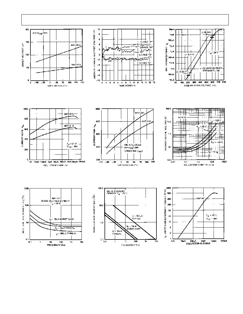
Figure 1. Offset Voltage
vs. Temperature
Figure 2. Current Gain
vs. Collector Current
Figure 3. Noise Voltage
Figure 7. Base-Emitter Voltage
vs. Collector Current
Figure 8. Saturation Voltage
vs. Collector Current
Figure 9. Gain-Bandwidth
vs. Collector Current
Figure 4. Offset Voltage vs. Time
Figure 5. Current Gain
vs. Temperature
Figure 6. Noise Current Density
MAT01
6
REV. A
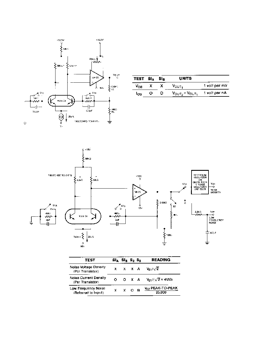
MAT01 TEST CIRCUITS
Figure 10. MAT01 Matching Measurement Circuit
Figure 11. MAT01 Noise Measurement Circuit
MAT01
7
REV. A
APPLICATION NOTES
Application of reverse bias voltages to the emitter-base junctions
in excess of ratings (5 V) may result in degradation of h
FE
and
h
FE
matching characteristics. Circuit designs should be checked
to ensure that reverse bias voltages above 5 V cannot be applied
during such transient conditions as at circuit turn-on and
turn-off.
Stray thermoelectric voltages generated by dissimilar metals at
the contacts to the input terminals can prevent realization of the
predicted drift performance. Both input terminals should be
maintained at the same temperature, preferably close to the tem-
perature of the device's package.
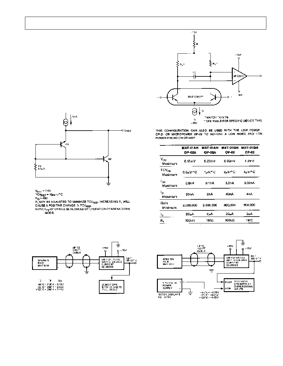
TYPICAL APPLICATIONS
Figure 12. Precision Reference
Figure 13. Basic Digital Thermometer Readout in
Degrees Kelvin (
°
K)
Figure 14. Precision Operational Amplifiers
Figure 15. Digital Thermometer with Readout in
°
C
MAT01
8
REV. A
312706/97
PRINTED IN U.S.A.
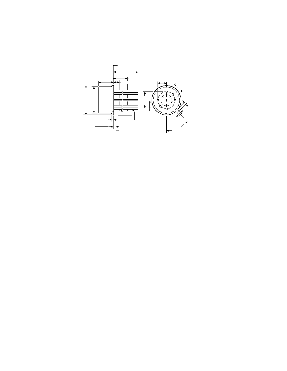
OUTLINE DIMENSIONS
Dimensions shown in inches and (mm).
H-06A
6-Lead Metal Can (TO-78)
0.250 (6.35) MIN
0.750 (19.05)
0.500 (12.70)
0.185 (4.70)
0.165 (4.19)
REFERENCE PLANE
0.050 (1.27) MAX
0.019 (0.48)
0.016 (0.41)
0.021 (0.53)
0.016 (0.41)
0.045 (1.14)
0.010 (0.25)
0.040 (1.02) MAX
BASE & SEATING PLANE
0.335 (8.51)
0.305 (7.75)
0.370 (9.40)
0.335 (8.51)
0.034 (0.86)
0.027 (0.69)
0.045 (1.14)
0.027 (0.69)
0.160 (4.06)
0.110 (2.79)
0.100 (2.54) BSC
5
2
6
4
3
1
0.200
(5.08)
BSC
0.100
(2.54)
BSC
45
°
BSC