 | –≠–ª–µ–∫—Ç—Ä–æ–Ω–Ω—ã–π –∫–æ–º–ø–æ–Ω–µ–Ω—Ç: MAT02E | –°–∫–∞—á–∞—Ç—å:  PDF PDF  ZIP ZIP |
MAT02 DS
a
Low Noise, Matched
Dual Monolithic Transistor
MAT02
FEATURES
Low Offset Voltage: 50 V max
Low Noise Voltage at 100 Hz, 1 mA: 1.0 nV/
Hz max
High Gain (h
FE
):
500 min at I
C
= 1 mA
300 min at I
C
= 1 A
Excellent Log Conformance: r
BE
0.3
Low Offset Voltage Drift: 0.1 V/ C max
Improved Direct Replacement for LM194/394
NOTE
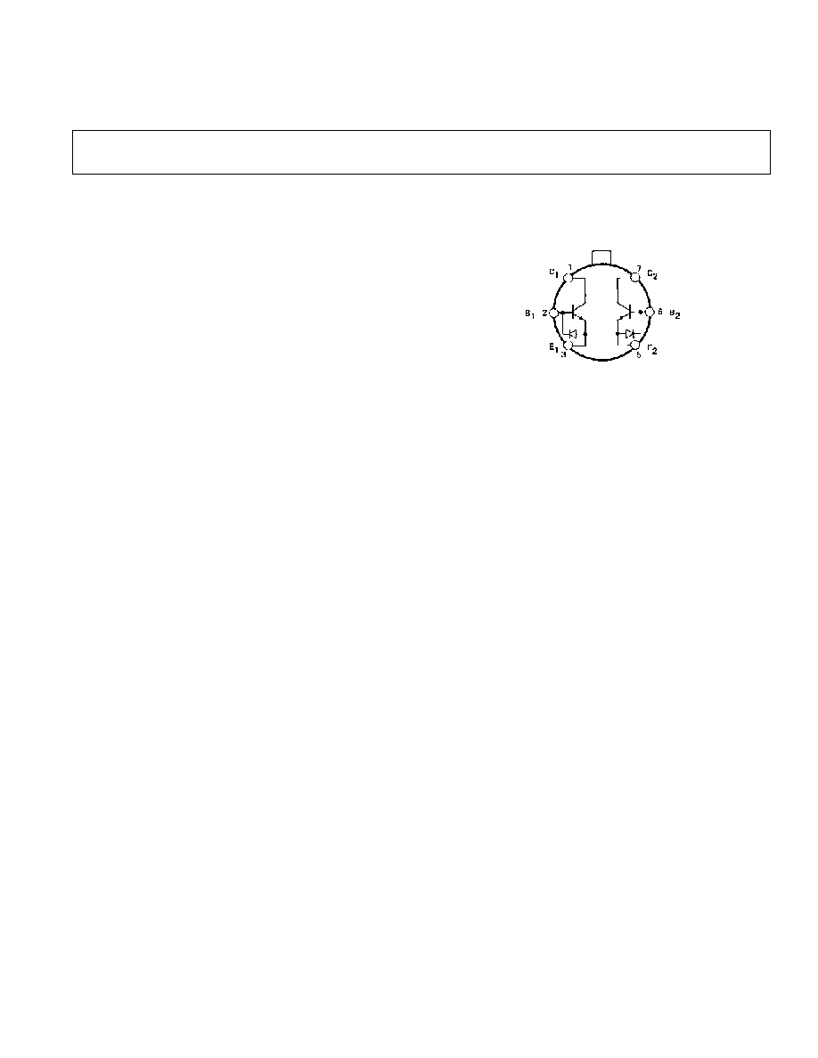
Substrate is connected to case on TO-78 package.
Substrate is normally connected to the most negative
circuit potential, but can be floated.
PIN CONNECTION
TO-78
(H Suffix)
PRODUCT DESCRIPTION
The design of the MAT02 series of NPN dual monolithic tran-
sistors is optimized for very low noise, low drift and low r
BE
.
Precision Monolithics' exclusive Silicon Nitride "Triple-
Passivation" process stabilizes the critical device parameters
over wide ranges of temperature and elapsed time. Also, the high
current gain (h
FE
) of the MAT02 is maintained over a wide
range of collector current. Exceptional characteristics of the
MAT02 include offset voltage of 50
µV max (A/E grades) and
150
µV max F grade. Device performance is specified over the
full military temperature range as well as at 25
∞C.
Input protection diodes are provided across the emitter-base
junctions to prevent degradation of the device characteristics
due to reverse-biased emitter current. The substrate is clamped
to the most negative emitter by the parasitic isolation junction
created by the protection diodes. This results in complete isola-
tion between the transistors.
Information furnished by Analog Devices is believed to be accurate and
reliable. However, no responsibility is assumed by Analog Devices for its
use, nor for any infringements of patents or other rights of third parties that
may result from its use. No license is granted by implication or otherwise
under any patent or patent rights of Analog Devices.
One Technology Way, P.O. Box 9106, Norwood, MA 02062-9106, U.S.A.
Tel: 781/329-4700
www.analog.com
Fax: 781/326-8703
© Analog Devices, Inc., 2002
REV. E
The MAT02 should be used in any application where low
noise is a priority. The MAT02 can be used as an input
stage to make an amplifier with noise voltage of less than
1.0 nV/
Hz at 100 Hz. Other applications, such as log/antilog
circuits, may use the excellent logging conformity of the
MAT02. Typical bulk resistance is only 0.3
to 0.4 . The
MAT02 electrical characteristics approach those of an ideal
transistor when operated over a collector current range of 1
µA to 10 mA. For applications requiring multiple devices
see MAT04 Quad Matched Transistor data sheet.
REV. E
≠2≠
ELECTRICAL CHARACTERISTICS
MAT02E MAT02F
Parameter
Symbol
Conditions
Min
Typ
Max
Min
Typ
Max
Unit
Current Gain
h
FE
I
C
= 1 mA
1
500
605
400
605
I
C
= 100
µA
500
590
400
590
I
C
= 10
µA
400
550
300
550
I
C
= 1
µA
300
485
200
485
Current Gain Match
h
FE
10
µA I
C
1 mA
2
0.5
2
0.5
4
%
Offset Voltage
V
OS
V
CB
= 0, 1
µA I
C
1 mA
3
10
50
80
150
µV
Offset Voltage
V
OS
/
V
CB
0
V
CB
V
MAX
4
10
25
10
50
µV
Change vs. V
CB
1
µA I
C
1 mA
3
10
25
10
50
µV
Offset Voltage Change
V
OS
/
I
C
V
CB
= 0 V
5
25
5
50
µV
vs. Collector Current
1
µA I
C
1 mA
3
5
25
5
50
µV
Offset Current
Change vs. V
CB
I
OS
/
V
CB
0
V
CB
V
MAX
30
70
30
70
pA/V
Bulk Resistance
r
BE
10
µA I
C
10 mA
5
0.3
0.5
0.3
0.5
Collector-Base
Leakage Current
I
CBO
V
CB
= V
MAX
25
200
25
400
pA
Collector-Collector
Leakage Current
I
CC
V
CC
= V
MAX
5, 6
35
200
35
400
pA
Collector-Emitter
V
CE
= V
MAX
5, 6
Leakage Current
I
CES
V
BE
= 0
35
200
35
400
pA
Noise Voltage Density
e
n
I
C
= 1 mA, V
CB
= 0
7
f
O
= 10 Hz
1.6
2
1.6
3
nV/
Hz
f
O
= 100 Hz
0.9
1
0.9
2
nV/
Hz
f
O
= 1 kHz
0.85
1
0.85
2
nV/
Hz
f
O
= 10 kHz
0.85
1
0.85
2
nV/
Hz
Collector Saturation
Voltage
V
CE(SAT)
I
C
= 1 mA, I
B
= 100
µA
0.05
0.1
0.05
0.2
V
Input Bias Current
I
B
I
C
= 10
µA
25
34
nA
Input Offset Current
I
OS
I
C
= 10
µA
0.6
1.3
nA
Breakdown Voltage
BV
CEO
40
40
V
Gain-Bandwidth Product
f
T
I
C
= 10 mA, V
CE
= 10 V
200
200
MHz
Output Capacitance
C
OB
V
CB
= 15 V, I
E
= 0
23
23
pF
Collector-Collector
Capacitance
C
CC
V
CC
= 0
35
35
pF
NOTES
1
Current gain is guaranteed with Collector-Base Voltage (V
CB
) swept from 0 to V
MAX
at the indicated collector currents.
2
Current gain match (
h
FE
) is defined as:
h
FE =
3
Measured at I
C
= 10
µA and guaranteed by design over the specified range of I
C
.
4
This is the maximum change in V
OS
as V
CB
is swept from 0 V to 40 V.
5
Guaranteed by design.
6
I
CC
and I
CES
are verified by measurement of I
CBO
.
7
Sample tested.
Specifications subject to change without notice.
100 (
I
B
) (h
FE
min)
I
C
MAT02≠SPECIFICATIONS
(@ V
CB
= 15 V, I
C
= 10 A, T
A
= 25 C, unless otherwise noted.)
ELECTRICAL CHARACTERISTICS
MAT02E MAT02F
Parameter
Symbol
Conditions
Min
Typ
Max
Min
Typ
Max
Unit
Offset Voltage
V
OS
V
CB
= 0
70
220
µV
1
µA I
C
1 mA
1
Average Offset
Voltage Drift
TCV
OS
10
µA I
C
1 mA, 0 V
CB
V
MAX
2
0.08 0.3
0.08 1
µV/∞C
V
OS
Trimmed to Zero
3
0.03 0.1
0.03 0.3
Input Offset Current
I
OS
I
C
= 10
µA
8
13
nA
Input Offset
Current Drift
TCI
OS
I
C
= 10
µA
4
40
90
40
150
pA/
∞C
Input Bias Current
I
B
I
C
= 10
µA
45
50
nA
Current Gain
h
FE
I
C
= 1 mA
5
325
300
I
C
= 100
µA
275
250
I
C
= 10
µA
225
200
I
C
= 1
µA
200
150
Collector-Base
I
CBO
V
CB
= V
MAX
2
3
nA
Leakage Current
Collector-Emitter
I
CES
V
CE
= V
MAX
, V
BE
= 0
3
4
nA
Leakage Current
Collector-Collector
I
CC
V
CC
= V
MAX
3
4
nA
Leakage Current
NOTES
1
Measured at I
C
= 10
µA and guaranteed by design over the specified range of I
C
.
2
Guaranteed by V
OS
test (TCV
OS
V
T
OS
for V
OS
V
BE
) T = 298K for T
A
= 25
∞C.
3
The initial zero offset voltage is established by adjusting the ratio of I
C
1 to I
C
2 at T
A
= 25
∞C. This ratio must be held to 0.003% over the entire temperature range.
Measurements are taken at the temperature extremes and 25
∞C.
4
Guaranteed by design.
5
Current gain is guaranteed with Collector-Base Voltage (V
CB
) swept from 0 V to V
MAX
at the indicated collector current.
Specifications subject to change without notice.
(V
CB
= 15 V, ≠25 C
T
A
+85 C, unless otherwise noted.)
MAT02
≠3≠
REV. E
WARNING!
ESD SENSITIVE DEVICE
CAUTION
ESD (electrostatic discharge) sensitive device. Electrostatic charges as high as 4000 V readily
accumulate on the human body and test equipment and can discharge without detection.
Although the MAT02 features proprietary ESD protection circuitry, permanent damage may
occur on devices subjected to high energy electrostatic discharges. Therefore, proper ESD
precautions are recommended to avoid performance degradation or loss of functionality.
ABSOLUTE MAXIMUM RATINGS
1
Collector-Base Voltage (BV
CBO
) . . . . . . . . . . . . . . . . . . . . 40 V
Collector-Emitter Voltage (BV
CEO
) . . . . . . . . . . . . . . . . . . 40 V
Collector-Collector Voltage (BV
CC
) . . . . . . . . . . . . . . . . . . 40 V
Emitter-Emitter Voltage (BV
EE
) . . . . . . . . . . . . . . . . . . . . 40 V
Collector Current (I
C
) . . . . . . . . . . . . . . . . . . . . . . . . . . 20 mA
Emitter Current (I
E
) . . . . . . . . . . . . . . . . . . . . . . . . . . . 20 mA
Total Power Dissipation
Case Temperature
40∞C
2
. . . . . . . . . . . . . . . . . . . . . 1.8 W
Ambient Temperature
70∞C
3
. . . . . . . . . . . . . . . . 500 mW
Operating Temperature Range
MAT02E, F . . . . . . . . . . . . . . . . . . . . . . . . . ≠25
∞C to +85∞C
ORDERING GUIDE
V
OS
max
Temperature
Package
Model
(T
A
= 25 C)
Range
Option
MAT02EH
50
µV
≠25
∞C to +85∞C
TO-78
MAT02FH
150
µV
≠25
∞C to +85∞C
TO-78
Operating Junction Temperature . . . . . . . . . . ≠55
∞C to +150∞C
Storage Temperature . . . . . . . . . . . . . . . . . . . ≠65
∞C to +150∞C
Lead Temperature (Soldering, 60 sec) . . . . . . . . . . . . . 300
∞C
Junction Temperature . . . . . . . . . . . . . . . . . . ≠65
∞C to +150∞C
NOTES
1
Absolute maximum ratings apply to both DICE and packaged devices.
2
Rating applies to applications using heat sinking to control case temperature.
Derate linearly at 16.4 mW/
∞C for case temperature above 40∞C.
3
Rating applies to applications not using a heat sinking; devices in free air only.
Derate linearly at 6.3 mW/
∞C for ambient temperature above 70∞C.
MAT02
≠4≠
REV. E
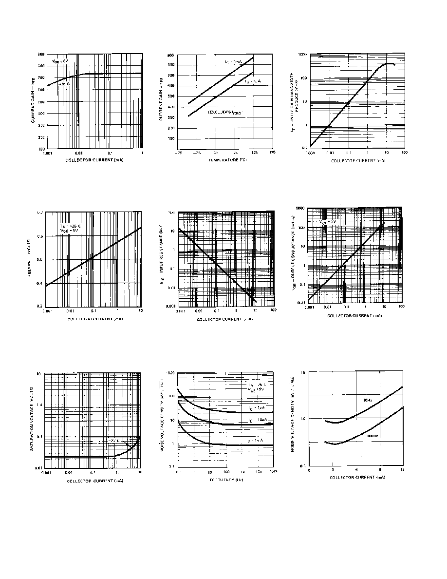
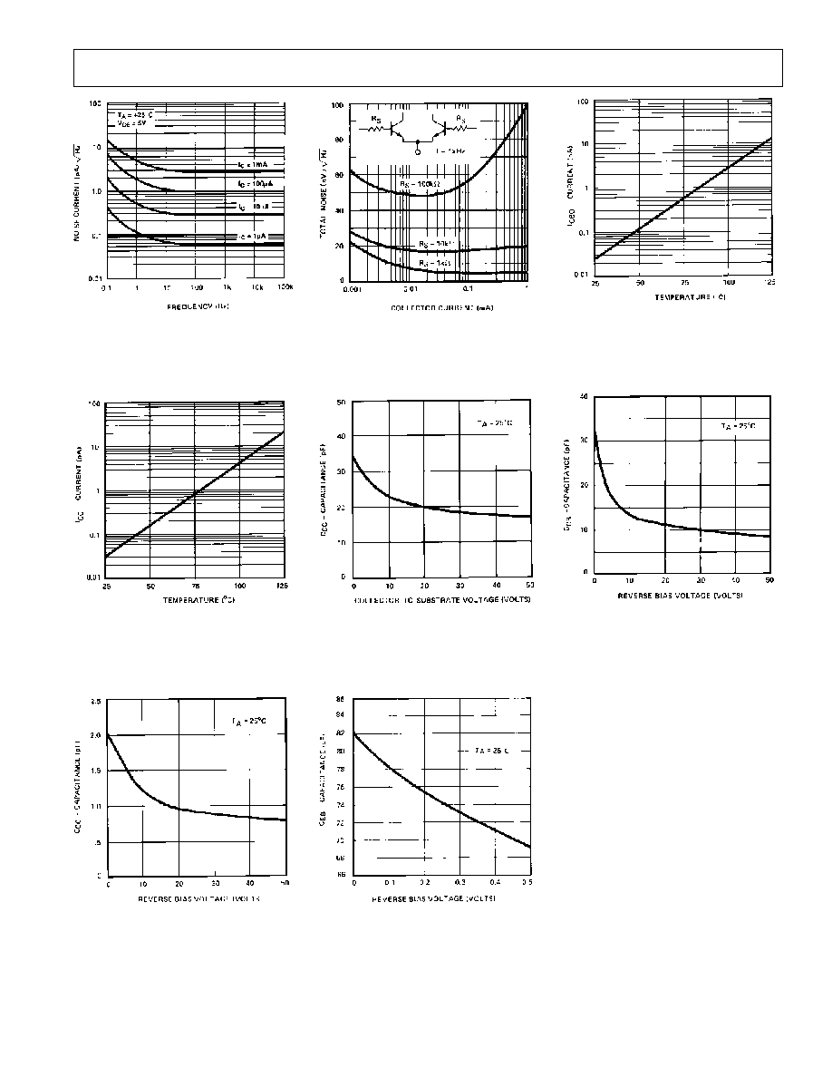
TPC 1. Current Gain vs.
Collector Current
TPC 4. Base-Emitter-On
Voltage vs. Collector Current
TPC 7. Saturation Voltage
vs. Collector Current
TPC 2. Current Gain
vs. Temperature
TPC 5. Small Signal Input
Resistance vs. Collector Current
TPC 8. Noise Voltage
Density vs. Frequency
TPC 3. Gain Bandwidth
vs. Collector Current
TPC 6. Small-Signal Output
Conductance vs. Collector Current
TPC 9. Noise Voltage Density
vs. Collector Current
≠Typical Performance Characteristics
MAT02
≠5≠
REV. E
TPC 10. Noise Current
Density vs. Frequency
TPC 13. Collector-to-Collector
Leakage vs. Temperature
TPC 12. Collector-to-Base
Leakage vs. Temperature
TPC 15. Collector-Base
Capacitance vs. Reverse Bias Voltage
TPC 17. Emitter-Base Capacitance
vs. Reverse Bias Voltage
TPC 16. Collector-to-Collector
Capacitance vs. Reverse Bias
Voltage
TPC 11. Total Noise vs.
Collective Current
TPC 14. Collector-to-Collector
Capacitance vs. Collector-to
Substrate Voltage
MAT02
≠6≠
REV. E
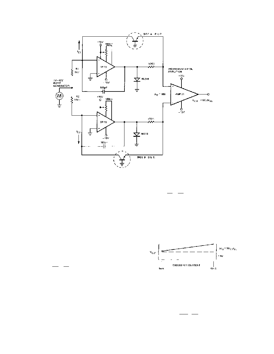
Figure 1. Log Conformance Test Circuit
LOG CONFORMANCE TESTING
The log conformance of the MAT02 is tested using the circuit
shown above. The circuit employs a dual transdiode logarithmic
converter operating at a fixed ratio of collector currents that are
swept over a 10:1 range. The output of each transdiode converter
is the V
BE
of the transistor plus an error term which is the prod-
uct of the collector current and r
BE
, the bulk emitter resistance.
The difference of the V
BE
is amplified at a gain of
◊100 by the
AMP01 instrumentation amplifier. The differential emitter-base
voltage (
V
BE
) consists of a temperature-dependent dc level plus
an ac error voltage, which is the deviation from true log confor-
mity as the collector currents vary.
The output of the transdiode logarithmic converter comes from
the idealized intrinsic transistor equation (for silicon):
V
kT
q
In
I
I
BE
C
S
=
(1)
where
k = Boltzmann's Constant (1.38062
◊ 10
≠23
J/K)
q = Unit Electron Charge (1.60219
◊ 10
≠19
∞C)
T = Absolute Temperature, K (=
∞C + 273.2)
I
S
= Extrapolated Current for V
BE
0
I
C
= Collector Current
An error term must be added to this equation to allow for the
bulk resistance (r
BE
) of the transistor. Error due to the op amp
input current is limited by use of the OP15 BiFET-input op
amp. The resulting AMP01 input is:
V
BE
=
kT
q
In
I
C1
I
C2
+ I
C1
r
BE1
≠ I
C2
r
BE2
(2)
A ramp function that sweeps from 1 V to 10 V is converted by
the op amps to a collector current ramp through each transistor.
Because I
C1
is made equal to 10 I
C2
, and assuming T
A
= 25
∞C,
the previous equation becomes:
V
BE
= 59 mV + 0.9 I
C1
r
BE
(
r
BE
~ 0)
As viewed on an oscilloscope, the change in
V
BE
for a 10:1
change in I
C
is then displayed as shown in Figure 2 below:
Figure 2.
With the oscilloscope ac coupled, the temperature dependent
term becomes a dc offset and the trace represents the deviation
from true log conformity. The bulk resistance can be calculated
from the voltage deviation
V
O
and the change in collector
current (9 mA):
r
BE
=
V
O
9 mA
◊
1
100
(3)
This procedure finds r
BE
for Side A. Switching R
1
and R
2
will
provide the r
BE
for Side B. Differential r
BE
is found by making
R
1
= R
2
.
MAT02
≠7≠
REV. E
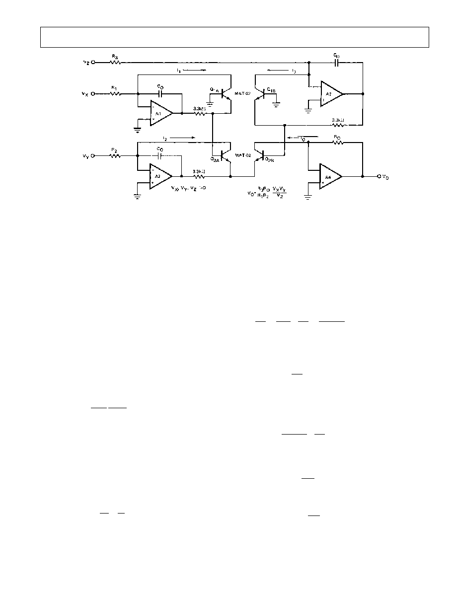
Figure 3. One-Quadrant Multiplier/Divider
APPLICATIONS: NONLINEAR FUNCTIONS
MULTIPLIER/DIVIDER CIRCUIT
The excellent log conformity of the MAT02 over a very wide
range of collector current makes it ideal for use in log-antilog
circuits. Such nonlinear functions as multiplying, dividing,
squaring and square-rooting are accurately and easily imple-
mented with a log antilog circuit using two MAT02 pairs (see
Figure 3). The transistor circuit accepts three input currents (I
1
,
I
2
and I
3
) and provides an output current I
O
according to
I
O
= I
1
I
2
/I
3
. All four currents must be positive in the log antilog
circuit, but negative input voltages can be easily accommodated
by various offsetting techniques. Protective diodes across each
base-to-emitter junction would normally be needed, but these
diodes are built into the MAT02. External protection diodes
are, therefore, not needed.
For the circuit shown in Figure 3, the operational amplifiers
make I
1
= V
X
/R
1
, I
2
= V
Y
/R
2
, I
3
= V
Z
/R
3
, and I
O
= V
O
/R
O
. The
output voltage for this one-quadrant, log-antilog multiplier/
divider is ideally:
V
O
=
R
3
R
O
R
1
R
2
V
X
V
Y
V
Z
(V
X
, V
Y
, V
Z
> 0)
(4)
If all the resistors (R
O
, R
1
, R
2
, R
3
) are made equal, then
V
O
= V
X
V
Y
/V
Z
Resistor values of 50 k
to 100 k are recommended assuming
an input range of 0.1 V to +10 V.
ERROR ANALYSIS
The base-to-emitter voltage of the MAT02 in its forward active
operation is:
V
BE
=
kT
q
In
I
C
I
S
+ r
BE
I
C
, V
CB
~ 0
(5)
The first term comes from the idealized intrinsic transistor
equation previously discussed (see equation (1)).
Extrinsic resistive terms and the early effect cause departure
from the ideal logarithmic relationship. For small V
CB
, all of
these effects can be lumped together as a total effective bulk
resistance r
BE
. The r
BE
I
C
term causes departure from the desired
logarithmic relationship. The r
BE
term for the MAT02 is less
than 0.5
and r
BE
between the two sides is negligible.
Returning to the multiplier/divider circuit of Figure 1 and using
Equation (4):
V
BE1A
+ V
BE2A
≠ V
BE2B
≠ V
BE1B
+ (I
1
+ I
2
≠ I
O
≠ I
3
) r
BE
= 0
If the transistor pairs are held to the same temperature, then:
kT
q
In
I I
I I
kT
q
In
I
I
I
I
O
S A S A
S B S B
1 2
3
1
2
1
2
=
+ (I
1
+ I
2
≠ I
O
≠ I
3
) r
BE
(6)
If all the terms on the right-hand side were zero, then In
(I
1
I
2
/I
3
I
O
) would equal zero, which would lead directly to
the desired result:
I
O
=
I
1
I
2
I
3
, where I
1
, I
2
, I
3
, I
O
> 0
(7)
Note that this relationship is temperature independent. The
right-hand side of Equation (6) is near zero and the output
current I
O
will be approximately I
1
I
2
/I
3
. To estimate error,
define ¯ as the right-hand side terms of Equation (6):
¯ = In
I
I
I
I
q
kT
S A S A
S B S B
1
2
1
2
+
(I
1
+ I
2
≠ I
O
≠ I
3
) r
BE
(8)
For the MAT02, In (I
SA
/I
SB
) and I
C
r
BE
are very small. For small
¯,
ÿ
~ 1 + ¯ and therefore:
I
1
I
2
I
3
I
O
= 1 + ¯
(9)
I
O
~
I
1
I
2
I
3
(1 ≠ ¯)
The In (I
SA
/I
SB
) terms in ¯ cause a fixed gain error of less than
±0.6% from each pair when using the MAT02, and this gain
error is easily trimmed out by varying R
O
. The I
OUT
terms are
MAT02
≠8≠
REV. E
more troublesome because they vary with signal levels and are
multiplied by absolute temperature. At 25
∞C, kT/q is
approximately 26 mV and the error due to an r
BE
I
C
term will be
r
BE
I
C
/26 mV. Using an r
BE
of 0.4
for the MAT02 and assum-
ing a collector current range of up to 200
µA, then a peak error
of 0.3% could be expected for an r
BE
I
C
error term when using
the MAT02. Total error is dependent on the specific application
configuration (multiply, divide, square, etc.) and the required
dynamic range. An obvious way to reduce I
C
r
BE
error is to re-
duce the maximum collector current, but then op amp offsets
and leakage currents become a limiting factor at low input lev-
els. A design range of no greater than 10
µA to 1 mA is generally
recommended for most nonlinear function circuits.
A powerful technique for reducing error due to I
C
r
BE
is shown in
Figure 4. A small voltage equal to I
C
r
BE
is applied to the transis-
tor base. For this circuit:
V
B
=
R
C
R
2
V
1
and I
C
r
BE
=
r
BE
R
1
V
1
(10)
The error from r
BE
I
C
is cancelled if R
C
/R
2
is made equal to r
OUT
R
1
.
Since the MAT02 bulk resistance is approximately 0.39
, an
R
C
of 3.9
and R
2
of 10 R
1
will give good error cancellation.
In more complex circuits, such as the circuit in Figure 3, it may
be inconvenient to apply a compensation voltage to each indi-
vidual base. A better approach is to sum all compensation to the
bases of Q1. The "A" side needs a base voltage of (V
O
/R
O
+ V
Z
/
R
3
) r
BE
, and the "B" side needs a base voltage of (V
X
/R
1
+V
Y
/R
2
)
r
BE
. Linearity of better than
±0.1% is readily achievable with
this compensation technique.
Operational amplifier offsets are another source of error. In
Figure 4, the input offset voltage and input bias current will
cause an error in collector current of (V
OS
/R
1
) + I
B
. A low
offset op amp, such as the OP07 with less than 75
µV of V
OS
and I
B
of less than
± 3 nA, is recommended. The OP193,
micropower op amp, should be considered if low power con-
sumption or single-supply operation is needed. The value of
frequency-compensating capacitor (C
O
) is dependent on the
op amp frequency response and peak collector current. Typi-
cal values for C
O
range from 30 pF to 300 pF.
Figure 4. Compensation of Bulk Resistance Error
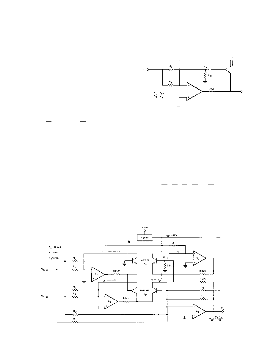
FOUR-QUADRANT MULTIPLIER
A simplified schematic for a four-quadrant log-antilog multiplier
is shown in Figure 5. Similar to the previously discussed one-
quadrant multiplier, the circuit makes I
O
= I
1
I
2
/I
3
. The two
input currents, I
1
and I
2
, are each offset in the positive direction.
This positive offset is then subtracted out at the output stage.
Assuming ideal op amps, the currents are:
I
V
R
V
R
I
V
R
V
R
X
R
Y
R
1
1
2
2
1
2
=
+
=
+
,
(11)
I
V
R
V
R
V
R
V
R
I
V
R
O
X
Y
R
O
O
R
=
+
+
+
=
1
1
2
3
2
,
From I
O
= I
1
I
2
/I
3
, the output voltage will be:
V
O
=
R
O
R
2
R
1
2
V
X
V
Y
V
R
(12)
Figure 5. Four-Quadrant Multiplier
MAT02
≠9≠
REV. E
Collector current range is the key design decision. The inher-
ently low r
BE
of the MAT02 allows the use of a relatively high
collector current. For input scaling of
±10 V full-scale and using
a 10 V reference, we have a collector-current range for I
1
and I
2
of:
≠10
10
10
10
1
2
1
2
R
R
I
R
R
C
+
+
(13)
Practical values for R
1
and R
2
would range from 50 k
to
100 k
. Choosing an R
1
of 82 k
and R
2
of 62 k
provides a
collector current range of approximately 39
µA to 283 µA. An
R
O
of 108 k
will then make the output scale factor 1/10 and
V
O
= V
X
V
Y
/10. The output, as well as both inputs, are scaled for
±10 V full scale.
Linear error for this circuit is substantially improved by the
small correction voltage applied to the base of Q1 as shown in
Figure 5. Assuming an equal bulk emitter resistance for each
MAT02 transistor, then the error is nulled if:
(I
1
+ I
2
≠ I
3
≠ I
O
) r
BE
+
V
O
= 0
The currents are known from the previous discussion, and the
relationship needed is simply:
V
O
=
r
BE
R
O
V
O
(14)
The output voltage is attenuated by a factor of r
BE
/R
O
and ap-
plied to the base of Q1 to cancel the summation of voltage drops
due to r
BE
I
C
terms. This will make In (I
1
I
2
/I
3
I
O
) more nearly
zero which will thereby make I
O
= I
1
I
2
/I
3
a more accurate rela-
tionship. Linearity of better than 0.1% is readily achievable with
this circuit if the MAT02 pairs are carefully kept at the same
temperature.
Figure 6. Multifunction Converter
MULTIFUNCTION CONVERTER
The multifunction converter circuit provides an accurate means
of squaring, square rooting, and raising ratios to arbitrary pow-
ers. The excellent log conformity of the MAT02 allows a wide
range of exponents. The general transfer function is:
V
O
= V
Y
V
Z
V
X
m
(15)
V
X
, V
Y
, and V
Z
are input voltages and the exponent "m" has a
practical range of approximately 0.2 to 5. Inputs V
X
and V
Y
are
often taken from a fixed reference voltage. With a REF01 pro-
viding a precision 10 V to both V
X
and V
Y
, the transfer function
would simplify to:
V
O
= 10
V
Z
10
m
(16)
As with the multiplier/divider circuits, assume that the transistor
pairs have excellent matching and are at the same temperature.
The In I
SA
/I
SB
will then be zero. In the circuit of Figure 6, the
voltage drops across the base-emitter junctions of Q1 provide:
R
B
R
B
+ KR
A
V
A
=
kT
q
In
I
Z
I
X
(17)
I
Z
is V
Z
/R
1
and I
X
is V
X
/R
1
. Similarly, the relationship for Q2 is:
R
B
R
B
+ 1≠ K
(
)
R
A
V
A
=
kT
q
In
I
O
I
Y
(18)
I
O
is V
O
/R
O
and I
Y
is V
Y
/R
1
. These equations for Q1 and Q2 can
then be combined.
R
B
+ KR
A
R
B
+ 1≠ K
(
)
R
A
In
I
Z
I
X
= In
I
O
I
Y
(19)
MAT02
≠10≠
REV. E
Substituting in the voltage relationships and simplifying leads
to:
V
O
=
R
O
R
1
V
Y
V
Z
V
X
m
, where
(20)
m =
R
B
+ KR
A
R
B
+ 1≠ K
(
)
R
A
The factor "K" is a potentiometer position and varies from zero
to 1.0, so "m" ranges from R
B
/(R
A
+ R
B
) to (R
B
+ R
A
)/R
B
.
Practical values are 125
for R
B
and 500
for R
A
; these
values will provide an adjustment range of 0.2 to 5.0. A value
of 100 k
is recommended for the R
1
resistors assuming a full-
scale input range of 10 V. As with the one-quadrant
multiplier/divider circuit previously discussed, the V
X
, V
Y
, and
V
Z
inputs must all be positive.
The op amps should have the lowest possible input offsets. The
OP07 is recommended for most applications, although such
programmable micropower op amps as the OP193/OP293 offer
advantages in low-power or single-supply circuits. The micro-
power op amps also have very low input bias-current drift, an
important advantage in log/antilog circuits. External offset
nulling may be needed, particularly for applications requiring a
wide dynamic range. Frequency compensating capacitors, on
the order of 50 pF, may be required for A
2
and A
3
. Amplifier
A
1
is likely to need a larger capacitor, typically 0.0047
µF, to
assure stability.
Accuracy is limited at the higher input levels by bulk emitter
resistance, but this is much lower for the MAT02 than for other
transistor pairs. Accuracy at the lower signal levels primarily
depends on the op amp offsets. Accuracies of better than 1%
are readily achievable with this circuit configuration and can be
better than
±0.1% over a limited operating range.
FAST LOGARITHMIC AMPLIFIER
The circuit of Figure 7 is a modification of a standard logarith-
mic amplifier configuration. Running the MAT02 at 2.5 mA
per side (full-scale) allows a fast response with wide dynamic
range. The circuit has a 7 decade current range, a 5 decade
voltage range, and is capable of 2.5
µs settling time to 1% with
a 1 V to 10 V step.
The output follows the equation:
V
O
=
R
3
+ R
2
R
2
kT
q
In
V
REF
V
IN
(21)
The output is inverted with respect to the input, and is nomi-
nally ≠1 V/decade using the component values indicated.
Figure 7. Fast Logarithmic Amplifier
LOW-NOISE 1000 AMPLIFIER
The MAT02 noise voltage is exceptionally low, only 1 nV/
Hz
at 10 Hz when operated over a collector current range of 1 mA
to 4 mA. A single-ended
◊1000 amplifier that takes advantage of
this low MAT02 noise level is shown in Figure 8. In addition to
low noise, the amplifier has very low drift and high CMRR. An
OP184 is used for the second stage to obtain good speed with
minimal power consumption. Small-signal bandwidth is 4.0
MHz, slew rate is 2.4 V/
µs, and total supply current is approxi-
mately 2.25 mA.
Figure 8. Low-Noise, Single-Ended
◊ 1000 Amplifier

MAT02
≠11≠
REV. E
Transistors Q2 and Q3 form a 2 mA current source (0.65 V/
330
~ 2 mA). Each collector of Q1 operates at 1 mA. The
OP184 inputs are 3 V below the positive supply voltage (R
L
I
C
~ 3 V). Input stage gain is g
m
R
L
, which is approximately 100
when operating at I
C
of 1 mA with R
L
of 3 k
. Since the
OP184 has a minimum open-loop gain of 500,000, total
open-loop gain for the composite amplifier is over 50 million.
Even at closed-loop gain of 1000, the gain error due to finite
open-loop gain will be negligible. The OP184 features excellent
symmetry of slew-rate and very linear gain. Signal distortion is
minimal.
Dynamic range of this amplifier is excellent; the OP184 has an
output voltage swing of
±14.8 V with a ±15 V supply.
Input characteristics are outstanding. The MAT02F has offset
voltage of less than 150
µV at 25∞C and a maximum offset drift
of 1
µV/∞C. Nulling the offset will further reduce offset drift.
This can be accomplished by slightly unbalancing the collector
load resistors. This adjustment will reduce the drift to less than
0.1
µV/∞C.
Input bias current is relatively low due to the high current gain
of the MAT02. The minimum
of 400 at 1 mA for the
MAT02F implies an input bias current of approximately 2.5
µA.
This circuit should be used with signals having relatively low
source impedance. A high source impedance will degrade offset
and noise performance.
This circuit configuration provides exceptionally low input noise
voltage and low drift. Noise can be reduced even further by
raising the collector currents from 1 mA to 3 mA, but power
consumption is then increased.
MAT02
≠12≠
REV. E
C00283≠0≠4/02(E)
PRINTED IN U.S.A.
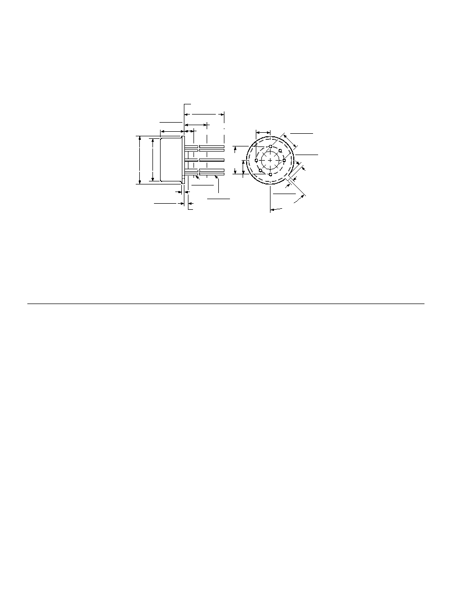
OUTLINE DIMENSION
Dimensions shown in inches and (mm).
6-Lead Metal Can
(TO-78)
0.250 (6.35) MIN
0.750 (19.05)
0.500 (12.70)
0.185 (4.70)
0.165 (4.19)
REFERENCE PLANE
0.050 (1.27) MAX
0.019 (0.48)
0.016 (0.41)
0.021 (0.53)
0.016 (0.41)
0.045 (1.14)
0.010 (0.25)
0.040 (1.02) MAX
BASE AND SEATING PLANE
0.335 (8.51)
0.305 (7.75)
0.370 (9.40)
0.335 (8.51)
0.034 (0.86)
0.027 (0.69)
0.045 (1.14)
0.027 (0.69)
0.160 (4.06)
0.110 (2.79)
0.100 (2.54) BSC
5
2
6
4
3
1
0.200
(5.08)
BSC
0.100
(2.54)
BSC
45
∞ BSC
Revision History
Location
Page
4/02--Data Sheet changed from REV. D to REV. E.
Changes to ORDERING GUIDE . . . . . . . . . . . . . . . . . . . . . . . . . . . . . . . . . . . . . . . . . . . . . . . . . . . . . . . . . . . . . . . . . . . . . . . . . . . 3
1/02--Data Sheet changed from REV. C to REV. D.
Edits to FEATURES . . . . . . . . . . . . . . . . . . . . . . . . . . . . . . . . . . . . . . . . . . . . . . . . . . . . . . . . . . . . . . . . . . . . . . . . . . . . . . . . . . . . . 1
Edits to ABSOLUTE MAXIMUM RATINGS . . . . . . . . . . . . . . . . . . . . . . . . . . . . . . . . . . . . . . . . . . . . . . . . . . . . . . . . . . . . . . . . . 1
Edits to ORDERING GUIDE . . . . . . . . . . . . . . . . . . . . . . . . . . . . . . . . . . . . . . . . . . . . . . . . . . . . . . . . . . . . . . . . . . . . . . . . . . . . . . 1
Deleted ELECTRICAL CHARACTERISTICS . . . . . . . . . . . . . . . . . . . . . . . . . . . . . . . . . . . . . . . . . . . . . . . . . . . . . . . . . . . . . . . . 3
Deleted WAFER TEST LIMITS . . . . . . . . . . . . . . . . . . . . . . . . . . . . . . . . . . . . . . . . . . . . . . . . . . . . . . . . . . . . . . . . . . . . . . . . . . . 4
Deleted TYPICAL ELECTRICAL CHARACTERISTICS . . . . . . . . . . . . . . . . . . . . . . . . . . . . . . . . . . . . . . . . . . . . . . . . . . . . . . . 4
Deleted DICE CHARACTERISTICS . . . . . . . . . . . . . . . . . . . . . . . . . . . . . . . . . . . . . . . . . . . . . . . . . . . . . . . . . . . . . . . . . . . . . . . 4
Edits to ABSOLUTE MAXIMUM RATINGS . . . . . . . . . . . . . . . . . . . . . . . . . . . . . . . . . . . . . . . . . . . . . . . . . . . . . . . . . . . . . . . . . 4
Edits to text . . . . . . . . . . . . . . . . . . . . . . . . . . . . . . . . . . . . . . . . . . . . . . . . . . . . . . . . . . . . . . . . . . . . . . . . . . . . . . . . . . . . . . . . . . . 12
Updated Figures . . . . . . . . . . . . . . . . . . . . . . . . . . . . . . . . . . . . . . . . . . . . . . . . . . . . . . . . . . . . . . . . . . . . . . . . . . . . . . . . . . . . . . . 12