 | –≠–ª–µ–∫—Ç—Ä–æ–Ω–Ω—ã–π –∫–æ–º–ø–æ–Ω–µ–Ω—Ç: OP177FS | –°–∫–∞—á–∞—Ç—å:  PDF PDF  ZIP ZIP |

PIN CONNECTIONS
REV. B
Information furnished by Analog Devices is believed to be accurate and
reliable. However, no responsibility is assumed by Analog Devices for its
use, nor for any infringements of patents or other rights of third parties
which may result from its use. No license is granted by implication or
otherwise under any patent or patent rights of Analog Devices.
a
Ultraprecision
Operational Amplifier
OP177
© Analog Devices, Inc., 1995
One Technology Way, P.O. Box 9106, Norwood, MA 02062-9106, U.S.A.
Tel: 617/329-4700
Fax: 617/326-8703
FEATURES
Ultralow Offset Voltage:
T
A
= +25 C: 10 V max
≠55 C
T
A
+125 C: 20 V max
Outstanding Offset Voltage Drift: 0.1 V/ C max
Excellent Open-Loop Gain and Gain Linearity:
12 V/ V typ
CMRR: 130 dB min
PSRR: 120 dB min
Low Supply Current: 2.0 mA max
Fits Industry Standard Precision Op Amp Sockets
(OP07/OP77)
GENERAL DESCRIPTION
The OP177 features the highest precision performance of any
op amp currently available. Offset voltage of the OP177 is only
10
µ
V max at room temperature and 20
µ
V max over the full
military temperature range of ≠55
∞
C to +125
∞
C. The ultralow
V
OS
of the OP177, combines with its exceptional offset voltage
drift (TCV
OS
) of 0.1
µ
V/
∞
C max, to eliminate the need for
external V
OS
adjustment and increases system accuracy over
temperature.
The OP177's open-loop gain of 12 V/
µ
V is maintained over the
full
±
10 V output range. CMRR of 130 dB min, PSRR of
120 dB min, and maximum supply current of 2 mA are just a
few examples of the excellent performance of this operational
amplifier. The OP177's combination of outstanding specifications
insure accurate performance in high closed-loop gain applications.
This low noise bipolar input op amp is also a cost effective
alternative to chopper-stabilized amplifiers. The OP177 provides
chopper-type performance without the usual problems of high
noise, low frequency chopper spikes, large physical size, limited
common-mode input voltage range, and bulky external storage
capacitors.
The OP177 is offered in both the ≠55
∞
C to +125
∞
C military,
and the ≠40
∞
C to +85
∞
C extended industrial temperature
ranges. This product is available in 8-pin ceramic and epoxy
DIPs, as well as the space saving 8-pin Small-Outline (SO) and
the Leadless Chip Carrier (LCC) packages.
Figure 1. Simplified Schematic
Epoxy Mini-DIP
(P Suffix)
8-Pin Hermetic DIP
(Z-Suffix)
8-Pin SO
(S-Suffix)
NC = NO CONNECT
OP177BRC/883
LCC (RC Suffix)
NC = NO CONNECT

OP177A
OP177B
Parameter
Symbol
Conditions
Min
Typ
Max
Min
Typ
Max
Units
Input Offset Voltage
V
OS
4
10
10
25
µ
V
Long-Term Input Offset Voltage Stability
V
OS
/Time
(Note 1)
0.2
0.2
µ
V/Mo
Input Offset Current
I
OS
0.3
1.0
0.3
1.5
nA
Input Bias Current
I
B
≠0.2
1.5
≠0.2
2.0
nA
Input Noise Voltage
e
n
f
o
= 1 Hz to 100 Hz
2
118
150
118
150
nV
rms
Input Noise Current
i
n
f
o
= 1 Hz to 100 Hz
2
3
8
3
8
pA
rms
Input Resistance Differential-Mode
R
IN
(Note 3)
26
45
26
45
M
Input Resistance Common-Mode
R
INCM
200
200
G
Input Voltage Range
IVR
(Note 4)
±
13
±
14
±
13
±
14
V
Common-Mode Rejection Ratio
CMRR
V
CM
=
±
13 V
130
140
130
140
dB
Power Supply Rejection Ratio
PSRR
V
S
=
±
3 V to
±
18 V
120
125
115
125
dB
Large Signal Voltage Gain
A
VO
R
L
2 k
, V
O
=
±
10 V
5
5000
12000
5000
12000
V/mV
Output Voltage Swing
V
O
R
L
10 k
±
13.5
±
14.0
±
13.5
±
14.0
V
R
L
2 k
±
12.5
±
13.0
±
12.5
±
13.0
V
R
L
1 k
±
12.0
±
12.5
±
12.0
±
12.5
V
Slew Rate
SR
R
L
2 k
2
0.1
0.3
0.1
0.3
V/
µ
s
Closed-Loop Bandwidth
BW
A
VCL
= +1
2
0.4
0.6
0.4
0.6
MHz
Open-Loop Output Resistance
R
O
60
60
Power Consumption
P
D
V
S
=
±
15 V, No Load
50
60
50
60
mW
V
S
=
±
3 V, No Load
3.5
4.5
3.5
4.5
mW
Supply Current
I
SY
V
S
=
±
15 V, No Load
1.6
2.0
1.6
2.0
mA
Offset Adjustment Range
Rp = 20 k
±
3
±
3
mV
NOTES
1
Long-Term Input Offset Voltage Stability refers to the averaged trend line of V
OS
vs. Time over extended periods after the first 30 days of operation. Excluding the
initial hour of operation, changes in V
OS
during the first 30 operating days are typically less than 2.0
µ
V.
2
Sample tested.
3
Guaranteed by design.
4
Guaranteed by CMRR test condition.
5
To insure high open-loop gain throughout the
±
10 V output range, A
VO
is tested at ≠10 V
V
O
0 V, 0 V
V
O
+10 V, and ≠10 V
V
O
+10 V.
Specifications subject to change without notice.
REV. B
≠2≠
OP177≠SPECIFICATIONS
ELECTRICAL CHARACTERISTICS
(@ V
S
= 15 V, T
A
= +25 C, unless otherwise noted)
ELECTRICAL CHARACTERISTICS
OP177A
OP177B
Parameter
Symbol
Conditions
Min
Typ
Max
Min
Typ
Max
Units
Input Offset Voltage
V
OS
10
20
25
55
µ
V
Average Input Offset Voltage Drift
TCV
OS
(Note 1)
0.03
0.1
0.1
0.3
µ
V/
∞
C
Input Offset Current
I
OS
0.5
1.5
0.5
2.0
nA
Average Input Offset Current Drift
TCI
OS
(Note 2)
1.5
25
1.5
25
pA/
∞
C
Input Bias Current
I
B
≠0.2
2.4
4
≠0.2
2.4
4
nA
Average Input Bias Current Drift
TCI
B
(Note 2)
8
25
8
25
pA/
∞
C
Input Voltage Range
IVR
(Note 3)
±
13
±
13.5
±
13
±
13.5
V
Common-Mode Rejection Ratio
CMRR
V
CM
=
±
13 V
120
140
120
140
dB
Power Supply Rejection Ratio
PSRR
V
S
=
±
3 V to
±
18 V
120
125
110
120
dB
Large-Signal Voltage Gain
A
VO
R
L
2 k
, V
O
=
±
10 V
4
2000
6000
2000
6000
V/mV
Output Voltage Swing
V
O
R
L
2 k
±
12
±
13.0
±
12
±
13.0
V
Power Consumption
P
D
V
S
=
±
15 V, No Load
60
75
60
75
mW
Supply Current
I
SY
V
S
=
±
15 V, No Load
2.0
2.5
2.0
2.5
mA
NOTES
1
TCV
OS
is 100% tested.
2
Guaranteed by endpoint limits.
3
Guaranteed by CMRR test condition.
4
To insure high open-loop gain throughout the
±
10 V output range, A
VO
is tested at ≠10 V
V
O
0 V, 0 V
V
O
+10 V, and ≠10 V
V
O
+10 V.
Specifications subject to change without notice.
(@ V
S
= 15 V, ≠55
∞
C
T
A
+125 C, unless otherwise noted)

OP177
REV. B
≠3≠
OP177E
OP177F
OP177G
Parameter
Symbol
Conditions
Min
Typ
Max
Min
Typ
Max
Min
Typ
Max
Units
Input Offset Voltage
V
OS
4
10
10
25
20
60
µ
V
Long-Term Input Offset
Voltage Stability
V
OS
/Time
(Note 1)
0.2
0.3
0.4
µ
V/Mo
Input Offset Current
I
OS
0.3
1.0
0.3
1.5
0.3
2.8
nA
Input Bias Current
I
B
≠0.2
1.0
1.5
≠0.2
1.2
2.0
≠0.2
1.2
2.8
nA
Input Noise Voltage
e
n
f
o
= 1 Hz to 100 Hz
2
118
150
118
150
118
150
nV
rms
Input Noise Current
i
n
f
o
= 1 Hz to 100 Hz
2
3
8
3
8
3
8
pA
rms
Input Resistance
Differential-Mode
R
IN
(Note 3)
26
45
26
45
18.5
45
M
Input Resistance
Common-Mode
R
INCM
200
200
200
G
Input Voltage Range
IVR
(Note 4)
±
13
±
14
±
13
±
14
±
13
±
14
V
Common-Mode
Rejection Ratio
CMRR
V
CM
=
±
13 V
130
140
130
140
115
140
dB
Power Supply
Rejection Ratio
PSRR
V
S
=
±
3 V to
±
18 V
120
125
115
125
110
120
dB
Large Signal
R
L
2 k
,
Voltage Gain
A
VO
V
O
=
±
10 V
5
5000
12000
5000
12000
2000
6000
V/mV
Output Voltage
Swing
V
O
R
L
10 k
±
13.5
±
14.0
±
13.5
±
14.0
±
13.5
±
14.0
V
R
L
2 k
±
12.5
±
13.0
±
12.5
±
13.0
±
12.5
±
13.0
V
R
L
1 k
±
12.0
±
12.5
±
12.0
±
12.5
±
12.0
±
12.5
V
Slew Rate
SR
R
L
2 k
2
0.1
0.3
0.1
0.3
0.1
0.3
V/
µ
s
Closed-Loop
Bandwidth
BW
A
VCL
= +1
2
0.4
0.6
0.4
0.6
0.4
0.6
MHz
Open-Loop Output
Resistance
R
O
60
60
60
Power Consumption
P
D
V
S
=
±
15 V, No Load
50
60
50
60
50
60
mW
V
S
=
±
3 V, No Load
3.5
4.5
3.5
4.5
3.5
4.5
mW
Supply Current
I
SY
V
S
=
±
15 V, No Load
1.6
2.0
1.6
2.0
1.6
2.0
mA
Offset Adjustment
Range
R
P
= 20 k
±
3
±
3
±
3
mV
NOTES
1
Long-Term Input Offset Voltage Stability refers to the averaged trend line of V
OS
vs. time over extended periods after the first 30 days of operation. Excluding the ini-
tial hour of operation, changes in V
OS
during the first 30 operating days are typically less than 2.0
µ
V.
2
Sample tested.
3
Guaranteed by design.
4
Guaranteed by CMRR test condition.
5
To insure high open-loop gain throughout the
±
10 V output range, A
VO
is tested at ≠10 V
V
O
0 V, 0 V
V
O
+10 V, and ≠10 V
V
O
+10 V.
Specifications subject to change without notice.
ELECTRICAL CHARACTERISTICS
(@ V
S
= 15 V, T
A
= +25 C, unless otherwise noted)

OP177≠SPECIFICATIONS
REV. B
≠4≠
ELECTRICAL CHARACTERISTICS
OP177E
OP177F
OP177G
Parameter
Symbol
Conditions
Min
Typ
Max
Min
Typ
Max
Min
Typ
Max
Units
Input Offset Voltage
V
OS
10
20
15
40
20
100
µ
V
Average Input Offset
Voltage Drift
TCV
OS
(Note 1)
0.03
0.1
0.1
0.3
0.7
1.2
µ
V/
∞
C
Input Offset Current
I
OS
0.5
1.5
0.5
2.2
0.5
4.5
nA
Average Input Offset
Current Drift
TCI
OS
(Note 2)
1.5
25
1.5
40
1.5
85
pA/
∞
C
Input Bias Current
I
B
≠0.2
2.4
4
≠0.2
2.4
4
2.4
±
6.0
nA
Average Input Bias
Current Drift
TCI
B
(Note 2)
8
25
8
40
15
60
pA/
∞
C
Input Voltage Range
IVR
(Note 3)
±
13
±
13.5
±
13
±
13.5
±
13.0
±
13.5
V
Common-Mode
Rejection Ratio
CMRR
V
CM
=
±
13 V
120
140
120
140
110
140
dB
Power Supply Rejection
Ratio
PSRR
V
S
=
±
3 V to
±
18 V
120
125
110
120
106
115
dB
Large-Signal
Voltage Gain
A
VO
R
L
2 k
, V
O
=
±
10 V
4
2000
6000
2000
6000
1000
4000
V/mV
Output Voltage Swing
V
O
R
L
2 k
±
12
±
13.0
±
12
±
13.0
±
12.0
±
13.0
V
Power Consumption
P
D
V
S
=
±
15 V, No Load
60
75
60
75
60
75
mW
Supply Current
I
SY
V
S
=
±
15 V, No Load
2.0
2.5
2.0
2.5
2.0
2.5
mA
NOTES
1
OP177E: TCV
OS
is 100% tested.
2
Guaranteed by endpoint limits.
3
Guaranteed by CMRR test condition.
4
To insure high open-loop gain throughout the
±
10 V output range, A
VO
is tested at ≠10 V
V
O
0 V, 0 V
V
O
+10 V, and ≠10 V
V
O
+10 V.
Specifications subject to change without notice.
Figure 2. Typical Offset Voltage Test Circuit
Figure 3. Optional Offset Nulling Circuit
(@ V
S
= 15 V, ≠40
∞
C
T
A
+85 C, unless otherwise noted)

OP177
REV. B
≠5≠
ABSOLUTE MAXIMUM RATINGS
Supply Voltage . . . . . . . . . . . . . . . . . . . . . . . . . . . . . . .
±
22 V
Internal Power Dissipation
1
. . . . . . . . . . . . . . . . . . . 500 mW
Differential Input Voltage . . . . . . . . . . . . . . . . . . . . . .
±
30 V
Input Voltage . . . . . . . . . . . . . . . . . . . . . . . . . . . . . . . .
±
22 V
Output Short-Circuit Duration . . . . . . . . . . . . . . . . Indefinite
Storage Temperature Range
Z and RC Packages . . . . . . . . . . . . . . . . . ≠65
∞
C to +150
∞
C
S, P Package . . . . . . . . . . . . . . . . . . . . . . ≠65
∞
C to +125
∞
C
Operating Temperature Range
OP177A, OP177B . . . . . . . . . . . . . . . . . ≠55
∞
C to +125
∞
C
OP177E, OP177F, OP177G . . . . . . . . . . ≠40
∞
C to +85
∞
C
Lead Temperature Range (Soldering, 60 sec) . . . . . . +300
∞
C
DICE Junction Temperature (T
J
) . . . . . . . ≠65
∞
C to +150
∞
C
Package Type
JA
2
JC
Units
8-Pin Hermetic DIP (Z)
148
16
∞
C/W
8-Pin Plastic DIP (P)
103
43
∞
C/W
20-Contact LCC (RC)
98
38
∞
C/W
8-Pin SO (S)
158
43
∞
C/W
NOTES
1
For supply voltages less than
±
22 V, the absolute maximum input voltage is equal
to the supply voltage.
2
JA
is specified for worst case mounting conditions, i.e.,
JA
is specified for
device in socket for cerdip, P-DIP, and LCC packages;
JA
is specified for
device soldered to printed circuit board for SO package.
Figure 4. Burn-In Circuit
ORDERING GUIDE
Temperature
Package
Package
Model
Range
Description
Option
OP177AZ
≠55
∞
C to +125
∞
C 8-Pin Cerdip
Q-8
OP177BZ
≠55
∞
C to +125
∞
C 8-Pin Cerdip
Q-8
OP177EZ
≠40
∞
C to +85
∞
C
8-Pin Cerdip
Q-8
OP177FZ
≠40
∞
C to +85
∞
C
8-Pin Cerdip
Q-8
OP177GZ
≠40
∞
C to +85
∞
C
8-Pin Cerdip
Q-8
OP177FP
≠40
∞
C to +85
∞
C
8-Pin Plastic DIP N-8
OP177GP
≠40
∞
C to +85
∞
C
8-Pin Plastic DIP N-8
OP177BRC/883 ≠55
∞
C to +125
∞
C 20-Pin LCC
E-20A
OP177FS
≠40
∞
C to +85
∞
C
8-Pin SO
SO-8
OP177GS
≠40
∞
C to +85
∞
C
8-Pin SO
SO-8

OP177≠Typical Performance Characteristics
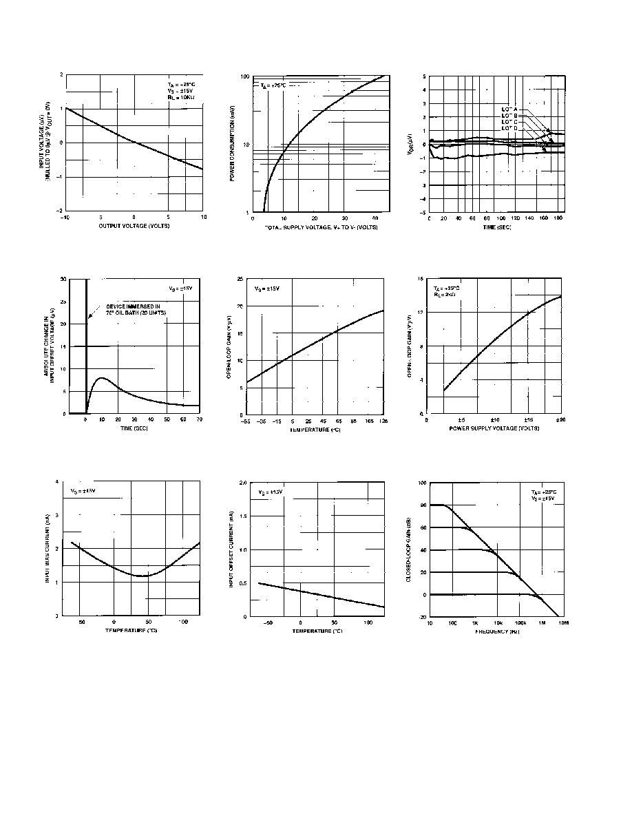
Figure 6. Power Consumption vs.
Power Supply
Figure 9. Open-Loop Gain
vs. Temperature
Figure 12. Input Offset Current
vs. Temperature
Figure 7. Warm-Up V
OS
Drift
(Normalized) Z Package
Figure 10. Open-Loop Gain vs.
Power Supply Voltage
Figure 13. Closed-Loop Response
for Various Gain Configurations
Figure 5. Gain Linearity (Input
Voltage vs. Output Voltage)
Figure 8. Offset Voltage Change
Due to Thermal Shock
Figure 11. Input Bias Current
vs. Temperature

OP177
REV. B
≠7≠
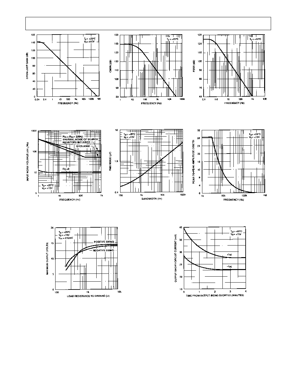
Figure 15. CMRR vs. Frequency
Figure 18. Input Wideband Noise
vs. Bandwidth (0.1 Hz to
Frequency Indicated)
Figure 16. PSRR vs. Frequency
Figure 19. Maximum Output Swing
vs. Frequency
Figure 14. Open-Loop
Frequency Response
Figure 17. Total Input Noise
Voltage vs. Frequency
Figure 20. Maximum Output Voltage
vs. Load Resistance
Figure 21. Output Short Circuit
Current vs. Time

OP177
APPLICATIONS INFORMATION
Gain Linearity
The actual open-loop gain of most monolithic op amps varies at
different output voltages. This nonlinearity causes errors in high
closed-loop gain circuits.
It is important to know that the manufacturer's A
VO
specifi-
cation is only a part of the solution, since all automated testers
use endpoint testing and, therefore, only show the average gain.
For example, Figure 22 shows a typical precision op amp with a
respectable open-loop gain of 650 V/mV. However, the gain is
not constant through the output voltage range, causing
nonlinear errors. An ideal op amp would show a horizontal
scope trace.
Figure 22. Typical Precision Op Amp
Figure 23. OP177's Output Gain Linearity Trace
Figure 24. Open-Loop Gain Linearity Test Circuit
Figure 23 shows the OP177's output gain linearity trace with its
truly impressive average A
VO
of 12000 V/mV. The output trace
is virtually horizontal at all points, assuring extremely high gain
accuracy. PMI also performs additional testing to insure
consistent high open-loop gain at various output voltages.
Figure 24 is a simple open-loop gain test circuit for your own
evaluation.
THERMOCOUPLE AMPLIFIER WITH COLD-JUNCTION
COMPENSATION
An example of a precision circuit is a thermocouple amplifier
that must amplify very low level signals accurately without
introducing linearity and offset errors to the circuit. In this
circuit, an S-type thermocouple, which has a Seebeck coefficient
of 10.3 µV/∞C, produces 10.3 mV of output voltage at a
temperature of 1,000∞C. The amplifier gain is set at 973.16.
Thus, it will produce an output voltage of 10.024 V. Extended
temperature ranges to beyond 1,500∞C can be accomplished by
reducing the amplifier gain. The circuit uses a low-cost diode to
sense the temperature at the terminating junctions and in turn
compensates for any ambient temperature change. The OP177,
with its high open-loop gain, plus low offset voltage and drift
combines to yield a very precision temperature sensing circuit. Cir-
cuit values for other thermocouple types are shown in Table I.
Table I.
Thermo-
Seebeck
couple Type Coefficient
R1
R2
R7
R9
K
39.2 µV/∞C
110
5.76 k
102 k
269 k
J
50.2 µV/∞C
100
4.02 k
80.6 k
200 k
S
10.3 µV/∞C
100
20.5 k
392 k
1.07 M
Figure 25. Thermocouple Amplifier with Cold Junction
Compensation
PRECISION HIGH GAIN DIFFERENTIAL AMPLIFIER
The high gain, gain linearity, CMRR, and low TCV
OS
of the
OP177 make it possible to obtain performance not previously
available in single stage, very high-gain amplifier applications.
See Figure 26.
For best CMR,
R1
R2
must equal
R3
R4
. In this example, with a
10 mV differential signal, the maximum errors are as listed in
Table II.

OP177
Figure 26. Precision High Gain Differential Amplifier
Table II. High Gain Differential Amp Performance
Type
Amount
Common-Mode Voltage
0.1%/V
Gain Linearity, Worst Case
0.02%
TCV
OS
0.0003%/∞C
TCI
OS
0.008%/∞C
ISOLATING LARGE CAPACITIVE LOADS
The circuit in Figure 27 reduces maximum slew-rate but allows
driving capacitive loads of any size without instability. Because
the 100
resistor is inside the feedback loop, its effect on
output impedance is reduced to insignificance by the high open-
loop gain of the OP177.
Figure 27. Isolating Capacitive Loads
Figure 28. Bilateral Current Source
Figure 29. Precision Absolute Value Amplifier

OP177
REV. B
≠10≠
BILATERAL CURRENT SOURCE
The current sources shown in Figure 28 will supply both
positive and negative current into a grounded load.
Note that Z
O
=
R5
R4
R2
+
1
R5
+
R4
R2
≠
R3
R1
and that for Z
O
to be infinite,
R5
+
R4
R2
must
=
R3
R1
PRECISION ABSOLUTE VALUE AMPLIFIER
The high gain and low TCV
OS
assure accurate operation with
inputs from microvolts to volts. In this circuit, the signal always
appears as a common-mode signal to the op amps. The
OP177E CMRR of 140 dB assures errors of less than 1 ppm.
See Figure 29.
PRECISION POSITIVE PEAK DETECTOR
In Figure 30, the C
H
must be of polystyrene, Teflon*, or
polyethylene to minimize dielectric absorption and leakage. The
droop rate is determined by the size of C
H
and the bias current
of the OP41.
PRECISION THRESHOLD DETECTOR/AMPLIFIER
In Figure 32, when V
IN
< V
TH
, amplifier output swings nega-
tive, reverse biasing diode D
1
. V
OUT
= V
TH
if R
L
=
. When
V
IN
V
TH
, the loop closes,
V
OUT
=
V
TH
+
V
IN
≠V
TH
(
)
1
+
R
F
R
S
C
C
is selected to smooth the response of the loop.
*Teflon is a registered trademark of the Dupont Company.
Figure 31. Precision Threshold Detector/Amplifier
Figure 30. Precision Positive Peak Detector

OP177
REV. B
≠11≠
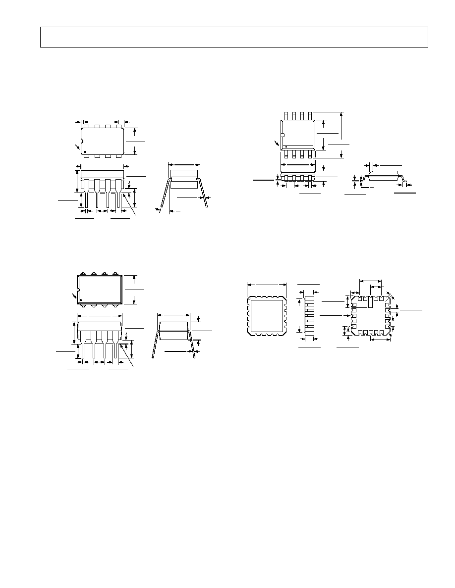
OUTLINE DIMENSIONS
Dimensions shown in inches and (mm).
8-Pin Cerdip
(Q-8)
0.320 (8.13)
0.290 (7.37)
0.015 (0.38)
0.008 (0.20)
15
∞
0
∞
0.005 (0.13) MIN
0.055 (1.4) MAX
1
PIN 1
4
5
8
0.310 (7.87)
0.220 (5.59)
0.405 (10.29) MAX
0.200
(5.08)
MAX
SEATING
PLANE
0.023 (0.58)
0.014 (0.36)
0.070 (1.78)
0.030 (0.76)
0.060 (1.52)
0.015 (0.38)
0.150
(3.81)
MIN
0.200 (5.08)
0.125 (3.18)
0.100
(2.54)
BSC
8-Pin Plastic DIP
(N-8)
PIN 1
0.280 (7.11)
0.240 (6.10)
4
5
8
1
SEATING
PLANE
0.060 (1.52)
0.015 (0.38)
0.130
(3.30)
MIN
0.210
(5.33)
MAX
0.160 (4.06)
0.115 (2.93)
0.430 (10.92)
0.348 (8.84)
0.022 (0.558)
0.014 (0.356)
0.070 (1.77)
0.045 (1.15)
0.100
(2.54)
BSC
0.325 (8.25)
0.300 (7.62)
0.015 (0.381)
0.008 (0.204)
0.195 (4.95)
0.115 (2.93)
8-Pin SO
(SO-08)
0.0098 (0.25)
0.0075 (0.19)
0.0500 (1.27)
0.0160 (0.41)
8
∞
0
∞
0.0196 (0.50)
0.0099 (0.25)
x 45
∞
PIN 1
0.1574 (4.00)
0.1497 (3.80)
0.2440 (6.20)
0.2284 (5.80)
4
5
1
8
0.0192 (0.49)
0.0138 (0.35)
0.0500
(1.27)
BSC
0.0688 (1.75)
0.0532 (1.35)
0.0098 (0.25)
0.0040 (0.10)
0.1968 (5.00)
0.1890 (4.80)
20-Pin LCC
(E-20A)
TOP
VIEW
0.358 (9.09)
0.342 (8.69)
SQ
1
20
4
9
8
13
19
BOTTOM
VIEW
14
3
18
0.028 (0.71)
0.022 (0.56)
45
∞
TYP
0.015 (0.38)
MIN
0.055 (1.40)
0.045 (1.14)
0.050 (1.27)
BSC
0.075 (1.91)
REF
0.011 (0.28)
0.007 (0.18)
R TYP
0.095 (2.41)
0.075 (1.90)
0.100 (2.54) BSC
0.200 (5.08)
BSC
0.150 (3.81)
BSC
0.075
(1.91)
REF
0.358
(9.09)
MAX
SQ
0.100 (2.54)
0.064 (1.63)
0.088 (2.24)
0.054 (1.37)

C2087≠5≠11/95
PRINTED IN U.S.A.
≠12≠


