 | –≠–ª–µ–∫—Ç—Ä–æ–Ω–Ω—ã–π –∫–æ–º–ø–æ–Ω–µ–Ω—Ç: OP279GP | –°–∫–∞—á–∞—Ç—å:  PDF PDF  ZIP ZIP |

PIN CONFIGURATIONS
REV. F
Information furnished by Analog Devices is believed to be accurate and
reliable. However, no responsibility is assumed by Analog Devices for its
use, nor for any infringements of patents or other rights of third parties
which may result from its use. No license is granted by implication or
otherwise under any patent or patent rights of Analog Devices.
a
Rail-to-Rail High Output
Current Operational Amplifiers
OP179/OP279
GENERAL DESCRIPTION
The OP179 and OP279 are rail-to-rail, high output current,
single-supply amplifiers. They are designed for low voltage
applications that require either current or capacitive load drive
capability. The OP179/OP279 can sink and source currents of
±
60 mA (typical) and are stable with capacitive loads to 10 nF.
Applications that benefit from the high output current of the
OP179/OP279 include driving headphones, displays, transform-
ers and power transistors. The powerful output is combined with a
unique input stage that maintains very low distortion with
wide common-mode range, even in single supply designs.
The OP179/OP279 can be used as a buffer to provide much
greater drive capability than can usually be provided by CMOS
outputs. CMOS ASICs and DAC often have outputs that can
swing to both the positive supply and ground, but cannot drive
more than a few milliamps.
Bandwidth is typically 5 MHz and the slew rate is 3 V/
µ
s, mak-
ing these amplifiers well suited for single supply applications
that require audio bandwidths when used in high gain configu-
rations. Operation is guaranteed from voltages as low as 4.5 V,
up to 12 V.
Very good audio performance can be attained when using the
OP179/OP279 in +5 volt systems. THD is below 0.01% with a
600
load, and noise is a respectable 21 nV/
Hz. Supply cur-
rent is less than 3.5 mA per amplifier.
The single OP179 is available in the 5-lead SOT-23-5 package.
It is specified over the industrial (≠40
∞
C to +85
∞
C) temperature
range.
The OP279 is available in 8-lead plastic DIP, TSSOP and
SO-8 surface mount packages. They are specified over the
industrial (≠40
∞
C to +85
∞
C) temperature range.
8-Lead SOIC and TSSOP
SO-8 (R) and RU-8
1
2
3
4
8
7
6
5
OP279
IN A
V
+IN A
OUT B
IN B
V+
+IN B
OUT A
8-Lead Plastic DIP
(N-8)
OUT A
≠IN A
+IN A
≠V
+V
OUT B
≠IN B
+IN B
OP279
FEATURES
Rail-to-Rail Inputs and Outputs
High Output Current:
60 mA
Single Supply: +5 V to +12 V
Wide Bandwidth: 5 MHz
High Slew Rate: 3 V/ s
Low Distortion: 0.01%
Unity-Gain Stable
No Phase Reversal
Short Circuit Protected
Drives Capacitive Loads: 10 nF
APPLICATIONS
Multimedia
Telecom
DAA Transformer Driver
LCD Driver
Low Voltage Servo Control
Modems
FET Drivers
5-Lead SOT-23-5
(RT-5)
1
2
3
5
4
IN A
+IN A
V≠
OUT A
OP179
V+
One Technology Way, P.O. Box 9106, Norwood, MA 02062-9106, U.S.A.
Tel: 781/329-4700
World Wide Web Site: http://www.analog.com
Fax: 781/326-8703
© Analog Devices, Inc., 1999
ELECTRICAL SPECIFICATIONS
(@ V
S
= +5.0 V, V
CM
= 2.5 V, ≠40 C
T
A
+85 C unless otherwise noted)
Parameter
Symbol
Conditions
Min
Typ
Max
Units
INPUT CHARACTERISTICS
Offset Voltage
OP179
V
OS
V
OUT
= 2.5 V
±
5
mV
OP279
V
OS
V
OUT
= 2.5 V
±
4
mV
Input Bias Current
I
B
V
OUT
= 2.5 V, T
A
= +25
∞
C
±
300
nA
V
OUT
= 2.5 V
±
700
nA
Input Offset Current
I
OS
V
OUT
= 2.5 V, T
A
= +25
∞
C
±
50
nA
V
OUT
= 2.5 V
±
100
nA
Input Voltage Range
V
CM
0
5
V
Common-Mode Rejection Ratio
CMRR
V
CM
= 0 V to 5 V
56
66
dB
Large Signal Voltage Gain
A
VO
R
L
= 1 k
, 0.3 V
V
OUT
4.7 V
20
V/mV
Offset Voltage Drift
V
OS
/
T
4
µ
V/
∞
C
OUTPUT CHARACTERISTICS
Output Voltage High
V
OH
I
L
= 10 mA Source
+4.8
V
Output Voltage Low
V
OL
I
L
= 10 mA Sink, T
A
= +25
∞
C
75
mV
I
L
= 10 mA Sink
100
mV
Short Circuit Limit
I
SC
T
A
= +25
∞
C
±
40
mA
Output Impedance
Z
OUT
f = 1 MHz, A
V
= 1
22
POWER SUPPLY
Power Supply Rejection Ratio
PSRR
V
S
= +4.5 V to +12 V
70
88
dB
Supply Current/Amplifier
I
SY
V
OUT
= 2.5 V
3.5
mA
Supply Voltage Range
V
S
+4.5
+12
V
DYNAMIC PERFORMANCE
Slew Rate
SR
R
L
= 1 k
, 1 nF
3
V/
µ
s
Gain Bandwidth Product
GBP
5
MHz
Phase Margin
m
60
Degrees
Capacitive Load Drive
No Oscillation
10
nF
AUDIO PERFORMANCE
Total Harmonic Distortion
THD
0.01
%
Voltage Noise Density
e
n
f = 1 kHz
22
nV/
Hz
ELECTRICAL SPECIFICATIONS
(@ V
S
= 5.0 V, ≠40 C
T
A
+85 C unless otherwise noted)
Parameter
Symbol
Conditions
Min
Typ
Max
Units
INPUT CHARACTERISTICS
Offset Voltage
OP179
V
OS
V
OUT
= 0
±
5
mV
OP279
V
OS
V
OUT
= 0
±
4
mV
Input Bias Current
I
B
T
A
= +25
∞
C
±
300
nA
±
700
nA
Input Offset Current
I
OS
T
A
= +25
∞
C
±
50
nA
±
100
nA
Input Voltage Range
V
CM
≠5
+5
V
Common-Mode Rejection Ratio
CMRR
V
CM
= ≠5 V to +5 V
56
66
dB
Large Signal Voltage Gain
A
VO
R
L
= 1 k
, ≠4.7 V
V
OUT
4.7 V
20
V/mV
Offset Voltage Drift
V
OS
/
T
3
µ
V/
∞
C
OUTPUT CHARACTERISTICS
Output Voltage High
V
OH
I
L
= 10 mA Source
+4.8
V
Output Voltage Low
V
OL
I
L
= 10 mA Sink
≠4.85
V
Short Circuit Limit
I
SC
T
A
= +25
∞
C
±
50
mA
Open-Loop Output Impedance
Z
OUT
f = 1 MHz, A
V
= +1
22
POWER SUPPLY
Supply Current/Amplifier
I
SY
V
S
=
±
6 V, V
OUT
= 0 V
3.75
mA
DYNAMIC PERFORMANCE
Slew Rate
SR
R
L
= 1 k
, 1 nF
3
V/
µ
s
Full-Power Bandwidth
BW
p
1% Distortion
kHz
Gain Bandwidth Product
GBP
5
MHz
Phase Margin
m
69
Degrees
NOISE PERFORMANCE
Voltage Noise
e
n
p-p
0.1 Hz to 10 Hz
2
µ
V p-p
Voltage Noise Density
e
n
f = 1 kHz
22
nV/
Hz
Current Noise Density
i
n
1
pA/
Hz
Specifications subject to change without notice.
OP179/OP279≠SPECIFICATIONS
≠2≠
REV. F
OP179/OP279
≠3≠
REV. F
ABSOLUTE MAXIMUM RATINGS
Supply Voltage . . . . . . . . . . . . . . . . . . . . . . . . . . . . . . . . . +16 V
Input Voltage . . . . . . . . . . . . . . . . . . . . . . . . . . . . . . . . . . +16 V
Differential Input Voltage
1
. . . . . . . . . . . . . . . . . . . . . . . . .
±
1 V
Output Short-Circuit Duration to GND . . . . . . . . . . Indefinite
Storage Temperature Range
P, S, RT, RU Package . . . . . . . . . . . . . . . . ≠65
∞
C to +150
∞
C
Operating Temperature Range
OP179G/OP279G . . . . . . . . . . . . . . . . . . . . ≠40
∞
C to +85
∞
C
Junction Temperature Range
P, S, RT, RU Package . . . . . . . . . . . . . . . . ≠65
∞
C to +150
∞
C
Lead Temperature Range (Soldering, 60 sec) . . . . . . . +300
∞
C
CAUTION
ESD (electrostatic discharge) sensitive device. Electrostatic charges as high as 4000 V readily
accumulate on the human body and test equipment and can discharge without detection.
Although the OP179/OP279 features proprietary ESD protection circuitry, permanent damage
may occur on devices subjected to high energy electrostatic discharges. Therefore, proper ESD
precautions are recommended to avoid performance degradation or loss of functionality.
ORDERING GUIDE
Package
Temperature Range
Package Description
Package Option
Brand Code
OP179GRT
≠40
∞
C to +85
∞
C
5-Lead SOT-23
RT-5
A2G
OP279GP
≠40
∞
C to +85
∞
C
8-Lead Plastic DIP
N-8
OP279GS
≠40
∞
C to +85
∞
C
8-Lead SOIC
SO-8
OP279GRU
≠40
∞
C to +85
∞
C
8-Lead TSSOP
RU-8
WARNING!
ESD SENSITIVE DEVICE
Package Types
JA
2
JC
Unit
5-Lead SOT-23 (RT)
256
81
∞
C/W
8-Lead Plastic DIP (P)
103
43
∞
C/W
8-Lead SOIC (S)
158
43
∞
C/W
8-Lead TSSOP (RU)
240
43
∞
C/W
NOTES
1
The inputs are clamped with back-to-back diodes. If the differential input voltage
exceeds 1 volt, the input current should be limited to 5 mA.
2
JA
is specified for the worst case conditions, i.e.,
JA
is specified for device in socket
for P-DIP, packages;
JA
is specified for device soldered in circuit board for SOIC
packages.

OP179/OP279
≠4≠
REV. F
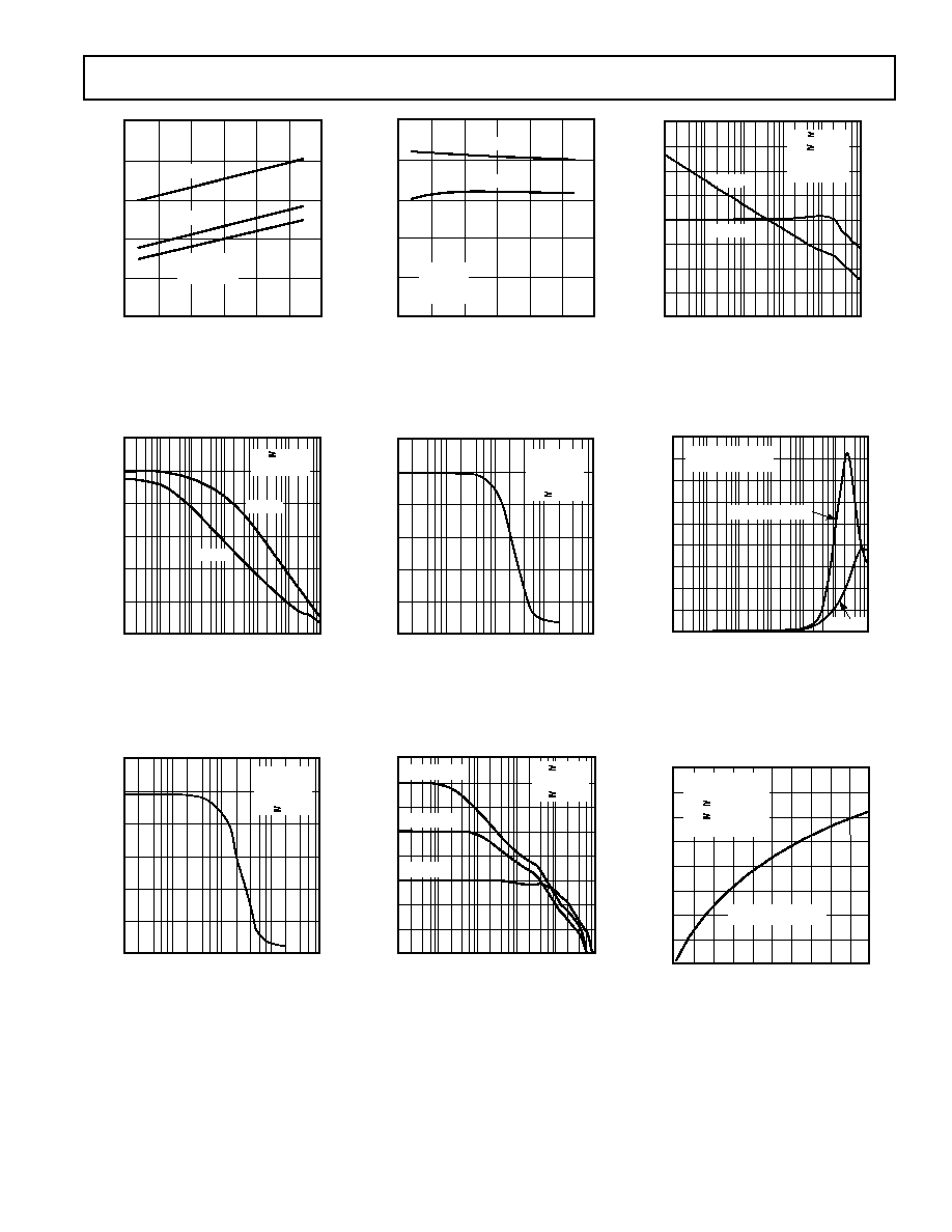
Typical Performance Graphs
160
0
2.5
40
20
≠2.5
80
60
100
120
140
1.5
0.5
≠0.5
≠1.5
INPUT OFFSET ≠ mV
UNITS
V
S
= +5V
T
A
= +25 C
620 x OP AMPS,
PDIP
Figure 1. Input Offset Distribution
COMMON-MODE VOLTAGE ≠ Volts
OFFSET VOLTAGE ≠ mV
3.0
0
5
1.5
0.5
1
1.0
0
2.5
2.0
4
3
2
V
S
= +5V
T
A
= +25 C
Figure 4. Offset Voltage vs.
Common-Mode Voltage
1000
0
100
600
200
≠25
400
≠50
800
75
50
25
0
TEMPERATURE ≠ C
R
L
= 2k
R
L
= 1k
OPEN-LOOP GAIN ≠ V/mV
V
S
= 15V
0.3 V
OUT
4.7V
Figure 7. Open-Loop Gain vs.
Temperature
V
S
= +5V
V
CM
= +2.5V
90
40
100
70
50
≠25
60
≠50
80
75
50
25
0
TEMPERATURE ≠ C
≠I
SC
SHORT CIRCUIT CURRENT ≠ mA
+I
SC
Figure 2. Short Circuit Current vs.
Temperature
V
S
= 5V
100
50
100
80
60
≠25
70
≠50
90
75
50
25
0
TEMPERATURE ≠ C
SHORT CIRCUIT CURRENT ≠ mA
≠I
SC
+I
SC
Figure 5. Short Circuit Current vs.
Temperature
5
0
100
3
1
≠25
2
≠50
4
75
50
25
0
TEMPERATURE ≠ C
SLEW RATE ≠ V/
s
V
S
= +5V
R
L
= 1k
C
L
= +1nF
+EDGE
≠EDGE
Figure 8. Slew Rate vs.
Temperature
400
≠400
5
≠200
≠300
1
0
0
≠100
100
200
300
4
3
2
+85 C
+25 C
COMMON-MODE VOLTAGE ≠ Volts
INPUT BIAS CURRENT ≠ nA
V
S
= +5V
≠40 C
Figure 3. Input Bias Current
vs. Common-Mode Voltage
COMMON-MODE VOLTAGE ≠ Volts
7
0
5
3
1
1
2
0
6
4
5
4
3
2
BANDWIDTH ≠ MHz
V
S
= +5V
T
A
= +25 C
Figure 6. Bandwidth vs.
Common-Mode Voltage
PHASE
GAIN
40
≠40
100
1k
10M
1M
100k
10k
60
80
100
≠20
0
20
90
≠90
135
180
225
≠45
0
45
FREQUENCY ≠ Hz
OPEN-LOOP GAIN ≠ dB
PHASE ≠ Degrees
120
270
V
S
2.5V
T
A
≠40 C
R
L
= 2k
Figure 9. Open-Loop Gain and
Phase vs. Frequency
OP179/OP279
≠5≠
REV. F
V
S
= +5V
V
CM
= +2.5V
6.5
4.0
100
5.5
4.5
≠25
5.0
≠50
6.0
75
50
25
0
TEMPERATURE ≠ C
SUPPLY CURRENT ≠ mA
V
S
= 6V
V
S
= 5V
Figure 10. Supply Current vs.
Temperature
FREQUENCY ≠ Hz
POWER SUPPLY REJECTION ≠ dB
120
60
0
10
100
10M
1M
100k
10k
1k
80
100
20
40
V
S
2.5V
T
A
= +25 C
≠PSRR
+PSRR
Figure 13. Power Supply Rejection vs.
Frequency
12
6
0
10k
10M
1M
100k
1k
4
2
8
10
FREQUENCY ≠ Hz
MAXIMUM OUTPUT SWING ≠ Volts
T
A
= +25 C
V
S
= 5V
A
VCL
= +1
R
L
1k
Figure 16. Maximum Output Swing
vs. Frequency
5
0
100
3
1
≠25
2
≠50
4
75
50
25
0
TEMPERATURE ≠ C
SLEW RATE ≠ V/
s
V
S
= 5V
R
L
= 1k
C
L
= +1nF
+EDGE
≠EDGE
Figure 11. Slew Rate vs. Temperature
6
3
0
10k
10M
1M
100k
1k
2
1
4
5
FREQUENCY ≠ Hz
MAXIMUM OUTPUT SWING ≠ Volts
T
A
= +25 C
V
S
= 2.5V
A
VCL
= +1
R
L
1k
Figure 14. Maximum Output
Swing vs. Frequency
50
10
≠30
1k
10k
100M
10M
1M
100k
20
30
40
≠20
≠10
0
FREQUENCY ≠ Hz
CLOSED-LOOP GAIN ≠ dB
A
VCL
= +100
A
VCL
= +10
A
VCL
= +1
V
S
2.5V
T
A
= +25 C
R
L
1k
Figure 17. Closed-Loop Gain vs.
Frequency
PHASE
GAIN
120
40
≠40
100
1k
10M
1M
100k
10k
60
80
100
≠20
0
20
270
90
≠90
135
180
225
≠45
0
45
FREQUENCY ≠ Hz
OPEN-LOOP GAIN ≠ dB
PHASE ≠ Degrees
V
S
2.5V
T
A
≠40 C
R
L
= 2k
C
L
= 500pF
Figure 12. Open-Loop Gain and
Phase vs. Frequency
180
160
140
120
100
80
60
40
20
0
10
100
10M
1M
100k
10k
1k
T
A
= +25 C
V
S
= 2.5V OR 5V
FREQUENCY ≠ Hz
IMPEDANCE ≠
A
VCL
= 1
A
VCL
= 10 OR 100
Figure 15. Closed-Loop Output
Impedance vs. Frequency
80
0
10k
20
10
0
40
30
50
60
70
8k
6k
4k
2k
LOAD CAPACITANCE ≠ pF
OVERSHOOT ≠ %
T
A
= +25 C
A
VCL
= +1
R
L
1k
V
S
2.5V
V
IN
= +100mV p-p
POSITIVE EDGE AND
NEGATIVE EDGE
Figure 18. Small Signal Overshoot
vs. Load Capacitance
OP179/OP279
≠6≠
REV. F
Typical Performance Graphs
THEORY OF OPERATION
The OP179/OP279 is the latest entry in Analog Devices' ex-
panding family of single-supply devices, designed for the multi-
media and telecom marketplaces. It is a high output current
drive, rail-to-rail input /output operational amplifier, powered
from a single +5 V supply. It is also intended for other low
supply voltage applications where low distortion and high out-
put current drive are needed. To combine the attributes of high
output current and low distortion in rail-to-rail input/output
operation, novel circuit design techniques are used.
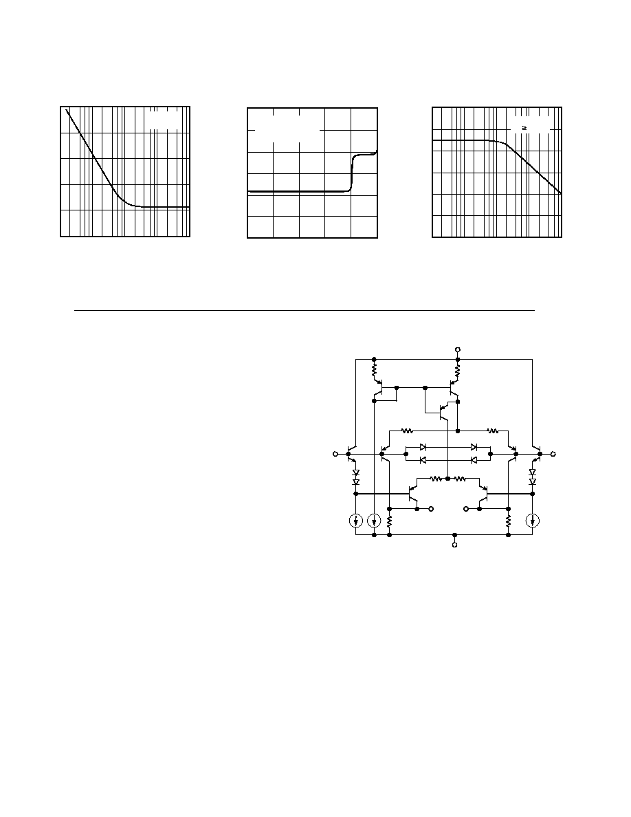
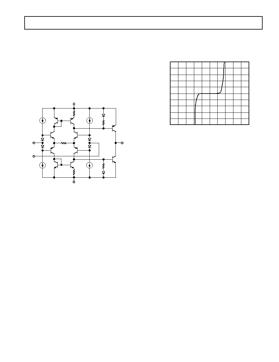
For example, Figure 1 illustrates a simplified equivalent circuit
for the OP179/OP279's input stage. It is comprised of two PNP
differential pairs, Q5-Q6 and Q7-Q8, operating in parallel, with
diode protection networks. Diode networks D5-D6 and D7-D8
serve to clamp the applied differential input voltage to the
OP179/OP279, thereby protecting the input transistors against
avalanche damage. The fundamental differences between these
two PNP gain stages are that the Q7-Q8 pair are normally OFF
and that their inputs are buffered from the operational amplifier
inputs by Q1-D1-D2 and Q9-D3-D4. Operation is best under-
stood as a function of the applied common-mode voltage:
When the inputs of the OP179/OP279 are biased midway be-
tween the supplies, the differential signal path gain is controlled
by the resistively loaded (via R7, R8) Q5-Q6. As the input
common-mode level is reduced toward the negative supply
(V
NEG
or GND), the input transistor current sources, I1 and I3,
are forced into saturation, thereby forcing the Q1-D1-D2 and
Q9-D3-D4 networks into cutoff; however, Q5-Q6 remain
active, providing input stage gain. On the other hand, when the
common-mode input voltage is increased toward the positive
supply, Q5-Q6 are driven into cutoff, Q3 is driven into satura-
tion, and Q4 becomes active, providing bias to the Q7-Q8 dif-
ferential pair. The point at which the Q7-Q8 differential pair
becomes active is approximately equal to (V
POS
≠ 1 V).
I2
R5
4k
D7
I1
R6
4k
D8
D5
D6
R3
2.5k
R4
2.5k
Q4
Q3
Q2
Q5
Q6
Q9
Q1
R1
6k
R2
3k
V
POS
V
NEG
R7
2.2k
R8
2.2k
I3
D1
D2
D3
D4
V
O
≠
+
IN≠
IN+
Q8
Q7
Figure 22. OP179/OP279 Equivalent Input Circuit
The key issue here is the behavior of the input bias currents in
this stage. The input bias currents of the OP179/OP279 over
the range of common-mode voltages from (V
NEG
+ 1 V) to
(V
POS
≠ 1 V) are the arithmetic sum of the base currents in Q1-
Q5 and Q9-Q6. Outside of this range, the input bias currents
are dominated by the base current sum of Q5-Q6 for input
signals close to V
NEG
, and of Q1-Q5 (Q9-Q6) for input signals
close to V
POS
. As a result of this design approach, the input bias
currents in the OP179/OP279 not only exhibit different ampli-
tudes, but also exhibit different polarities. This input bias cur-
rent behavior is best illustrated in Figure 3. It is, therefore, of
paramount importance that the effective source impedances
connected to the OP179/OP279's inputs are balanced for opti-
mum dc and ac performance.
100
60
0
10
10k
1k
100
1
40
20
80
FREQUENCY ≠ Hz
VOLTAGE NOISE DENSITY ≠ nV/
Hz
V
S
= +5V
T
A
= +25 C
Figure 19. Voltage Noise Density vs.
Frequency
120
60
0
1k
1M
100k
10k
100
40
20
80
100
FREQUENCY ≠ Hz
COMMON-MODE REJECTION ≠ dB
T
A
= +25 C
V
S
2.5V
Figure 21. Common-Mode
Rejection vs. Frequency
COMMON-MODE VOLTAGE ≠ Volts
60
0
5
30
10
1
20
0
50
40
4
3
2
VOLTAGE NOISE DENSITY ≠ nV/
Hz
V
S
= +5V
T
A
= +25 C
FREQUENCY = 1kHz
Figure 20. Voltage Noise Density vs.
Common-Mode Voltage
OP179/OP279
≠7≠
REV. F
In order to achieve rail-to-rail output behavior, the OP179/OP279
design employs a complementary common-emitter (or g
m
R
L
)
output stage (Q15-Q16), as illustrated in Figure 23. These
amplifiers provide output current until they are forced into
saturation which occurs at approximately 50 mV from either
supply rail. Thus, their saturation voltage is the limit on the
maximum output voltage swing in the OP179/OP279. The
output stage also exhibits voltage gain, by virtue of the use of
common-emitter amplifiers; and, as a result, the voltage gain of
the output stage (thus, the open-loop gain of the device) exhib-
its a strong dependence to the total load resistance at the output
of the OP179/OP279 as illustrated in Figure 7.
Q7
Q3
Q15
Q9
105
V
POS
V
NEG
Q13
V
OUT
Q4
Q16
I3
I4
Q11
Q12
Q5
Q10
I2
Q1
Q2
I1
Q8
Q6
105
Q14
150
Figure 23. OP179/OP279 Equivalent Output Circuit
Input Overvoltage Protection
As with any semiconductor device, whenever the condition
exists for the input to exceed either supply voltage, the device's
input overvoltage characteristic must be considered. When an
overvoltage occurs, the amplifier could be damaged, depending
on the magnitude of the applied voltage and the magnitude of
the fault current. Figure 24 illustrates the input overvoltage
characteristic of the OP179/OP279. This graph was generated
with the power supplies at ground and a curve tracer connected
to the input. As can be seen, when the input voltage exceeds
either supply by more than 0.6 V, internal pn-junctions ener-
gize, which allows current to flow from the input to the supplies.
As illustrated in the simplified equivalent input circuit (Figure
22), the OP179/OP279 does not have any internal current limit-
ing resistors, so fault currents can quickly rise to damaging
levels.
This input current is not inherently damaging to the device as
long as it is limited to 5 mA or less. For the OP179/OP279,
once the input voltage exceeds the supply by more than 0.6 V,
the input current quickly exceeds 5 mA. If this condition con-
tinues to exist, an external series resistor should be added. The
size of the resistor is calculated by dividing the maximum over-
voltage by 5 mA. For example, if the input voltage could reach
100 V, the external resistor should be (100 V/5 mA) = 20 k
.
This resistance should be placed in series with either or both
inputs if they are exposed to an overvoltage. Again, in order to
ensure optimum dc and ac performance, it is important to bal-
ance source impedance levels. For more information on general
overvoltage characteristics of amplifiers refer to the 1993 Seminar
Applications Guide, available from the Analog Devices Literature
Center.
5
≠3
≠5
≠2.0
≠4
1
≠2
≠1
2
3
4
2.0
1.0
0
≠1.0
0
INPUT CURRENT ≠ mA
INPUT VOLTAGE ≠ V
Figure 24. OP179/OP279 Input Overvoltage Characteristic
Output Phase Reversal
Some operational amplifiers designed for single supply opera-
tion exhibit an output voltage phase reversal when their inputs
are driven beyond their useful common-mode range. Typically
for single-supply bipolar op amps, the negative supply deter-
mines the lower limit of their common-mode range. With these
devices, external clamping diodes, with the anode connected to
ground and the cathode to the inputs, input signal excursions
are prevented from exceeding the device's negative supply (i.e.,
GND), preventing a condition that could cause the output
voltage to change phase. JFET input amplifiers may also
exhibit phase reversal and, if so, a series input resistor is usually
required to prevent it.
The OP179/OP279 is free from reasonable input voltage range
restrictions provided that input voltages no greater than the
supply voltages are applied. Although the device's output will
not change phase, large currents can flow through the input
protection diodes, shown in Figure 22. Therefore, the tech-
nique recommended in the Input Overvoltage Protection sec-
tion should be applied in those applications where the
likelihood of input voltages exceeding the supply voltages is
possible.
Capacitive Load Drive
The OP179/OP279 has excellent capacitive load driving capa-
bilities. It can drive up to 10 nF directly as the performance
graph titled Small Signal Overshoot vs. Load Capacitance (Fig-
ure 18) shows. However, even though the device is stable, a
capacitive load does not come without a penalty in bandwidth.
As shown in Figure 25, the bandwidth is reduced to under 1 MHz
for loads greater than 3 nF. A "snubber" network on the out-
put won't increase the bandwidth, but it does significantly re-
duce the amount of overshoot for a given capacitive load. A
snubber consists of a series R-C network (R
S
, C
S
), as shown in
Figure 26, connected from the output of the device to ground.
This network operates in parallel with the load capacitor, C
L
, to
provide phase lag compensation. The actual value of the resis-
tor and capacitor is best determined empirically.

OP179/OP279
≠8≠
REV. F
7
2
0
0.01
0.100
10
1
5
1
3
4
6
CAPACITIVE LOAD ≠ nF
BANDWIDTH ≠ MHz
V
S
= 5V
R
L
= 1k
T
A
= +25 C
Figure 25. OP179/OP279 Bandwidth vs. Capacitive Load
1/2
OP279
R
S
20V
C
S
1 F
C
L
10nF
+5V
V
IN
100mV p-p
V
OUT
Figure 26. Snubber Network Compensates for Capacitive
Load
The first step is to determine the value of the resistor, R
S
. A
good starting value is 100
(typically, the optimum value will
be less than 100
). This value is reduced until the small-signal
transient response is optimized. Next, C
S
is determined--10
µ
F
is a good starting point. This value is reduced to the smallest
value for acceptable performance (typically, 1
µ
F). For the case
of a 10 nF load capacitor on the OP179/OP279, the optimal
snubber network is a 20
in series with 1
µ
F. The benefit is
immediately apparent as seen in the scope photo in Figure 27.
The top trace was taken with a 10 nF load and the bottom trace
with the 20
, 1
µ
F snubber network in place. The amount of
overshot and ringing is dramatically reduced. Table I illustrates
a few sample snubber networks for large load capacitors.
90
100
10nF LOAD
ONLY
SNUBBER
IN CIRCUIT
10
0%
50mV
2 s
Figure 27. Overshoot and Ringing Is Reduced by Adding a
"Snubber" Network in Parallel with the 10 nF Load
Table I. Snubber Networks for Large Capacitive Loads
Load Capacitance (C
L
)
Snubber Network (R
S
, C
S
)
10 nF
20
, 1
µ
F
100 nF
5
, 10
µ
F
1
µ
F
0
, 10
µ
F
Overload Recovery Time
Overload, or overdrive, recovery time of an operational amplifier
is the time required for the output voltage to recover to its linear
region from a saturated condition. This recovery time is impor-
tant in applications where the amplifier must recover after a
large transient event. The circuit in Figure 28 was used to
evaluate the OP179/OP279's overload recovery time. The
OP179/OP279 takes approximately 1
µ
s to recover from positive
saturation and approximately 1.2
µ
s to recover from negative
saturation.
1/2
OP279
R
L
499
+5V
V
OUT
≠5V
R3
10k
R2
1k
R1
909
2V p-p
@ 100Hz
Figure 28. Overload Recovery Time Test Circuit
Output Transient Current Recovery
In many applications, operational amplifiers are used to provide
moderate levels of output current to drive the inputs of ADCs,
small motors, transmission lines and current sources. It is in
these applications that operational amplifiers must recover
quickly to step changes in the load current while maintaining
steady-state load current levels. Because of its high output
current capability and low closed-loop output impedance, the
OP179/OP279 is an excellent choice for these types of applica-
tions. For example, when sourcing or sinking a 25 mA steady-
state load current, the OP179/OP279 exhibits a recovery time of
less than 500 ns to 0.1% for a 10 mA (i.e., 25 mA to 35 mA and
35 mA to 25 mA) step change in load current.
A Precision Negative Voltage Reference
In many data acquisition applications, the need for a precision
negative reference is required. In general, any positive voltage
reference can be converted into a negative voltage reference
through the use of an operational amplifier and a pair of matched
resistors in an inverting configuration. The disadvantage to that
approach is that the largest single source of error in the circuit is
the relative matching of the resistors used.
The circuit illustrated in Figure 29 avoids the need for tightly
matched resistors with the use of an active integrator circuit. In
this circuit, the output of the voltage reference provides the
input drive for the integrator. The integrator, to maintain cir-
cuit equilibrium, adjusts its output to establish the proper rela-
tionship between the reference's V
OUT
and GND. Thus, various
negative output voltages can be chosen simply by substituting
for the appropriate reference IC (see table). To speed up the
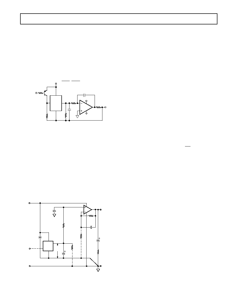
OP179/OP279
≠9≠
REV. F
ON-OFF settling time of the circuit, R2 can be reduced to
50 k
or less. Although the integrator's time constant chosen
here is 1 ms, room exists to trade-off circuit bandwidth and
noise by increasing R3 and decreasing C2. The SHUTDOWN
feature is maintained in the circuit with the simple addition of a
PNP transistor and a 10 k
resistor. One caveat with this ap-
proach should be mentioned: although rail-to-rail output ampli-
fiers work best in the application, these operational amplifiers
require a finite amount (mV) of headroom when required to
provide any load current. The choice for the circuit's negative
supply should take this issue into account.
R4
10
1/2
OP279
+5V
≠10V
R3
1k
C2
1 F
C1
1 F
R2
100k
U1
REF195
GND
R5
10k
R1
10k
2N3904
4
6
2
3
SHUTDOWN
TTL/CMOS
+5V
≠V
REF
U1
REF192
REF193
REF196
REF194
V
OUT
(V)
2.5
3.0
3.3
4.5
Figure 29. A Negative Precision Voltage Reference That
Uses No Precision Resistors Exhibits High Output Current
Drive
A High Output Current, Buffered Reference/Regulator
Many applications require stable voltage outputs relatively close
in potential to an unregulated input source. This "low dropout"
type of reference/regulator is readily implemented with a rail-to-
rail output op amp, and is particularly useful when using a
higher current device such as the OP179/OP279. A typical
example is the 3.3 V or 4.5 V reference voltage developed from
a 5 V system source. Generating these voltages requires a three-
terminal reference, such as the REF196 (3.3 V) or the REF194
(4.5 V), both of which feature low power, with sourcing outputs
of 30 mA or less. Figure 30 shows how such a reference can be
outfitted with an OP179/OP279 buffer for higher currents and/
or voltage levels, plus sink and source load capability.
C2
0.1 F
R2
10k
1%
U2
1/2 OP279
V
OUT1
=
3.3V @ 30mA
R5
1
C5
10 F/25V
TANTALUM
R1
10k
1%
C1
0.1 F
+V
S
+5V
V
OUT2
=
3.3V
C4
1 F
6
2
3
4
V
OUT
COMMON
C3
0.1 F
V
C
ON/OFF
CONTROL
INPUT CMOS HI
(OR OPEN) = ON
LO = OFF
V
S
COMMON
R3
(SEE TEXT)
R4
3.3k
U1
REF196
Figure 30. A High Output Current Reference/Regulator
The low dropout performance of this circuit is provided by stage
U2, one-half of an OP179/OP279 connected as a follower/buffer
for the basic reference voltage produced by U1. The low voltage
saturation characteristic of the OP179/OP279 allows up to 30 mA
of load current in the illustrated use, as a 5 V to 3.3 V converter
with high dc accuracy. In fact, the dc output voltage change for
a 30 mA load current delta measures less than 1 mV. This
corresponds to an equivalent output impedance of < 0.03
. In
this application, the stable 3.3 V from U1 is applied to U2
through a noise filter, R1-C1. U2 replicates the U1 voltage
within a few mV, but at a higher current output at V
OUT1
, with
the ability to both sink and source output current(s)--unlike
most IC references. R2 and C2 in the feedback path of U2
provide bias compensation for lowest dc error and additional
noise filtering.
Transient performance of the reference/regulator for a 10 mA
step change in load current is also quite good and is determined
largely by the R5-C5 output network. With values as shown, the
transient is about 10 mV peak and settles to within 2 mV in
8
µ
s, for either polarity. Although room exists for optimizing the
transient response, any changes to the R5-C5 network should be
verified by experiment to preclude the possibility of excessive
ringing with some capacitor types.
To scale V
OUT2
to another (higher) output level, the optional
resistor R3 (shown dotted) is added, causing the new V
OUT1
to
become:
V
OUT 1
=
V
OUT 2
◊
1
+
R2
R3
As an example, for a V
OUT1
= 4.5 V, and V
OUT2
= 2.5 V from a
REF192, the gain required of U2 is 1.8 times, so R2 and R3
would be chosen for a ratio of 0.8:1, or 18 k
:22.5 k
. Note
that for the lowest V
OUT1
dc error, the parallel combination of
R2 and R3 should be maintained equal to R1 (as here), and the
R2-R3 resistors should be stable, close tolerance metal film
types.
The circuit can be used as shown as either a 5 V to 3.3 V refer-
ence/regulator, or it can be used with ON/OFF control. By
driving Pin 3 of U1 with a logic control signal as noted, the
output is switched ON/OFF. Note that when ON/OFF control
is used, resistor R4 should be used with U1 to speed ON-OFF
switching.
Direct Access Arrangement for Telephone Line Interface
Figure 31 illustrates a +5 V only transmit/receive telephone line
interface for 110
transmission systems. It allows full duplex
transmission of signals on a transformer coupled 110
line in a
differential manner. Amplifier A1 provides gain that can be
adjusted to meet the modem output drive requirements. Both
A1 and A2 are configured to apply the largest possible signal on a
single supply to the transformer. Because of the OP179/
OP279's high output current drive and low dropout voltage, the
largest signal available on a single +5 V supply is approximately
4.5 V p-p into a 110
transmission system. Amplifier A3 is
configured as a difference amplifier to extract the receive signal
from the transmission line for amplification by A4. A4's gain
can be adjusted in the same manner as A1's to meet the modem's
input signal requirements. Standard resistor values permit the
use of SIP (Single In-line Package) format resistor arrays. Couple
this with the OP179/OP279's 8-lead SOIC footprint and this
circuit offers a compact, cost-sensitive solution.

OP179/OP279
≠10≠
REV. F
6.2V
6.2V
TRANSMIT
TXA
RECEIVE
RXA
C1
0.1 F
R1
10k
R2
9.09k
2k
P1
TX GAIN
ADJUST
A1
A2
A3
A4
A1, A2 = 1/2 OP279
A3, A4 = 1/2 OP279
R3
55
R4
55
1:1
T1
TO TELEPHONE
LINE
1
2
3
7
6
5
2
3
1
6
5
7
10 F
R7
10k
R8
10k
R5
10k
R6
10k
R9
10k
R14
9.09k
R10
10k
R11
10k
R12
10k
R13
10k
C2
0.1 F
P2
RX GAIN
ADJUST
2k
Z
O
110
+5V DC
Figure 31. A Single Supply Direct Access Arrangement for
Modems
A Single Supply, Remote Strain Gage Signal Conditioner
The circuit in Figure 32 illustrates a way by which the OP179/
OP279 can be used in a +12 V single supply, 350
strain gage
signal conditioning circuit. In this circuit, the OP179/OP279
serves two functions: (1) By servoing the output of the REF43's
+2.5 V output across R1, it provides a 20 mA drive to the 350
strain gage. In this way, small changes in the strain gage pro-
duce large differential output voltages across the AMP04's in-
puts. (2) To maximize the circuit's dynamic range, the other
half of the OP179/OP279 is configured as a supply-splitter
connected to the AMP04's REF terminal. Thus, tension or
compression in the application can be measured by the circuit.
REF43
AMP04
0.1 F
2
6
4
+2.5V
3
1
8
4
2
A1
7
1
8
6
3
2
4
C
X
C2
0.1 F
R4
1k
+12V
5
V
O
80mV/
V
O
COMMON
R1
124
0.1%, LOW TCR
100-ft TWISTED PAIR
BELDEN TYPE 9502
S+
S≠
350
STRAIN GAGE
F≠
F+
A2
+12V
R2
10k
R3
10k
C1
10 F
7
6
5
+6V
A1, A2 = 1/2 OP279
+12V
20mA DRIVE
Figure 32. A Single Supply, Remote Strain Gage Signal
Conditioner
The AMP04 is configured for a gain of 100, producing a circuit
sensitivity of 80 mV/
. Capacitor C2 is used across the AMP04's
Pins 8 and 6 to provide a 16-Hz noise filter. If additional noise
filtering is required, an optional capacitor, C
X
, can be used
across the AMP04's input to provide differential-mode noise
rejection.
A Single Supply, Balanced Line Driver
The circuit in Figure 33 is a unique line driver circuit topology
used in professional audio applications and has been modified
for automotive audio applications. On a single +12 V supply,
the line driver exhibits less than 0.02% distortion into a 600
load across the entire audio band (not shown). For loads greater
than 600
, distortion performance improves to where the cir-
cuit exhibits less than 0.002%. The design is a transformerless,
balanced transmission system where output common-mode
rejection of noise is of paramount importance. Like the trans-
former-based system, either output can be shorted to ground for
unbalanced line driver applications without changing the circuit
gain of 1. Other circuit gains can be set according to the equa-
tion in the diagram. This allows the design to be easily config-
ured for noninverting, inverting, or differential operation.
R
L
600
C1
22 F
A2
7
6
5
3
1
2
A1
+12V
R1
10k
R2
10k
R11
10k
R7
10k
6
7
5
A1
+12V
+12V
R8
100k
R9
100k
C2
1 F
R12
10k
R14
50
A2
1
2
3
R3
10k
R6
10k
R13
10k
C3
47 F
V
O1
V
O2
C4
47 F
A1, A2 = 1/2 OP279
GAIN = R3
R2
SET: R7, R10, R11 = R2
SET: R6, R12, R13 = R3
V
IN
R5
50
Figure 33. A Single Supply, Balanced Line Driver for
Automotive Applications
OP179/OP279
≠11≠
REV. F
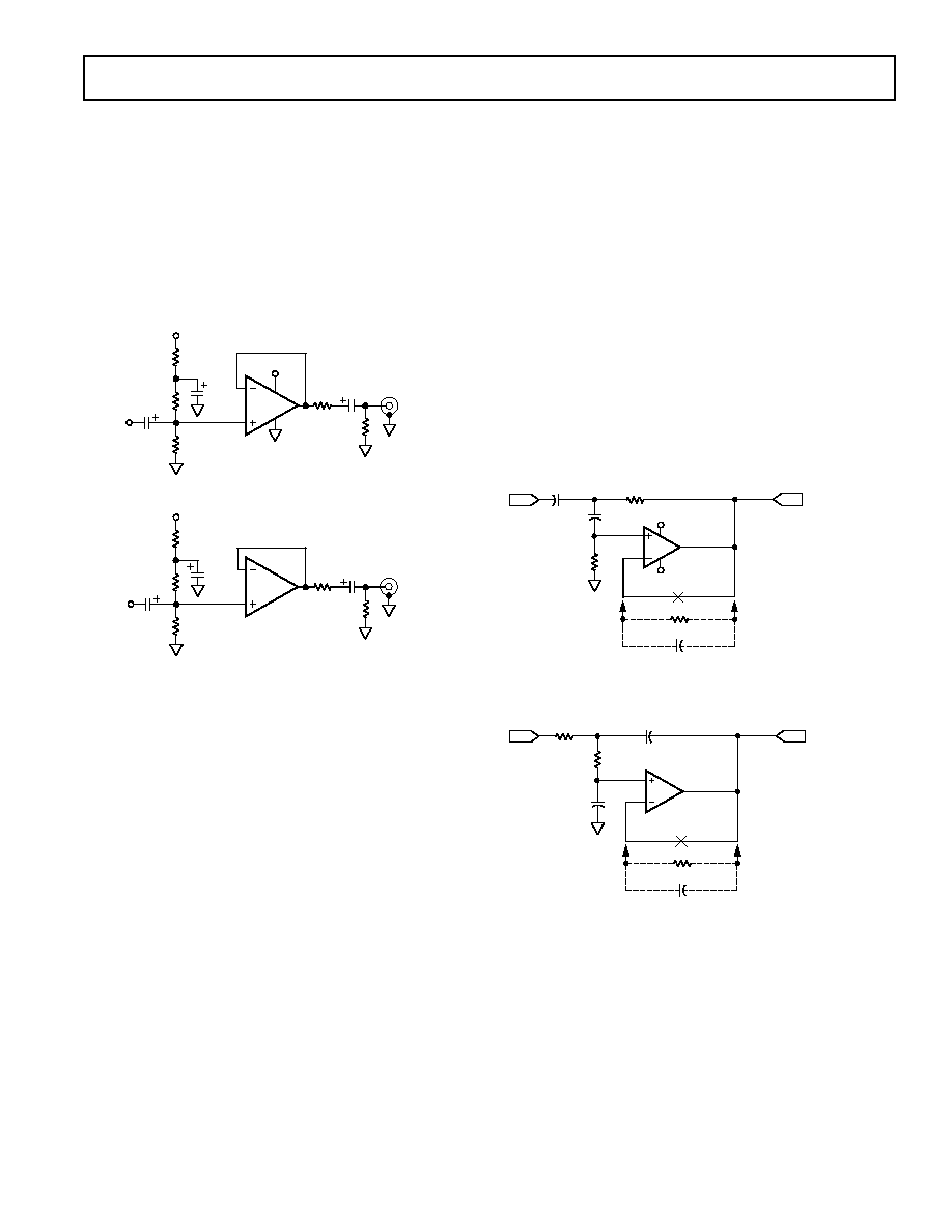
UNITY-GAIN, SALLEN-KEY (VCVS) FILTERS
High Pass Configurations
In Figure 35a is the HP form of a unity-gain 2-pole SK filter
using an OP179/OP279 section. For this filter and its LP coun-
terpart, the gain in the passband is inherently unity, and the
signal phase is noninverting due to the follower hookup. For
simplicity and practicality, capacitors C1-C2
are set equal, and
resistors R2-R1
are adjusted to a ratio "N," which provides the
filter damping "
" as per the design expressions. A HP design
is begun with selection of standard capacitor values for C1 and
C2 and a calculation of N; then R1 and R2 are calculated as per
the figure expressions.
In these examples,
(or 1/Q) is set equal to
2, providing a
Butterworth (maximally flat) response characteristic. The filter
corner frequency is normalized to 1 kHz, with resistor values
shown in both rounded and (exact) form. Various other 2-pole
response shapes are also possible with appropriate selection of
. For a given response type (
), frequency can be easily scaled,
using proportional R or C values.
+V
S
≠V
S
U1A
OP279
1
3
2
4
8
IN
R2
22k
(22.508k )
R1
11k
(11.254k )
C2
0.01 F
R = R2
0.1 F
Z
f
(HIGH PASS)
C1
0.01 F
GIVEN: ALPHA, F
SET C1 = C2 = C
ALPHA = 2/(N^0.5) = 1/Q
N = 4/(ALPHA)^2 = R2/R1
R1 = 1/(2*PI*F*C* (N^0.5))
R2 = N*R1
1kHz BW SHOWN
OUT
7
5
6
R = R1+R2
Z
f
(LOW PASS)
GIVEN: ALPHA, F
SET R1 = R2 = R
ALPHA = 2/(M^0.5) = 1/Q
N = 4/(ALPHA)^2 = C2/C1
PICK C1
C1 = M*C1
R = 1/(2*P1*F*C1* (M^0.5))
1kHz BW SHOWN
IN
R2
11k
(11.254k )
C2
0.01 F
0.1 F
C1
0.02 F
OUT
U1B
OP279
R1
11k
(11.254k )
a. High Pass
b. Low Pass
Figure 35. 2-Pole Unity-Gain Sallen Key HP/LP Filters
Low Pass Configurations
In the LP SK arrangement of Figure 35b, R and C elements are
interchanged, and the resistors are made equal. Here the C2/C1
ratio "M" is used to set the filter
, as noted. This design is begun
with the choice of a standard capacitor value for C1 and a calcu-
lation of M, which forces a value of "M
◊
C1" for C2. Then, the
value "R" for R1 and R2 is calculated as per the expression.
For highest performance, the passive components used for tun-
ing active filters deserve attention. Resistors should be 1%, low
TC, metal film types of the RN55 or RN60 style, or similar.
A Single Supply Headphone Amplifier
Because of its high speed and large output drive, the OP179/
OP279 makes for an excellent headphone driver, as illustrated
in Figure 34. Its low supply operation and rail-to-rail inputs
and outputs give a maximum signal swing on a single +5 V
supply. To ensure maximum signal swing available to drive the
headphone, the amplifier inputs are biased to V+/2, which is in
this case 2.5 V. The 100 k
resistor to the positive supply is
equally split into two 50 k
with their common point bypassed
by 10
µ
F to prevent power supply noise from contaminating the
audio signal.
16
50k
220 F
LEFT
HEADPHONE
10 F
50k
50k
100k
10 F
LEFT
INPUT
+V + 5V
1/2
OP279
16
50k
220 F
RIGHT
HEADPHONE
10 F
50k
50k
100k
10 F
RIGHT
INPUT
+V
+V + 5V
1/2
OP279
Figure 34. A Single Supply, Stereo Headphone Driver
The audio signal is then ac-coupled to each input through a
10
µ
F capacitor. A large value is needed to ensure that the
20 Hz audio information is not blocked. If the input already has
the proper dc bias, the ac coupling and biasing resistors are not
required. A 220
µ
F capacitor is used at the output to couple the
amplifier to the headphone. This value is much larger than that
used for the input because of the low impedance of the head-
phones, which can range from 32
to 600
. An additional
16
resistor is used in series with the output capacitor to pro-
tect the op amp's output stage by limiting capacitor discharge
current. When driving a 48
load, the circuit exhibits less than
0.02% THD+N at low output drive levels (not shown). The
OP179/OP279's high current output stage can drive this heavy
load to 4 V p-p and maintain less than 1% THD+N.
Active Filters
Several active filter topologies are useful with the OP179/OP279.
Among these are two popular architectures, the familiar Sallen-
Key (SK) voltage controlled voltage source (VCVS) and the
multiple feedback (MFB) topologies. These filter types can be
arranged for high pass (HP), low pass (LP), and bandpass (BP)
filters. The SK filter type uses the op amp as a fixed gain voltage
follower at unity or a higher gain, while the MFB structure uses
it as an inverting stage. Discussed here are simplified, 2-pole
forms of these filters, highly useful as system building blocks.

OP179/OP279
≠12≠
REV. F
reactive, and limits overall practicality of this filter. The dire
effect of C1 loading can be tempered somewhat by using a small
series input resistance of about 100
, but can still be an issue.
7
6
5
0.1 F
GIVEN:
ALPHA, F AND H (PASSBAND GAIN)
ALPHA = 1/Q
PICK A STD C1 VALUE, THEN:
C3 = C1, C2 = C1/H
R1 = ALPHA / ((2*PI*F*C1)*(2+(1/H)))
R2 = (H*(2+(1/H))) / (ALPHA*(2*PI*F*C1))
1kHz BW EXAMPLE SHOWN
(NOTE: SEE TEXT ON C1 LOADING
CONSIDERATIONS)
IN
R1
7.5k
OUT
U1B
OP279
R2
33.6k
C3
0.01 F
C2
0.01 F
C1
0.01 F
Z
b
R = R2
Figure 36. Two-Pole, High Pass Multiple Feedback Filters
In this example, the filter gain is set to unity, the corner fre-
quency is 1 kHz, and the response is a Butterworth type. For
applications where dc output offset is critical, bias current com-
pensation can be used for the amplifier. This is provided by
network Z
b
, where R is equal to R2, and the capacitor provides
a noise bypass.
Low Pass Configurations
Figure 37 is a LP MFB 2-pole filter using an OP179/OP279
section. For this filter, the gain in the pass band is user config-
urable over a wide range, and the pass band signal phase is
inverting. Given the design parameters for
, F, and H, a sim-
plified design process is begun by picking a standard value for
C2. Then C1
and resistors R1-R3
are selected as per the rela-
tionships noted. Optional dc bias current compensation is pro-
vided by Z
b
, where R is equal to the value of R3 plus the parallel
equivalent value of R1
and R2.
7
5
6
(R1
R2)+R3
GIVEN:
ALPHA, F AND H (PASSBAND GAIN)
ALPHA = 1/Q
PICK A STD C2 VALUE, THEN:
C1 = C2 ∑ (4 ∑ (H +1))/ALPHA^2
R1 = ALPHA/(4 ∑ H ∑ PI ∑ F ∑ C2)
R2 = H ∑ R1
R3 = ALPHA/(4 ∑ (H + 1) ∑ PI ∑ F ∑ C2)
1kHz BW EXAMPLE SHOWN
(NOTE: SEE TEXT ON C1 LOADING
CONSIDERATIONS)
IN
OUT
U1B
OP279
R1
11.3k
R2
11.3k
R3
5.62k
C2
0.01 F
0.1 F
Z
b
C1
0.04 F
Figure 37. Two-Pole, Low-Pass Multiple Feedback Filters
Gain of this filter, H, is set here by resistors R2 and R1 (as in a
standard op amp inverter), and can be just as precise as these
resistors allow at low frequencies. Because of this flexible and
accurate gain characteristic, plus a low range of component
value spread, this filter is perhaps the most practical of all the
MFB types. Capacitor ratios are best satisfied by paralleling
two or more common types, as in the example, which is a 1 kHz
unity gain Butterworth filter.
Capacitors should be 1% or 2% film types preferably, such as
polypropylene or polystyrene, or NPO (COG) ceramic for
smaller values. Somewhat lesser performance is available with
the use polyester capacitors.
Parasitic Effects in Sallen-Key Implementations
In designing these circuits, moderately low (10 k
or less) val-
ues for R1-R2 can be used to minimize the effects of Johnson
noise when critical, with of course practical tradeoffs of capaci-
tor size and expense. DC errors will result for larger values of
resistance, unless bias current compensation is used. To add
bias compensation in the HP filter of Figure 35a, a feedback
compensation resistor with a value equal to R2 is used, shown
optionally as Z
f
. This will minimize bias induced offset, reduc-
ing it to the product of the OP179/OP279's I
OS
and R2. Similar
compensation is applied to the LP filter, using a Z
f
resistance of
R1 + R2. Using dc compensation and relatively low filter val-
ues, filter output dc errors using the OP179/OP279 will be
dominated by V
OS
, which is limited to 4 mV or less. A caveat
here is that the additional resistors increase noise substantially--
for example, an unbypassed 10 k
resistor generates
12 nV/
Hz of noise. However, the resistance can be ac-bypassed to
eliminate noise with a simple shunt capacitor, such as 0.1
µ
F.
Sallen-Key Implementations in Single Supply Applications
The hookups shown illustrate a classical dual supply op amp
application, which for the OP179/OP279 would use supplies up
to
±
5 V. However, these filters can also use the op amp in a
single-supply mode, with little if any alteration to the filter itself.
To operate single-supply, the OP179/OP279 is powered from
+5 V at Pin 8 with Pin 4 grounded. The input dc bias for the
op amp must be supplied from a dc source equal to 1/2 supply,
or 2.5 V in this case.
For the HP section, dc bias is applied to the common end of R2.
R2 is simply returned to an ac ground that is a well-bypassed
2:1 divider across the 5 V source. This can be as simple as a
pair of 100 k
resistors with a 10
µ
F bypass cap. The output
from the stage is then ac coupled, using an appropriate coupling
cap from U1A to the next stage. For the LP section dc bias is
applied to the input end of R1, in common with the input sig-
nal. This dc can be taken from an unbypassed dual 100 k
divider across the supply, with the input signal ac coupled to the
divider and R1.
Multiple Feedback Filters
MFB filters, like their SK relatives, can be used as building
blocks as well. They feature LP and HP operation as well, but
can also be used in a bandpass BP mode. They have the prop-
erty of inverting operation in the pass band, since they are based
on an inverting amplifier structure. Another useful asset is their
ability to be easily configured for gain.
High Pass Configurations
Figure 36 shows an HP MFB 2-pole filter using an OP179/
OP279 section. For this filter, the gain in the passband is user
configurable, and the signal phase is inverting. The circuit uses
one more tuning component than the SK types. For simplicity,
capacitors C1 and C3
are set to equal standard values, and
resistors R1-R2
are selected as per the relationships noted. Gain
of this filter, H, is set by capacitors C1 and C2, and this factor
limits both gain selectability and precision. Also, input capaci-
tance C1 makes the load seen by the driving stage highly

OP179/OP279
≠13≠
REV. F
V
IN
3
2
1
U1A
OP279
+V
S
4
≠V
S
R1
31.6k
C1
0.01 F
C2
0.01 F
R2
31.6k
R5
31.6k
R6
31.6k
R4
49.9
HI
LO
500Hz AND UP
DC ≠ 500Hz
6
5
7
C3
0.01 F
U1B
OP279
C4
0.02 F
R7
15.8k
R3
49.9
0.1 F
0.1 F
100 F/25V
100 F/25V
+V
S
≠V
S
TO U1
+5V
≠5V
COM
Figure 39. Two-Way Active Crossover Networks
In the filter sections, component values have been selected for
good balance between reasonable physical/electrical size, and
lowest noise and distortion. DC offset errors can be minimized
by using dc compensation in the feedback and bias paths, ac
bypassed with capacitors for low noise. Also, since the network
input is reactive, it should driven from a directly coupled low
impedance source at V
IN
.
Figure 40 shows this filter architecture adapted for single supply
operation from a 5 V dc source, along the lines discussed
previously.
V
IN
3
2
1
U1A
OP279
+V
S
4
R1
31.6k
C1
0.01 F
C2
0.01 F
R2
31.6k
R5
31.6k
R6
31.6k
R4
49.9
HI
LO
500Hz
AND UP
DC ≠
500Hz
6
5
7
C3
0.01 F
U1B
OP279
C4
0.02 F
R7
15.8k
R3
49.9
10 F
10 F
100k
+V
S
10 F
100k
100k
C
IN
10 F
R
IN
100k
0.1 F
100 F/25V
+V
S
TO U1
+5V
COM
+
100k
+
Figure 40. A Single Supply, Two-Way Active Crossover
Bandpass Configurations
The MFB bandpass filter using an OP179/OP279 section is
shown in Figure 38. This filter provides reasonably stable me-
dium Q designs for frequencies of up to a few kHz. For best
predictability and stability, operation should be restricted to
applications where the OP179/OP279 has an open-loop gain in
excess of 2Q
2
at the filter center frequency.
7
6
5
R = R3
0.1 F
GIVEN:
Q, F, AND A
O
(PASSBAND GAIN)
ALPHA = 1/Q, H = A
O
/Q
PICK A STD C1 VALUE, THEN:
C2 = C1
R1 = 1/(H*(2*PI*F*C1))
R2 = 1/(((2*Q) ≠H)*(2*PI*F*C1))
R3 = Q/(PI*F*C1)
EXAMPLE: 60Hz, Q = 10,
A
O
= 10 (OR 1)
A
O
= 1 FOR '( )' VALUES
IN
R2
1.4k
(1.33k )
OUT
U1B
OP279
R3
530k
C2
0.1 F
C1
0.1 F
Z
b
R1
26.4k
(264k )
Figure 38. Two-Pole, Bandpass Multiple Feedback Filters
Given the bandpass design parameters for Q, F, and pass band
gain A
O
, the design process is begun by picking a standard value
for C1. Then C2
and resistors R1-R3
are selected as per the
relationships noted. This filter is subject to a wide range of
component values by nature. Practical designs should attempt
to restrict resistances to a 1 k
to 1 M
range, with capacitor
values of 1
µ
F or less. When needed, dc bias current compensa-
tion is provided by Z
b
, where R is equal to R3.
Two-Way Loudspeaker Crossover Networks
Active filters are useful in loudspeaker crossover networks for
reasons of small size, relative freedom from parasitic effects, and
the ease of controlling low/high channel drive, plus the con-
trolled driver damping provided by a dedicated amplifier. Both
Sallen-Key (SK) VCVS and multiple-feedback (MFB) filter
architectures are useful in implementing active crossover net-
works (see Reference 4), and the circuit shown in Figure 39 is
a two-way active crossover which combines the advantages of
both filter topologies. This active crossover exhibits less than
0.01% THD+N at output levels of 1 V rms using general pur-
pose unity gain HP/LP stages. In this two-way example, the LO
signal is a dc-500 Hz LP woofer output, and the HI signal is the
HP (> 500 Hz) tweeter output. U1B forms a MFB LP section
at 500 Hz, while U1A provides a SK HP section, covering fre-
quencies
500 Hz.
This crossover network is a Linkwitz-Riley type
(see Reference
5), with a damping factor or
of 2 (also referred to as
"Butterworth squared"). A hallmark of the Linkwitz-Riley type
of filter is the fact that the summed magnitude response is flat
across the pass band. A necessary condition for this to happen
is the relative signal polarity of the HI output must be inverted
with respect to the LOW outputs. If only SK filter sections
were used, this requires that the connections to one speaker be
reversed on installation. Alternately, with one inverting stage
used in the LO channel, this accomplishes the same effect. In
the circuit as shown, stage U1B is the MFB LP filter which
provides the necessary polarity inversion. Like the SK sections,
it is configured for unity gain and an
of 2. The cutoff frequency
is 500 Hz, which complements the SK HP section of U4.
OP179/OP279
≠14≠
REV. F
References on Active Filters and Active Crossover Networks
1. Sallen, R.P.; Key, E.L., "A Practical Method of Designing
RC Active Filters," IRE Transactions on Circuit Theory, vol.
CT-2, March 1955.
2. Huelsman, L.P.; Allen, P.E., Introduction to the Theory and
Design of Active Filters, McGraw-Hill, 1980.
3. Zumbahlen, H., "Chapter 6: Passive and Active Analog
Filtering," within 1992 Analog Devices Amplifier Applications
Guide.
4. Zumbahlen, H., "Speaker Crossovers," within Chapter 8 of
1993 Analog Devices System Applications Guide.
5. Linkwitz, S., "Active Crossover Networks for Noncoincident
Drivers," JAES, Vol. 24, #1, Jan/Feb 1976.
The crossover example frequency of 500 Hz can be shifted
lower or higher by frequency scaling of either resistors or capaci-
tors. In configuring the circuit for other frequencies, comple-
mentary LP/HP action must be maintained between sections,
and component values within the sections must be in the same
ratio. Table II provides a design aid to adaptation, with sug-
gested standard component values for other frequencies.
Table II. RC Component Selection for Various Crossover
Frequencies
R1/C1 (U1A)*
Crossover Frequency (Hz)
R5/C3 (U1B)**
100
160 k
/0.01
µ
F
200
80.6 k
/0.01
µ
F
319
49.9 k
/0.01
µ
F
500
31.6 k
/0.01
µ
F
1 k
16 k
/0.01
µ
F
2 k
8.06 k
/0.01
µ
F
5 k
3.16 k
/0.01
µ
F
10 k
1.6 k
/0.01
µ
F
Table notes (applicable for
= 2).
* For SK stage U1A: R1 = R2, and C1 = C2, etc.
** For MFB stage U1B: R6 = R5, R7 = R5/2, and C4 = 2C3.

OP179/OP279
≠15≠
REV. F
R10
16
98
10
C3
15
16
15.915E-12
*
* ZERO AT 1.5 MHz
*
E1
14
98
(9,39) 1E6
R5
14
18
1E6
R6
18
98
1
C4
14
18
106.103E-15
*
* BIAS CURRENT-VS-COMMON-MODE VOLTAGE
*
EP
97
0
(99,0) 1
EN
51
0
(50,0) 1
V3
20
21
1.6
V4
22
23
2.8
R12
97
20
530
R13
23
51
1E3
D13
15
21
DX
D14
22
15
DX
FIB
98
24
POLY(2) V3 V4 0 ≠1 1
RIB
24
98
10E3
E3
97
25
POLY(1) (99,39) ≠1.63 1
E4
26
51
POLY(1) (39,50) ≠2.73 1
D15
24
25
DX
D16
26
24
DX
*
* POLE AT 6 MHz
*
G6
98
40
(18,39)
1E
6
R20
40
98
1E6
C10
40
98
26.526E-15
*
* OUTPUT STAGE
*
RS1
99
39
6.0345E3
RS2
39
50
6.0345E3
RO1
99
45
40
RO2
45
50
40
G7
45
99
(99,40) 25E-3
G8
50
45
(40,50) 25E-3
G9
98
60
(45,40) 25E-3
D9
60
61
DX
D10
62
60
DX
V7
61
98
DC
0
V8
98
62
DC 0
FSY
99
50
POLY(2) V7 V8 1.711E-3
1
1
D11
41
45
DZ
D12
45
42
DZ
V5
40
41
1.54
V6
42
40
1.54
.MODEL
DX
D()
.MODEL
DZ
D(IS=1E-6)
.MODEL
QN NPN(BF=300)
.ENDS
OP179/OP279 Spice Macro Model
* OP179/OP279 SPICE Macro-model Rev. A, 5/94
* ARG / ADI
*
* Copyright 1994 by Analog Devices
*
* Refer to "README.DOC" file for License Statement. Use of
* this model indicates your acceptance of the terms and pro-
* visions in the License Statement.
*
* Node assignments
*
noninverting input
*
|
inverting input
*
|
|
positive supply
*
|
|
|
negative supply
*
|
|
|
|
output
*
|
|
|
|
|
.SUBCKT OP179/OP279 3
2
99 50 45
*
* INPUT STAGE AND POLE AT 6 MHz
*
I1
1
50
60.2E-6
Q1
5
2
7 QN
Q2
6
4
8 QN
D1
4
2
DX
D2
2
4
DX
R1
1
7
1.628E3
R2
1
8
1.628E3
R3
5
99
2.487E3
R4
6
99
2.487E3
C1
5
6
5.333E-12
EOS
4
3
POLY(1) (16,39) 0.25E-3 50.118
IOS
2
3
5E-9
GB1
2
98
(24,98) 100E-9
GB2
4
98
(24,98) 100E-9
CIN
2
3
1E-12
*
* GAIN STAGE AND DOMINANT POLE AT 16 Hz
*
EREF
98
0
(39,0) 1
G1
98
9
(5,6) 402.124E-6
R7
9
98
497.359E6
C2
9
98
20E-12
V1
99
10
0.58
V2
11
50
0.47
D5
9
10
DX
D6
11
9
DX
*
* COMMON-MODE STAGE WITH ZERO AT 10 kHz
*
ECM
15
98
POLY(2) (3,39) (2,39) 0 0.5 0.5
R9
15
16
1E6
OP179/OP279
≠16≠
REV. F
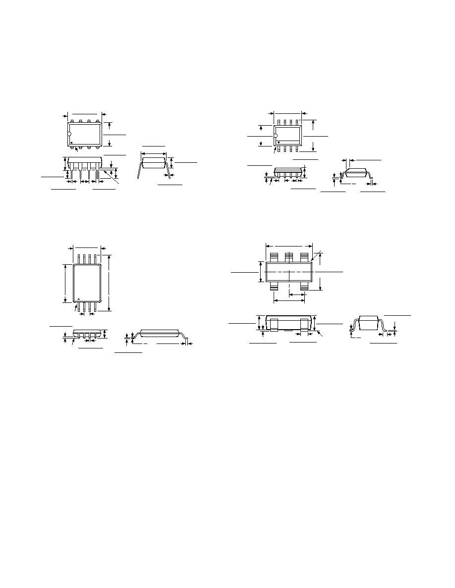
OUTLINE DIMENSIONS
Dimensions shown in inches and (mm).
C3497a≠0≠10/99
PRINTED IN U.S.A.
8-Lead Plastic DIP
(N-8)
8
1
4
5
0.430 (10.92)
0.348 (8.84)
0.280 (7.11)
0.240 (6.10)
PIN 1
SEATING
PLANE
0.022 (0.558)
0.014 (0.356)
0.060 (1.52)
0.015 (0.38)
0.210 (5.33)
MAX
0.130
(3.30)
MIN
0.070 (1.77)
0.045 (1.15)
0.100
(2.54)
BSC
0.160 (4.06)
0.115 (2.93)
0.325 (8.25)
0.300 (7.62)
0.015 (0.381)
0.008 (0.204)
0.195 (4.95)
0.115 (2.93)
8-Lead TSSOP
(RU-8)
8
5
4
1
0.122 (3.10)
0.114 (2.90)
0.256 (6.50)
0.246 (6.25)
0.177 (4.50)
0.169 (4.30)
PIN 1
0.0256 (0.65)
BSC
SEATING
PLANE
0.006 (0.15)
0.002 (0.05)
0.0118 (0.30)
0.0075 (0.19)
0.0433
(1.10)
MAX
0.0079 (0.20)
0.0035 (0.090)
0.028 (0.70)
0.020 (0.50)
8
0
8-Lead Narrow-Body SO
(SO-8)
0.1968 (5.00)
0.1890 (4.80)
8
5
4
1
0.2440 (6.20)
0.2284 (5.80)
PIN 1
0.1574 (4.00)
0.1497 (3.80)
0.0688 (1.75)
0.0532 (1.35)
SEATING
PLANE
0.0098 (0.25)
0.0040 (0.10)
0.0192 (0.49)
0.0138 (0.35)
0.0500
(1.27)
BSC
0.0098 (0.25)
0.0075 (0.19)
0.0500 (1.27)
0.0160 (0.41)
8∞
0∞
0.0196 (0.50)
0.0099 (0.25)
x 45∞
5-Lead SOT-23
(RT-5)
0.0079 (0.200)
0.0035 (0.090)
0.0236 (0.600)
0.0039 (0.100)
10
0
0.0197 (0.500)
0.0118 (0.300)
0.0590 (0.150)
0.0000 (0.000)
0.0512 (1.300)
0.0354 (0.900)
SEATING
PLANE
0.0571 (1.450)
0.0354 (0.900)
0.1220 (3.100)
0.1063 (2.700)
PIN 1
0.0709 (1.800)
0.0590 (1.500)
0.1181 (3.000)
0.0984 (2.500)
1
3
4
5
0.0748 (1.900)
REF
0.0374 (0.950) REF
2
NOTE:
PACKAGE OUTLINE INCLUSIVE AS SOLDER PLATING.