 | ÐлекÑÑоннÑй компоненÑ: REF01EJ | СкаÑаÑÑ:  PDF PDF  ZIP ZIP |
Äîêóìåíòàöèÿ è îïèñàíèÿ www.docs.chipfind.ru
REV. C
Information furnished by Analog Devices is believed to be accurate and
reliable. However, no responsibility is assumed by Analog Devices for its
use, nor for any infringements of patents or other rights of third parties that
may result from its use. No license is granted by implication or otherwise
under any patent or patent rights of Analog Devices.
a
REF01
One Technology Way, P.O. Box 9106, Norwood, MA 02062-9106, U.S.A.
Tel: 781/329-4700
www.analog.com
Fax: 781/326-8703 © Analog Devices, Inc., 2002
10 V Precision
Voltage Reference
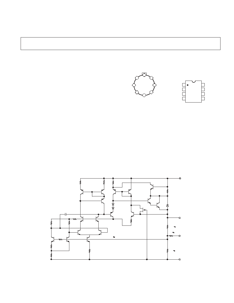
SIMPLIFIED SCHEMATIC
C1
R3
R6
R4
R5
R1
Q1
R2
R10
OUTPUT
GROUND
R12 16.7k
TRIM
Q19
R15
INPUT
Q15
Q18
Q16
Q13
Q21
Q17
R13
Q20
Q4
Q3
Q5
Q6
Q9
Q7
Q14
Q12
Q11
Q8
R8
R7
R14
Q10
Q2
R11 2k
R9 50k
4
5
6
1.23V
2
FEATURES
10 V Output, 0.3% Max
Adjustment Range, 3% Min
Excellent Temperature Stability, 8.5 ppm/ C Max
Low Noise, 30 V p-p Max
Low Supply Current, 1.4 mA Max
Wide Input Voltage Range, 12 V to 40 V
High Load Driving Capability, 20 mA
No External Components
Short Circuit Proof
GENERAL DESCRIPTION
The REF01 precision voltage reference provides a stable 10 V
output that can be adjusted over a 3% range with minimal effect
on temperature stability. Single-supply operation over an input
voltage range of 12 V to 40 V, a low current drain of 1 mA, and
excellent temperature stability are achieved with an improved
band gap design. Low cost, low noise, and low power make the
REF01 an excellent choice whenever a stable voltage reference
is required. Applications include D/A and A/D converters,
portable instrumentation, and digital voltmeters. Full military
temperature range devices with screening to MIL-STD-883
are available. For new designs, please refer to ADR01.
Epoxy MINI-DIP (P-Suffix)
8-Lead Hermetic DIP (Z-Suffix)
8-Lead SO (S-Suffix)
8
7
6
5
1
2
3
4
NC = NO CONNECT*
NC
V
IN
NC
NC
NC
V
OUT
TRIM
GND
TOP VIEW
(Not to Scale)
REF01
TO-99 (J-Suffix)
7
8
1
4
5
6
3
2
NC
V
OUT
TRIM
GROUND
(CASE)
NC
NC
V
IN
NC
NC = NO CONNECT*
PIN CONFIGURATION
*NC = No Connect. Do not connect anything on these pins as some
of them are reserved for factory testing purposes.
REV. C
2
REF01SPECIFICATIONS
ELECTRICAL SPECIFICATIONS
REF01A/E
REF01/H
Parameter
Symbol
Conditions
Min
Typ
Max
Min
Typ
Max
Unit
Output Voltage
V
O
I
L
= 0 mA
9.97
10.00
10.03
9.95
10.00
10.05
V
Output Adjustment Range
V
TRIM
R
P
= 10 k
±
3.0
±
3.3
±
3.0
±
3.3
%
Output Voltage Noise
1
e
n p-p
0.1 Hz to 10 Hz
20
30
20
30
µ
V p-p
Line Regulation
2
V
IN
= 13 V to 33 V
0.006
0.010
0.006
0.010
%/V
Load Regulation
2
I
L
= 0 mA to 10 mA
0.005
0.008
0.006
0.010
%/mA
Turn-On Settling Time
3
t
ON
To
±
0.1% of Final Value
5
5
µ
s
Quiescent Supply Current
I
SY
No Load
1.0
1.4
1.0
1.4
mA
Load Current
I
L
10
21
10
21
mA
Sink Current
4
I
S
0.3
0.5
0.3
0.5
mA
Short Circuit Current
I
SC
V
O
= 0
30
30
mA
ELECTRICAL SPECIFICATIONS
REF01A/E
REF01/H
Parameter
Symbol
Conditions
Min
Typ
Max
Min
Typ
Max
Unit
Output Voltage Change
V
OT
0
°
C T
A
70
°
C
0.02
0.06
0.07
0.17
%
with Temperature
5, 6
55
°
C
T
A
+125
°
C
0.06
0.15
0.18
0.45
%
Output Voltage
TCV
O
3.0
8.5
10.0
25.0
ppm/
°
C
Temperature Coefficient
7
Change in V
O
Temperature
R
P
= 10 k
0.7
0.7
ppm/%
Coefficient with Output
Adjustment
Line Regulation
0
°
C T
A
70
°
C
0.007
0.012
0.007
0.012
(V
IN
= 13 V to 33 V)
2
55
°
C T
A
+125
°
C
0.009
0.015
0.009
0.015
%/V
Load Regulation
0
°
C
T
A
70
°
C
0.006
0.010
0.007
0.012
(I
L
= 0 mA to 8 mA)
2
55
°
C T
A
+125
°
C
0.007
0.012
0.009
0.015
%/mA
ELECTRICAL SPECIFICATIONS
REF01C
Parameter
Symbol
Conditions
Min
Typ
Max
Unit
Output Voltage
V
O
I
L
= 0 mA
9.90
10.00
10.10
V
Output Adjustment Range
V
TRIM
R
P
= 10 k
±
2.7
±
3.3
%
Output Voltage Noise
1
e
n p-p
0.1 Hz to 10 Hz
25
35
µ
V p-p
Line Regulation
2
V
IN
= 13 V to 33 V
0.009
0.015
%/V
Load Regulation
2
I
L
= 0 mA to 8 mA
0.006
0.015
%/mA
Turn-On Settling Time
3
t
ON
To
±
0.1% of Final Value
5
µ
s
Quiescent Supply Current
I
SY
No Load
1.0
1.6
mA
Load Current
I
L
8
21
mA
Sink Current
4
I
S
0.3
0.5
mA
Short Circuit Current
I
SC
V
O
= 0
30
mA
(@ V
IN
= 15 V, T
A
= 25 C, unless otherwise noted.)
(@ V
IN
= 15 V, 55 C T
A
+125 C for REF01A/E, and 0 C T
A
70 C for REF01H and
I
L
= 0 mA, unless otherwise noted.)
(@ V
IN
= 15 V, T
A
= 25 C, unless otherwise noted.)
REV. C
3
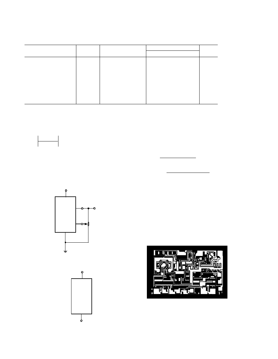
REF01
V
IN
GND
TRIM
V
O
REF01
15V
2
6
5
4
OUTPUT
10k
Figure 1. Output Adjustment
V
IN
GND
REF01
+18V
18V
Figure 2. Burn-In Circuit
The REF01 trim terminal can be used to adjust the output
voltage over a 10 V
±300 mV range. This feature allows the
system designer to trim system errors by setting the reference to
a voltage other than 10 V. Of course, the output can also be set
to exactly 10.000 V or to 10.240 V for binary applications.
Adjustment of the output does not significantly affect the tem-
perature performance of the device. The temperature coefficient
change is approximately 0.7 ppm/
°C for 100 mV of output
adjustment.
2
4
5
6
2. INPUT VOLTAGE (V
IN
)
4. GROUND
5. TRIM
6. OUTPUT VOLTAGE (V
OUT
)
DIE SIZE 0.074 0.048 INCH, 3552 SQUARE MILS
(1.88 1.22 mm, 2.29 SQUARE mm)
Figure 3. Dice Characteristics (125 C Tested Dice Available)
(@ V
IN
= 15 V, 0 C T
A
70 C for REF01CJ, REF01CZ, and
40 C T
A
+85 C for REF01CP and REF01CS, unless otherwise noted.)
ELECTRICAL SPECIFICATIONS
REF01C
Parameter
Symbol
Conditions
Min
Typ
Max
Unit
Output Voltage Change
V
OT
0.14
0.45
%
with Temperature
5, 6
Output Voltage
TCV
O
20
65
ppm/
°C
Temperature Coefficient
7
Change in V
O
Temperature
Coefficient with Output
Adjustment
R
P
= 10 k
0.7
ppm/%
Line Regulation
2
V
IN
= 13 V to 30 V
0.011
0.018
%/V
Load Regulation
2
I
L
= 0 to 5 mA
0.008
0.018
%/mA
TCV
to
C
V
to
C
C
and
TCV
to
C
V
to
C
C
O
OT
O
OT
0
70
0
70
70
55
125
55
125
180
o
o
o
o
o
o
o
o
o
o
+
(
)
=
+
(
)
-
+
(
)
=
-
+
(
)
NOTES
1
Sample tested.
2
Line and load regulation specifications include the effect of self-heating.
3
Guaranteed by design.
4
During sink current test the device meets the output voltage specified.
5
V
OT
is defined as the absolute difference between the maximum output voltage and the minimum
output voltage over the specified temperature range expressed as a percentage of 10 V:
V
V
V
V
OT
MAX
MIN
=
×
10
100
6
V
OT
specification applies trimmed to +10,000 V or untrimmed.
7
TCV
O
is defined as Var divided by the temperature range, i.e.
Specifications are subject to change without notice.
REV. C
REF01
4
WAFER TEST LIMITS
REF01NT
REF01N
REF01GT
REF01G
Parameter
Symbol
Conditions
Limit
Limit
Limit
Limit
Unit
Output Voltage
V
O
I
L
= 0
10.05
10.03
10.10
10.05
V max
9.95
9.97
9.90
9.95
V min
Output Adjustment
Range
V
TRIM
R
P
= 10 k
±
3.0
±
3.0
% min
Line Regulation
V
IN
= 13 V to 33 V
0.015
0.01
0.015
0.01
%/V max
*Electrical tests are performed at wafer probe to the limits shown. Due to variations in assembly methods and normal yield loss, yield after packaging is not guaranteed
for standard product dice. Consult factory to negotiate specifications based on dice lot qualification through sample lot assembly and testing.
(@ V
IN
= 15 V, T
A
= 25 C for REF01N and REF01G devices, T
A
= 125 C for REF01NT and REF01GT devices,
unless otherwise noted.)*
TYPICAL ELECTRICAL CHARACTERISTICS
REF01NT
REF01N
REF01GT
REF01G
Parameter
Symbol
Conditions
Typical
Typical
Typical
Typical
Unit
Load Regulation
I
L
= 0 mA to 10 mA
I
L
= 0 mA to 8 mA,
NT, GT @ 125
°
C
0.007
0.005
0.009
0.006
%/mA
Output Voltage
Noise
e
n p-p
0.1 Hz to 10 Hz
20
20
20
20
µ
V p-p
Turn-On Settling
To
±
0.1% of Final
Time
t
ON
Value NT, GT @
125
°
C
7.5
5.0
7.5
5.0
µ
s
Quiescent Current
I
SY
No Load, NT,
GT @ 125
°
C
1.4
1.0
1.4
1.0
mA
Load Current
I
L
21
21
21
21
mA
Sink Current
I
S
0.5
0.5
0.5
0.5
mA
Short Circuit
Current
I
SC
V
O
= 0
30
30
30
30
mA
Output Voltage
Temperature
Coefficient
TCV
O
10
10
10
10
ppm/
°
C
*For 25
°
C specifications of REF01NT and REF01GT, see REF01N and REF01G, respectively.
(@ V
IN
= 15 V, T
A
= 25 C, unless otherwise noted.)*

REV. C
5
REF01
CAUTION
ESD (electrostatic discharge) sensitive device. Electrostatic charges as high as 4000 V readily
accumulate on the human body and test equipment and can discharge without detection. Although
the REF01 features proprietary ESD protection circuitry, permanent damage may occur on devices
subjected to high energy electrostatic discharges. Therefore, proper ESD precautions are
recommended to avoid performance degradation or loss of functionality.
WARNING!
ESD SENSITIVE DEVICE
ABSOLUTE MAXIMUM RATINGS
*
Input Voltage . . . . . . . . . . . . . . . . . . . . . . . . . . . . . . . . . . 40 V
Output Short Circuit Duration
(to Ground or V
IN
) . . . . . . . . . . . . . . . . . . . . . . . . Indefinite
Storage Temperature Range
J, RC, and Z Packages . . . . . . . . . . . . . . . 65
°
C to +150
°
C
P Package . . . . . . . . . . . . . . . . . . . . . . . . . 65
°
C to +125
°
C
Operating Temperature Range
REF01A . . . . . . . . . . . . . . . . . . . . . . . . . . 55
°
C to +125
°
C
REF01CJ . . . . . . . . . . . . . . . . . . . . . . . . . . . . . 0
°
C to 70
°
C
REF01CP, REF01CS, REF01E,
REF01H . . . . . . . . . . . . . . . . . . . . . . . . . 40
°
C to +85
°
C
Junction Temperature (T
J
) . . . . . . . . . . . . . 65
°
C to +150
°
C
Lead Temperature (Soldering @ 60 sec) . . . . . . . . . . . . 300
°
C
*Absolute maximum ratings apply to both DICE and packaged parts, unless other-
wise noted.
Package Type
JA
*
JC
Unit
TO-99 (J)
170
24
°
C/W
8-Pin Hermetic DIP (Z)
162
26
°
C/W
8-Pin Plastic DIP (P)
110
50
°
C/W
8-Pin SO (S)
160
44
°
C/W
*
JA
is specified for worst-case mounting conditions, i.e.,
JA
is
specified for device in socket for TO, CERDIP, and P-DIP pack-
ages;
JA
is specified for device soldered to printed circuit board for
SO package.
ORDERING GUIDE
1
T
A
= 25 C
Package Description
Operating
V
OS
Max
CERDIPS
PDIP
SOIC
Temperature
(mV)
TO-99
8-Lead
8-Lead
8-Lead
Range
±
30
REF01AZ
2
MIL
±
30
REF01EJ
REF01EZ
XIND
±
50
REF01HZ
REF01HP
REF01HS
3
XIND
±
100
REF01CJ
COM
±
100
REF01CP
REF01CS
3
XIND
±
100
XIND
NOTES
1
Burn-in is available on commercial and industrial temperature range parts in Cerdip, plastic DIP, and TO-can packages.
2
For devices processed in total compliance to MIL-STD-883, add 883 after part number. Consult factory for 883 data sheet.
3
For availability and burn-in information on SO package, contact your local sales office.
Document Outline
- FEATURES
- GENERAL DESCRIPTION
- PIN CONFIGURATION
- SIMPLIFIED SCHEMATIC
- SPECIFICATIONS
- WAFER TEST LIMITS
- TYPICAL ELECTRICAL CHARACTERISTICS
- ABSOLUTE MAXIMUM RATINGS
- ORDERING GUIDE
- Typical Performance Characteristics
- PRECISION CURRENT SOURCE
- SUPPLY BYPASSING
- REFERENCE STACK WITH EXCELLENT LINE REGULATION
- OUTLINE DIMENSIONS
- Revision History