 | –≠–ª–µ–∫—Ç—Ä–æ–Ω–Ω—ã–π –∫–æ–º–ø–æ–Ω–µ–Ω—Ç: PWM5031 | –°–∫–∞—á–∞—Ç—å:  PDF PDF  ZIP ZIP |

Pr
el
im
in
ar
y
SCD5031 Rev B
FEATURES
Radiation Hardness:
- Total Dose 1MRad(Si)
- Single Event Upset (SEU) 100MeV-cm
2
/mg
CMOS Low Power Design
Sleep & Enable Control Lines
Optimized for Applications: Buck, Boost, Flyback, Forward and Center Tapped Push-Pull Converters
Supports Current Mode or Voltage Mode Operations
Selectable 50% / 100% Duty Cycle
Under-Voltage Lockout with Hysteresis
Dual ±1Amp Peak Totem Pole Outputs
1 MHz Maximum ≠ User Selectable
Low RO Error Amp
Auxiliary Op Amp with Shut Down Pin
Power OK Indicator
Designed for Commercial, Industrial and Aerospace Applications
Ceramic 24-Gull lead, Hermetic Package, .6L x .3W x .13H
- Contact Factory for Die Availability
DSCC SMD Pending
NOTE: Aeroflex Plainview does not currently have a DSCC Certified Radiation Hardened Assurance Program
Developed in Partnership with JHU/APL and the Technology Application Group for the Mars Technology
Program; Part of NASA's Mars Exploration Program
OVERVIEW AND GENERAL OPERATION
The chip is a fixed frequency Pulse Width Modulator based on the industry standard UC1843x Series with significant
enhancements in performance and functionality. The chip operates in either the voltage or current mode and can
support a wide variety of converter topologies.
Radiation hardened by design techniques ensure the chip's outstanding radiation tolerance (>1MRads) while
reducing operating current by more than an order of magnitude over comparable parts.
The PWM5031 provides an under voltage lockout feature with hysteresis that also provides an output to indicate
Power is OK. An input called Sleep is used to power down the entire chip, the Enable input is used to shut down the
Oscillator / Output Drives, and the Soft input drives the Output to zero. There is also a signal input called ENAUX
that is used to disable the output to the auxiliary op-amp.
The dual output drivers are designed using a Totem Pole output capable of sinking and sourcing 50mA constant
current and peak currents up to 1 Amp to support a large variety of Power MOSFETs.
Additional features that boost the appeal and utility of the part are:
Dual break-before-make Totem Pole output stage is employed that virtually eliminates cross conduction and
current shoot through
Logic level input that allows the user to select either 50% or 100% maximum duty cycle operation
Improved oscillator stage that vastly increases waveform linearity and reduces output voltage error
Uncommitted on-board op-amp which can be used for signal conditioning, pulse feedback, or any other user
defined purpose
PWM5031 RadHard High Speed PWM Controller
Standard Products
www.aeroflex.com/
Power
August 2, 2005
2
SCD5031 Rev B
Pr
el
im
in
ary
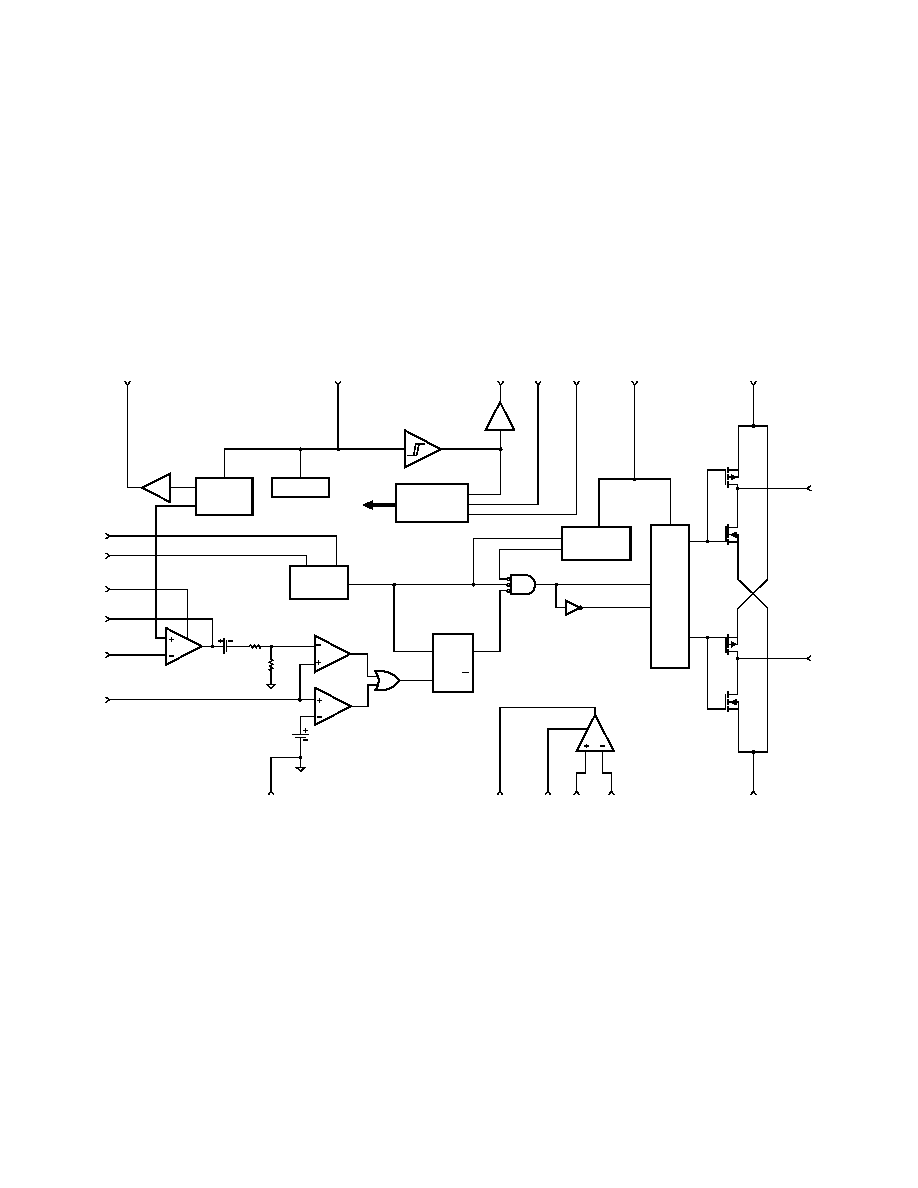
FIGURE 1 ≠ Block Diagram
Isense
VFB
Comp
SOFT
Rset
Cset
Error Amp
1.4V
VEE
AOUT
1V
Current Sense
Comparators
ENAUX
Internal Enable /
Shutdown Control
Lockout
SLEEP
EN
50%
PWROK
DRVP
OUTA
DRVN
Uncommited
Op-Amp
VCC
Undervoltage
VREF
OUTB
Output
Reference
Logic & Control
Functions
Duty Cycle
Limiting
(50% or 100%)
Drive
Internal Bias
S
R
Q
Q
Oscillator
PIN
NIN
12
15
16
14
13
22, 23
20
21
18,19
2
17
3
10
11
1,24
8
9
7
4
5
6

3
SCD5031 Rev B
Pr
el
im
in
ar
y
PWM5031 PWM PIN DESCRIPTION
PIN #
SIGNAL NAME
FUNCTION DESCRIPTION
1
24
VCC
Logic Power
2
50%
Input selects maximum duty cycle (50% or 100%). Logic ''1'' selects 50% max duty
cycle and Output B is the complement of Output A. Logic ''0'' selects 100% and
Output A is in-phase with Output B.
3
SLEEP
This Input shuts down all functions on chip when asserted (Active Hi)
4
COMP
Output of the error amplifier. Place compensation network from this pin to V
FB
to
stabilize converter.
5
VFB
Negative Input to the error amplifier
6
ISENSE
Input Current sense pin used for current mode control
7
SOFT
This High impedance Input is used to limit the error amplifier output voltage. Applying
an RC circuit to this pin provides the standard softstart function. Pull the pin to ground
to force zero duty cycle.
8
CSET
Works with Rset to establish oscillator free running frequency. Place cap from this
Input pin to ground. Can synchronize oscillator by overdriving this pin with an external
frequency source.
9
RSET
Works with Cset to establish oscillator free running frequency. Place resistor from this
Input pin to ground.
10
PWROK
Logical output of UV lockout circuit -- logic ''1'' indicates chip has valid Vcc
11
VREF
Buffered 3V Output reference voltage
12
VEE
Logic Ground
13
NIN
Auxiliary Op-Amp Inverting Input
14
PIN
Auxiliary Op-Amp Non-Inverting Input
15
AOUT
Auxiliary Op-Amp Output
16
ENAUX
Input Enable of Auxiliary Op-Amp (Active Hi)
17
EN
Logic Input that enables the oscillator and output drivers. Reference voltage remains
valid (Active Hi).
18
19
DRVN
Output stage negative rail
20
OUT B
Totem pole Output B
21
OUTA
Totem pole Output A
22
23
DRVP
Output stage positive rail
4
SCD5031 Rev B
Pr
el
im
in
ar
y
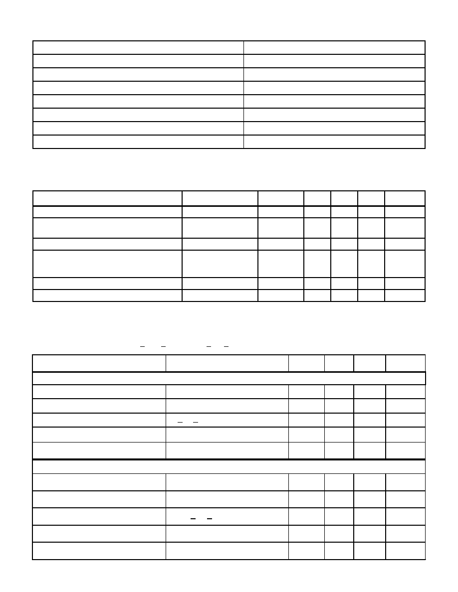
ABSOLUTE MAXIMUM RATINGS
1
Junction Temperature Range
-55∞C to +150∞C
Storage Temperature Range
-65∞C to +150∞C
V
CC
& DRVP Supply Voltages
7.0V
DC
Steady State Output Current
±50 mA
Peak Output Current (Internally Limited)
±1.0 A
Analog Inputs (Pins 5, 6, 13, 14)
V
EE
- 0.5V to V
CC
+ 0.5V
Power Dissipation at T
A
= +25∞C
500mW
Lead Temperature (soldering, 10 seconds)
300∞C
Note 1: All voltages are with respect to Pin 12. All currents are positive into the specified terminal.
OPERATING CONDITIONS
PARAMETER
CONDITION
SYMBOL
MIN
TYP
MAX
UNIT
DC Operating Voltage
-
V
CC
4.5
5.0
5.5
V
Quiescent Current
SLEEP @ '0';
EN & ENAUX @ '1'
I
CC
-
-
4.0
mA
Output Drive Voltage
-
DRVP
-
-
5.0
V
Output Duty Cycle ≠ Maximum
50% Pin = Logic 0
50% Pin = Logic 1
100% Duty Cycle
50% Duty Cycle
-
-
97*
-
-
-
-
50
%
%
Thermal Resistance T
JC
-
-
-
-
6.0
∞C/W
Sleep Mode
-
I
CCS
-
-
20
µA
* Dependent on Value of C
SET
& Operating Frequency
ELECTRICAL CHARACTERISTICS
4.5 V < Vcc < 5.5V, -55∞C < T
A
< +125∞C, unless otherwise specified
PARAMETER TEST
CONDITIONS
MIN
TYP
MAX
UNITS
Reference Section
Reference Voltage
T
A
= 25∞C, I
O
= -1 mA
2.95
3.05
3.15
V
Line Regulation
-
±.1
-
%
Load Regulation
0 < I
O
< 25 mA -
±.05
-
%
Thermal Regulation
-
±1
-
%
Output Short Circuit
Note 2
-
-
-40
mA
Oscillator Section
Frequency Range
Note 2
20
-
1,000
KHz
Frequency Stability (Part to Part)
Note 2
-
±1.5
±2
%
Temperature Stability
T
MIN
< T
A
< T
MAX
(Note 2)
-
±0.5
±1
%
R
SET
Range
Note 2
50
-
-
K
C
SET
Range
Note 2
-
-
600
pF

5
SCD5031 Rev B
Pr
el
im
in
ar
y
Error Amp Section
Input Offset Voltage
Note 2
-
-
3.3
mV
Input Common Mode Voltage Range
Note 2
V
EE
+ 0.2
-
V
CC
- 0.2
V
Input Bias Current
Note 2
-
-
-1.0
µA
Open Loop Voltage Gain (AVOL)
Note 2
100
-
-
dB
Unity Gain Bandwidth
Note 2
1.0
2.0
-
MHz
Power Supply Rejection Ratio (PSRR)
Note 2
60
-
-
dB
Output Sink Current
V
FB
= 3.0V, V
SOFT
= 1.1V
-
-
+62
mA
Output Source Current
V
FB
= 2.0V, V
SOFT
= 5V
-
-
-40
mA
V
OUT
High (Limited by V
SOFT
)
V
FB
= 2.0V, R
L
= 15K to GND
V
SOFT
-
0.2
-
-
V
V
OUT
Low
V
FB
= 3.0V, R
L
= 15K to +5V
-
-
V
EE
+ 0.2
V
Current Sense Section
Input Offset Voltage
Note 2
-
-
3.3
mV
Common Mode Input Voltage
V
SOFT
= 5V, Note 2 & 3
0.1
-
1.0
V
Input Bias Current
Note 2
-
-
1.0
µA
I
SENSE
to Output Delay
-
80
100
ns
Output Section
Output Low Level
I
SINK
= 1.0mA
-
-
0.1
V
I
SINK
= 50mApk
-
-
0.3
V
Output High Level
I
SOURCE
= 1.0mA, DRVP = 5V
4.9
-
-
V
I
SOURCE
= 50mApk, DRVP = 5V
4.7
-
-
V
Peak Output Current
-
±1.35
-
A
Steady State Output Current
-
50
-
mA
Rise Time
T
A
=
25∞C
,
C
L
=
1.0nF
-
8.0
-
ns
Fall Time
T
A
=
25∞C
,
C
L
=
1.0nF
-
6.0
-
ns
ELECTRICAL CHARACTERISTICS con't
4.5 V < Vcc < 5.5V, -55∞C < T
A
< +125∞C, unless otherwise specified
PARAMETER TEST
CONDITIONS
MIN
TYP
MAX
UNITS