 | –≠–ª–µ–∫—Ç—Ä–æ–Ω–Ω—ã–π –∫–æ–º–ø–æ–Ω–µ–Ω—Ç: AT-30511 | –°–∫–∞—á–∞—Ç—å:  PDF PDF  ZIP ZIP |
Document Outline
- List of Figures
- 1 Test Circuit for Noise Figure and Associated Gain. This Circuit is a Compromise Match Between Best Noise Figure, Best Gain, St
- 2. AT-30511 and AT-30533 Minimum Noise Figure and Amplifier NF [1] vs. Frequency and Current at VCE = 2.7V
- 3. AT-30511 Associated Gain at Optimum Noise Match vs. Frequency and Current at VCE = 2 .7 V
- 4 AT-30533 Associated Gain at Optimum Noise Match vs. Frequency and Current at VCE = 2 .7 V
- 5. AT-30511 and AT-30533 Power at 1 dB Gain Compression vs. Frequency and Current at VCE = 2.7 V
- 6. AT-30511 1 dB Compressed Gain vs. Frequency and Current at VCE = 2.7 V
- 7. AT-30533 1 dB Compressed Gain vs. Frequency and Current at VCE = 2.7 V
- 8. AT-30511 and AT-30533 Power at 1 dB Gain Compression vs. Frequency and Current at VCE = 5 V
- 9. AT-30511 1 dB Compressed Gain vs. Frequency and Current at VCE =5 V
- 10. AT-30533 1 dB Compressed Gain vs. Frequency and Current at VCE =5 V
- 11. AT-30511 and AT-30533 Power at 1 dB Gain Compression vs. Frequency and Current at V CE = 1 V
- 12. AT-30511 1 dB Compressed Gain vs. Frequency and Current at V CE =1V
- 13. AT-30533 1 dB Compressed Gain vs. Frequency and Current at V CE =1 V
- 14. AT-30511 Noise Figure and Associated Gain at V CE = 2.7 V, I C = 1 mA vs.TemperatureinTest Circuit, Figure 1. (Circuit
- 15. AT-30533 Noise Figure and Associated Gain at V CE = 2.7 V, I C = 1 mA vs.TemperatureinTest Circuit, Figure 1. (Circuit
- 16. AT-30511 and AT-30533 Intermodulation Products vs. Output PoweratV CE =2 .7V,I C = 10mA, 900 MHz with Optimal Tuning
- 17. AT-30511 Gains vs. Frequency at V CE = 1 V, I C = 1 mA
- 18. AT-30533 Gains vs. Frequency at V CE = 2 .7 V, I C = 1 mA
- 19. AT-30511 Gains vs. Frequency at VCE = 2 .7 V, IC = 1 mA
- 20. AT-30511- Gains vs. Frequency at VCE = 2 .7 V, IC = 1 mA
- 21. AT-30511 Gains vs. Frequency at VCE = 2.7 V, IC = 5 mA
- 22. AT-30533 Gains vs. Frequency at VCE = 2 .7 V, IC = 5 mA
- 23. AT-30511 Gains vs. Frequency at V CE = 5 V, I C = 1 mA
- 24. AT-30533 Gains vs. Frequency at V CE = 5 V, I C = 1 mA
- 25. AT-30511 Gains vs. Frequency at VCE = 5 V, IC = 5 mA
- 26. AT-30533 Gains vs. Frequency at VCE = 5 V, IC = 5 mA
- Features
- Outline Drawing
- Description
- AT-30511, AT-30533 Absolute Maximum Ratings
- Electrical Specifications, T A = 25∞C
- AT-30511, AT-30533 Characterization Information, T A = 25∞C
- Typical Performance
- AT-30511 Typical Scattering Parameters
- AT-30511 Typical Noise Parameters
- AT-30533 Typical Scattering Parameters, VCE = 1 V, IC = 1 mA, Common Emitter, ZO = 50 W
- AT-30533 Typical Noise Parameters,
- AT-30511 Typical Scattering Parameters,
- AT-30511 Typical Noise Parameters,
- AT-30533 Typical Scattering Parameters,
- AT-30533 Typical Noise Parameters,
- AT-30511 Typical Scattering Parameters,
- AT-30511 Typical Noise Parameters,
- AT-30533 Typical Scattering Parameters,
- AT-30533 Typical Noise Parameters,
- AT-30511 Typical Scattering Parameters,
- AT-30511 Typical Noise Parameters,
- AT-30533 Typical Scattering Parameters,
- AT-30533 Typical Noise Parameters,
- AT-30511 Typical Scattering Parameters,
- AT-30511 Typical Noise Parameters,
- AT-30533 Typical Scattering Parameters,
- AT-30533 Typical Noise Parameters,
- Ordering Information
- Package Dimensions
- SOT-143 Plastic Package
4-23
Low Current, High Performance
NPN Silicon Bipolar Transistor
Technical Data
Description
Hewlett-Packard's AT-30511 and
AT-30533 are high performance
NPN bipolar transistors that have
been optimized for maximum f
T
at
low voltage operation, making
them ideal for use in battery
powered applications in wireless
markets. The AT-30533 uses the 3
lead SOT-23, while the AT-30511
places the same die in the higher
performance 4 lead SOT-143. Both
packages are industry standard,
and compatible with high volume
surface mount assembly
techniques.
The 3.2 micron emitter-to-emitter
pitch and reduced parasitic design
of these transistors yields
extremely high performance
products that can perform a multi-
plicity of tasks. The 5 emitter
finger interdigitated geometry
yields an extremely fast transistor
with high gain and low operating
currents.
Features
∑ High Performance Bipolar
Transistor Optimized for
Low Current, Low Voltage
Operation
∑ 900 MHz Performance:
AT-30511: 1.1 dB NF, 16 dB G
A
AT-30533: 1.1 dB NF, 13 dB G
A
∑ Characterized for End-Of-
Life Battery Use (2.7 V)
∑ SOT-23 and SOT-143 SMT
Plastic Packages
∑ Tape-And-Reel Packaging
Option Available
[1]
Optimized performance at 2.7 V
makes these devices ideal for use
in 900 MHz, 1.8 GHz, and 2.4 GHz
battery operated systems as an
LNA, gain stage, buffer, oscillator,
or active mixer. Typical amplifier
designs at 900 MHz yield 1.3 dB
noise figures with 13 dB or more
associated gain at a 2.7 V, 1 mA
bias. Voltage breakdowns are high
enough for use at 5 volts. High
gain capability at 1 V, 1 mA makes
these devices a good fit for
900 MHz pager applications.
The AT-3 series bipolar transistors
are fabricated using an optimized
version of Hewlett- Packard's
10 GHz f
T
, 30 GHz f
MAX
Self-
Aligned-Transistor (SAT) process.
The die are nitride passivated for
surface protection. Excellent
device uniformity, performance
and reliability are produced by the
use of ion-implantation, self-
alignment techniques, and gold
metalization in the fabrication of
these devices.
AT-30511
AT-30533
Outline Drawing
Note:
1. Refer to "Tape-and-Reel Packaging for
Semiconductor Devices".
BASE
EMITTER
EMITTER COLLECTOR
BASE
EMITTER
COLLECTOR
305
305
SOT-23 (AT-30533)
SOT-143 (AT-30511)
5965-8918E
4-24
AT-30511, AT-30533 Absolute Maximum Ratings
Symbol
Parameter
Units
Absolute Maximum
[1]
V
EBO
Emitter-Base Voltage
V
1.5
V
CBO
Collector-Base Voltage
V
11
V
CEO
Collector-Emitter Voltage
V
5.5
I
C
Collector Current
mA
8
P
T
Power Dissipation
[2] [3]
mW
100
T
j
Junction Temperature
∞
C
150
T
STG
Storage Temperature
∞
C
-65 to 150
Notes:
1. Operation of this device above any one of these parameters may cause permanent
damage.
2. T
Mounting Surface
= 25
∞
C.
3. Derate at 1.82 mW/
∞
C for T
C
> 95
∞
C.
Thermal Resistance
[2]
:
jc
= 550
∞
C/W
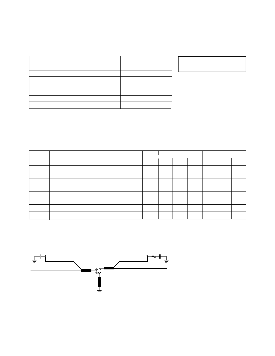
Figure 1. Test Circuit for Noise Figure and Associated Gain. This Circuit is a
Compromise Match Between Best Noise Figure, Best Gain, Stability, a Practical,
Synthesizable Match, and a Circuit Capable of Matching Both the AT-305 and
AT-310 Geometries.
1000 pF
V
BB
W = 10 L = 1860
W = 10 L = 1000
W = 30 L = 100
W = 30 L = 100
W = 10 L = 1860
1000 pF
V
CC
25
W = 10 L = 1025
TEST CIRCUIT A: W = 20 L = 100
TEST CIRCUIT B: W = 20 L = 200 x 2
NOT TO SCALE
TEST CIRCUIT
BOARD MATL = 0.062" FR-4 (
= 4.8)
DIMENSIONS IN MILS
Electrical Specifications, T
A
= 25
∞
C
AT-30511
AT-30533
Symbol
Parameters and Test Conditions
Units
Min
Typ
Max
Min
Typ
Max
NF
Noise Figure
V
CE
= 2.7 V, I
C
= 1 mA
f = 0.9 GHz
dB
1.1
[1]
1.4
[1]
1.1
[2]
1.4
[2]
G
A
Associated Gain
V
CE
= 2.7 V, I
C
= 1 mA
f = 0.9 GHz
dB
14
[1]
16
[1]
11
[2]
13
[2]
h
FE
Forward Current
V
CE
= 2.7 V
-
70
300
70
300
Transfer Ratio
I
C
= 1 mA
I
CBO
Collector Cutoff Current
V
CB
= 3 V
µ
A
0.03
0.2
0.03
0.2
I
EBO
Emitter Cutoff Current
V
EB
= 1 V
µ
A
0.1
1.5
0.1
1.5
Notes:
1. Test circuit B, Figure 1. Numbers reflect device performance de-embedded from circuit losses.
Input loss = 0.4 dB; output loss = 0.4 dB.
2. Test circuit A, Figure 1. Numbers reflect device performance de-embedded from circuit losses.
Input loss = 0.4 dB; output loss = 0.4 dB.
4-25
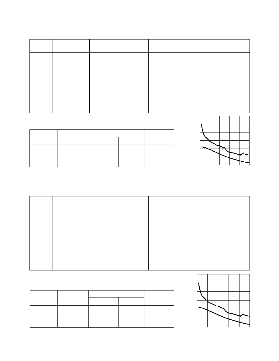
AT-30511, AT-30533 Characterization Information, T
A
= 25
∞
C
AT-30511 AT-30533
Symbol
Parameters and Test Conditions
Units
Typ
Typ
P
1dB
Power at 1 dB Gain Compression (opt tuning)
V
CE
= 2.7 V, I
C
= 5 mA
f = 0.9 GHz
dBm
7
7
G
1dB
Gain at 1 dB Gain Compression (opt tuning)
V
CE
= 2.7 V, I
C
= 5 mA
f = 0.9 GHz
dB
16.5
15
IP
3
Output Third Order Intercept Point,
V
CE
= 2.7 V, I
C
= 5 mA (opt tuning)
f = 0.9 GHz
dBm
17
17
|S
21
|
E
2
Gain in 50
System; V
CE
= 2.7 V, I
C
= 1 mA
f = 0.9 GHz
dB
10
9
C
CB
Collector-Base Capacitance
V
CB
= 3V, f = 1 MHz
pF
0.04
0.04
P 1dB (dBm)
0
0
FREQUENCY (GHz)
1.0
1.5
10
4
2
0.5
2.5
6
2.0
8
5 mA
2 mA
G 1dB (dBm)
0
0
FREQUENCY (GHz)
1.0
1.5
25
10
5
0.5
2.5
15
2.0
20
5 mA
2 mA
G 1dB (dBm)
0
0
FREQUENCY (GHz)
1.0
1.5
25
10
5
0.5
2.5
15
2.0
20
5 mA
2 mA
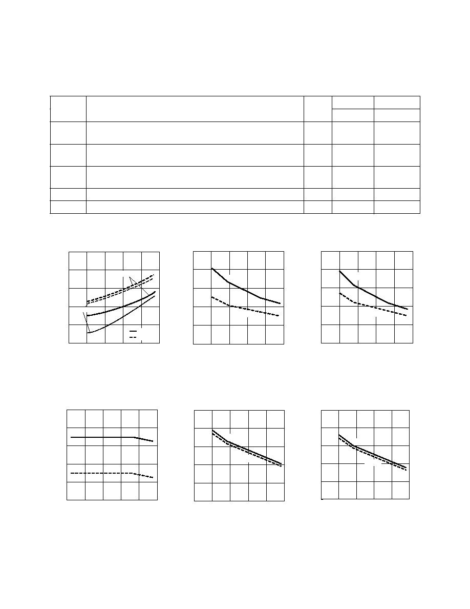
Typical Performance
Note:
1. Amplifier NF represents the noise figure which can be expected in a real circuit representing reasonable reflection coefficients and
including circuit losses.
Figure 7. AT-30533 1 dB Compressed
Gain vs. Frequency and Current at
V
CE
= 2.7 V.
Figure 6. AT-30511 1 dB Compressed
Gain vs. Frequency and Current at
V
CE
= 2.7 V.
Figure 5. AT-30511 and AT-30533
Power at 1 dB Gain Compression vs.
Frequency and Current at V
CE
= 2.7 V.
Figure 4. AT-30533 Associated Gain at
Optimum Noise Match vs. Frequency
and Current at V
CE
= 2 .7 V.
Figure 3. AT-30511 Associated Gain at
Optimum Noise Match vs. Frequency
and Current at V
CE
= 2 .7 V.
Figure 2. AT-30511 and AT-30533
Minimum Noise Figure and Amplifier
NF
[1]
vs. Frequency and Current at
V
CE
= 2 .7 V.
NOISE FIGURE (dB)
0
0
FREQUENCY (GHz)
1.0
1.5
2.5
1.0
0.5
0.5
2.5
1.5
2.0
2.0
1 mA
5 mA
AMPLIFIER NF
NF MIN.
Ga (dB)
0
0
FREQUENCY (GHz)
1.0
1.5
25
10
5
0.5
2.5
15
2.0
20
5 mA
1 mA
Ga (dB)
0
0
FREQUENCY (GHz)
1.0
1.5
25
10
5
0.5
2.5
15
2
20
5 mA
1 mA
4-26
P 1dB (dBm)
0
-4
FREQUENCY (GHz)
1.0
1.5
6
0
-2
0.5
2.5
2
2.0
4
2 mA
5 mA
G 1dB (dBm)
0
0
FREQUENCY (GHz)
1.0
1.5
25
10
5
0.5
2.5
15
2.0
20
5 mA
2 mA
G 1dB (dBm)
0
0
FREQUENCY (GHz)
1.0
1.5
25
10
5
0.5
2.5
15
2.0
20
5 mA
2 mA
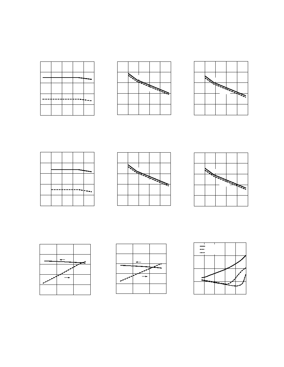
Figure 13. AT-30533 1 dB Compressed
Gain vs. Frequency and Current at
V
CE
= 1 V.
Figure 12. AT-30511 1 dB Compressed
Gain vs. Frequency and Current at
V
CE
= 1 V.
Figure 11. AT-30511 and AT-30533
Power at 1 dB Gain Compression vs.
Frequency and Current at V
CE
= 1 V.
AT-30511, AT-30533 Typical Performance,
continued
P 1dB (dBm)
0
0
FREQUENCY (GHz)
1.0
1.5
10
4
2
0.5
2.5
6
2.0
8
2 mA
5 mA
Figure 8. AT-30511 and AT-30533
Power at 1 dB Gain Compression vs.
Frequency and Current at V
CE
= 5 V.
Figure 9. AT-30511 1 dB Compressed
Gain vs. Frequency and Current at
V
CE
= 5 V.
Figure 10. AT-30533 1 dB Compressed
Gain vs. Frequency and Current at
V
CE
= 5 V.
G 1dB (dBm)
0
0
FREQUENCY (GHz)
1.0
1.5
25
10
5
0.5
2.5
15
2.0
20
5 mA
2 mA
G 1dB (dBm)
0
0
FREQUENCY (GHz)
1.0
1.5
25
10
5
0.5
2.5
15
2.0
20
5 mA
2 mA
Ga (dBm)
-50
0
TEMPERATURE (∞C)
50
25
10
5
0
100
15
20
0
2.5
1.0
0.5
1.5
2.0
NOISE FIGURE (dB)
Ga
NF
Ga (dBm)
-50
0
TEMPERATURE (∞C)
50
25
10
5
0
100
15
20
0
2.5
1.0
0.5
1.5
2.0
NOISE FIGURE (dB)
Ga
NF
IM3 (dBc)
-9
-80
POWER PER TONE (dBm)
-3
0
0
-60
-6
6
-40
3
-20
IM3 (dBc)
IM5 (dBc)
IM7 (dBc)
Figure 14. AT-30511 Noise Figure and
Associated Gain at V
CE
= 2.7 V,
I
C
= 1 mA vs. Temperature in Test
Circuit, Figure 1. (Circuit Losses
De-embedded)
Figure 16. AT-30511 and AT-30533
Intermodulation Products vs. Output
Power at V
CE
= 2 .7 V, I
C
= 10 mA,
900 MHz with Optimal Tuning.
Figure 15. AT-30533 Noise Figure and
Associated Gain at V
CE
= 2.7 V,
I
C
= 1 mA vs. Temperature in Test
Circuit, Figure 1. (Circuit Losses
De-embedded)
4-27
AT-30533 Typical Noise Parameters,
Common Emitter, Z
O
= 50
, 1 V, I
C
= 1 mA
OPT
Freq
F
min
[1]
R
n
GHz
dB
Mag
Ang
0.5
[2]
0.3
0.94
7
1.02
0.9
0.4
0.89
16
0.86
1.8
0.9
0.75
43
0.58
2.4
1.3
0.65
65
0.38
Notes:
1. Matching constraints may make F
min
values associated with high |
opt
| values
unachievable in physical circuits. See Fig. 2 for expected performance.
2. 0.5 GHz noise parameter values are extrapolated, not measured.
AT-30511 Typical Noise Parameters,
Common Emitter, Z
O
= 50
, 1 V, I
C
= 1 mA
OPT
Freq
F
min
[1]
R
n
GHz
dB
Mag
Ang
0.5
[2]
0.3
0.96
10
1.49
0.9
0.4
0.92
19
1.33
1.8
0.9
0.83
43
0.98
2.4
1.3
0.76
60
0.74
Notes:
1. Matching constraints may make F
min
values associated with high |
opt
| values
unachievable in physical circuits. See Fig. 2 for expected performance.
2. 0.5 GHz noise parameter values are extrapolated, not measured.
AT-30533 Typical Scattering Parameters,
V
CE
= 1 V, I
C
= 1 mA
,
Common Emitter, Z
O
= 50
Freq.
S
11
S
21
S
12
S
22
GHz
Mag
Ang
dB
Mag
Ang
dB
Mag
Ang
Mag
Ang
0.1
0.95
-5
10.90
3.51
174
-38.36
0.01
87
0.99
-3
0.5
0.91
-25
10.32
3.28
150
-25.08
0.06
73
0.95
-14
0.9
0.77
-41
9.44
2.97
128
-20.95
0.09
63
0.89
-24
1.0
0.73
-45
9.03
2.83
124
-20.21
0.10
61
0.88
-25
1.5
0.55
-62
7.75
2.44
102
-18.13
0.12
54
0.80
-33
1.8
0.46
-71
6.94
2.22
91
-17.33
0.14
51
0.77
-36
2.0
0.41
-76
6.51
2.12
85
-16.84
0.14
50
0.74
-38
2.4
0.30
-85
5.45
1.87
73
-16.05
0.16
49
0.71
-41
3.0
0.17
-95
4.26
1.63
57
-14.80
0.18
49
0.68
-46
4.0
0.02
-139
2.71
1.37
37
-12.58
0.24
48
0.65
-57
5.0
0.12
61
1.56
1.20
19
-10.14
0.31
45
0.62
-69
AT-30511 Typical Scattering Parameters,
V
CE
= 1 V, I
C
= 1 mA, Common Emitter, Z
O
= 50
Freq.
S
11
S
21
S
12
S
22
GHz
Mag
Ang
dB
Mag
Ang
dB
Mag
Ang
Mag
Ang
0.1
0.97
-5
10.84
3.48
175
-39.42
0.01
86
0.99
-2
0.5
0.95
-24
10.51
3.35
155
-25.87
0.05
72
0.95
-14
0.9
0.85
-42
9.96
3.15
137
-21.46
0.08
61
0.92
-24
1.0
0.83
-46
9.66
3.04
133
-20.71
0.09
58
0.91
-26
1.5
0.70
-67
8.71
2.73
113
-18.44
0.12
46
0.84
-36
1.8
0.63
-78
8.06
2.53
102
-17.69
0.13
41
0.80
-40
2.0
0.59
-85
7.75
2.44
96
-17.27
0.14
37
0.77
-43
2.4
0.50
-100
6.73
2.17
84
-16.79
0.14
32
0.73
-48
3.0
0.39
-122
5.58
1.90
67
-16.32
0.15
27
0.68
-53
4.0
0.29
-161
3.97
1.58
45
-15.87
0.16
20
0.63
-63
5.0
0.27
153
2.64
1.36
25
-15.47
0.17
20
0.61
-72
GAIN (dB)
0
0
FREQUENCY (GHz)
2
3
30
1
5
10
4
20
MSG
MAG
S21
MSG
Figure 17. AT-30511 Gains vs.
Frequency at V
CE
= 1 V, I
C
= 1 mA.
GAIN (dB)
0
0
FREQUENCY (GHz)
2
3
30
1
5
10
4
20
MSG
MAG
S21
MSG
Figure 18. AT-30533 Gains vs.
Frequency at V
CE
= 2 .7 V, I
C
= 1 mA.