 | –≠–ª–µ–∫—Ç—Ä–æ–Ω–Ω—ã–π –∫–æ–º–ø–æ–Ω–µ–Ω—Ç: AT-41411 | –°–∫–∞—á–∞—Ç—å:  PDF PDF  ZIP ZIP |
Document Outline
- List of Figures
- 1. Noise Figure and Associated Gain vs. Frequency. V CE = 8 V, I C =10mA
- 2. Optimum Noise Figure and Associated Gain vs. Collector Current and Frequency. V CE = 8 V, f = 2.0 GHz
- 3. Insertion Power Gain vs. Collector Current and Frequency V CE = 8 V
- 4. Insertion Power Gain, Maximum Available Gain and Maximum Stable Gain vs. Frequency V CE = 8 V, I C = 20 mA
- Features
- Description
- SOT-143 Plastic
- Pin Connections
- AT-41411 Absolute Maximum Ratings
- Part Number Ordering Information
- Electrical Specifications, TA = 25∞C
- AT-41411 Typical Performance, TA = 25∞C
- AT-41411 Typical Scattering Parameters,
- AT-41411 Typical Scattering Parameters,
- AT-41411 Noise Parameters:
- SOT-143 Plastic Dimensions

4-109
Surface Mount Low Noise
Silicon Bipolar Transistor Chip
Technical Data
Features
∑ Low Noise Figure:
1.4 dB Typical at 1.0 GHz
1.8 dB Typical at 2.0 GHz
∑ High Associated Gain:
18.0 dB Typical at 1.0 GHz
13.0 dB Typical at 2.0 GHz
∑ High Gain-Bandwidth
Product: 7.0 GHz Typical f
T
∑ Low Cost Surface Mount
Plastic Package
∑ Tape-and-Reel Packaging
Option Available
[1]
AT-41411
SOT-143 Plastic
Note:
1. Refer to "Tape-and-Reel Packaging for
Semiconductor Devices".
Description
Hewlett-Packard's AT-41411 is a
general purpose NPN bipolar
transistor that offers excellent
high frequency performance. The
AT-41411 is housed in a low cost
low parasitic 4 lead SOT-143
surface mount package. The
SOT-143 is an industry standard
and is compatible with high
volume surface mount assembly
techniques. The 4 micron emitter-
to-emitter pitch enables this
transistor to be used in many
different functions. The 14 emitter
finger interdigitated geometry
yields an intermediate sized
transistor with impedances that
are easy to match for low noise
and moderate power applications.
This device is designed for use in
low noise, wideband amplifier,
mixer and oscillator applications
in the VHF, UHF, and microwave
frequencies. An optimum noise
match near 50
in the 1 to 2 GHz
frequency range, makes this
device easy to use as a low noise
amplifier.
The AT-41411 bipolar transistor is
fabricated using Hewlett-Packard's
10 GHz f
T
Self-Aligned-Transistor
(SAT) process. The die is nitride
passivated for surface protection.
Excellent device uniformity,
performance and reliability are
produced by the use of ion-
implantation, self-alignment
techniques, and gold metalization
in the fabrication of this device.
Pin Connections
GND
OUTPUT
INPUT
V
CC
414
5965-8924E
4-110
AT-41411 Absolute Maximum Ratings
Absolute
Symbol
Parameter
Units
Maximum
[1]
V
EBO
Emitter-Base Voltage
V
1.5
V
CBO
Collector-Base Voltage
V
20
V
CEO
Collector-Emitter Voltage
V
12
I
C
Collector Current
mA
50
P
T
Power Dissipation
[2,3]
mW
225
T
j
Junction Temperature
∞
C
150
T
STG
Storage Temperature
∞
C
-65 to 150
Thermal Resistance
[2,4]
:
jc
= 550
∞
C/W
Notes:
1. Permanent damage may occur if
any of these limits are exceeded.
2. T
CASE
= 25
∞
C.
3. Derate at 1.8 mW/
∞
C for T
C
> 26
∞
C.
4. See MEASUREMENTS section
"Thermal Resistance" for more
information.
Part Number Ordering Information
Part Number
Increment
Comments
AT-41411-TR1
3000
Reel
AT-41411-BLK
100
Bulk
Note:
For more information, see "Tape and Reel Packaging for Semiconductor Devices".
Electrical Specifications, T
A
= 25
∞
C
Symbol
Parameters and Test Conditions
[1]
Units Min.
Typ. Max.
|S
21E
|
2
Insertion Power Gain; V
CE
= 8 V, I
C
= 20 mA
f = 1.0 GHz
dB
14.5
16.5
f = 2.0 GHz
11.0
P
1 dB
Power Output @ 1 dB Gain Compression
f = 2.0 GHz
dBm
17.0
V
CE
= 8 V, I
C
= 20 mA
G
1 dB
1 dB Compressed Gain; V
CE
= 8 V, I
C
= 20 mA
f = 2.0 GHz
dB
13.0
NF
O
Optimum Noise Figure: V
CE
= 8 V, I
C
= 10 mA
f = 1.0 GHz
dB
1.4
f = 2.0 GHz
1.8
f = 4.0 GHz
3.5
G
A
Gain @ NF
O
; V
CE
= 8 V, I
C
= 10 mA
f = 1.0 GHz
dB
18.0
f = 2.0 GHz
13.0
f = 4.0 GHz
9.0
f
T
Gain Bandwidth Product: V
CE
= 8 V, I
C
= 20 mA
GHz
7.0
h
FE
Forward Current Transfer Ratio; V
CE
= 8 V, I
C
= 10 mA
--
30
150
270
I
CBO
Collector Cutoff Current; V
CB
= 8 V
µ
A
0.2
I
EBO
Emitter Cutoff Current; V
EB
= 1 V
µ
A
1.0
Notes:
1. Refer to PACKAGING Section, "Tape-and-Reel Packaging for Semiconductor Devices."
4-111
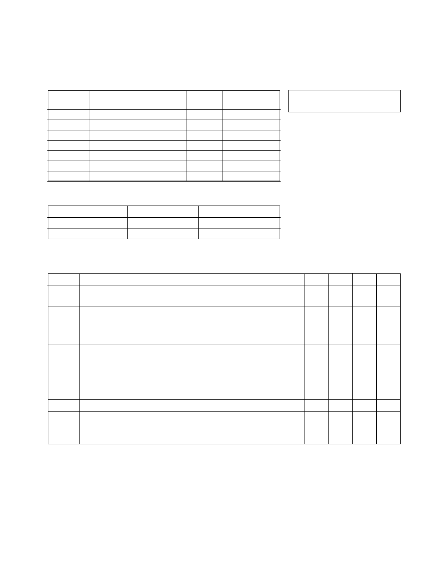
AT-41411 Typical Performance, T
A
= 25
∞
C
FREQUENCY (GHz)
GAIN (dB)
I
C
(mA)
Figure 2. Optimum Noise Figure and
Associated Gain vs. Collector Current
and Frequency. V
CE
= 8 V, f = 2.0 GHz.
Figure 1. Noise Figure and Associated
Gain vs. Frequency. V
CE
= 8 V,
I
C
=10mA.
GAIN (dB)
0
10
20
30
FREQUENCY (GHz)
Figure 4. Insertion Power Gain,
Maximum Available Gain and
Maximum Stable Gain vs. Frequency.
V
CE
= 8 V, I
C
= 20 mA.
GAIN (dB)
0.1
0.5
0.3
1.0
3.0
6.0
24
21
18
15
12
9
6
3
0
4
2
0
NF
O
(dB)
4
2
0
NF
O
(dB)
0.5
2.0
1.0
3.0
4.0
16
14
12
10
GA
GA
NFO
NFO
I
C
(mA)
Figure 3. Insertion Power Gain vs.
Collector Current and Frequency.
V
CE
= 8 V.
20
16
12
8
4
0
|S
21E
|
2
GAIN (dB)
0
10
20
30
2.0 GHz
4.0 GHz
40
35
30
25
20
15
10
5
0
MSG
MAG
|S21E|
2
1.0 GHz

4-112
AT-41411 Typical Scattering Parameters,
Common Emitter, Z
O
= 50
, T
A
= 25
∞
C, V
CE
= 8 V, I
C
= 10 mA
Freq.
S
11
S
21
S
12
S
22
GHz
Mag.
Ang.
dB
Mag.
Ang.
dB
Mag.
Ang.
Mag.
Ang.
0.1
.85
-30
27.3
23.20
158
-37.7
.013
64
.93
-11
0.5
.58
-112
21.7
12.18
109
-29.1
.035
44
.62
-30
1.0
.49
-156
16.5
6.70
85
-27.2
.044
43
.50
-33
1.5
.49
178
13.2
4.58
71
-25.0
.056
47
.46
-36
2.0
.50
160
10.8
3.45
59
-23.4
.068
47
.45
-41
2.5
.53
153
9.0
2.82
53
-22.5
.075
56
.43
-43
3.0
.55
142
7.5
2.37
43
-21.0
.089
54
.43
-53
3.5
.56
133
6.1
2.02
33
-19.8
.102
52
.44
-63
4.0
.56
121
4.9
1.76
23
-18.8
.115
49
.46
-73
AT-41411 Typical Scattering Parameters,
Common Emitter, Z
O
= 50
, T
A
= 25
∞
C, V
CE
= 8 V, I
C
= 20 mA
Freq.
S
11
S
21
S
12
S
22
GHz
Mag.
Ang.
dB
Mag.
Ang.
dB
Mag.
Ang.
Mag.
Ang.
0.1
.65
-46
30.4
33.07
150
-40.0
.010
59
.89
-15
0.5
.46
-137
22.4
13.21
100
-32.0
.025
56
.57
-26
1.0
.43
-175
16.7
6.85
80
-28.4
.038
58
.52
-29
1.5
.44
163
13.3
4.63
67
-26.4
.048
61
.51
-32
2.0
.47
148
10.8
3.47
56
-24.2
.062
61
.50
-37
2.5
.50
140
9.0
2.82
50
-22.9
.071
60
.47
-39
3.0
.53
132
7.5
2.36
40
-20.7
.092
61
.46
-48
3.5
.55
122
6.1
2.02
30
-19.6
.105
57
.45
-60
4.0
.56
112
4.8
1.74
19
-18.3
.122
53
.45
-73
A model for this device is available in the DEVICE MODELS section.
AT-41411 Noise Parameters:
V
CE
= 8 V, I
C
= 10 mA
Freq.
NF
O
opt
GHz
dB
Mag
Ang
R
N
/50
0.1
1.3
.12
4
0.17
0.5
1.3
.10
23
0.17
1.0
1.4
.07
57
0.16
2.0
1.8
.09
-158
0.16
4.0
3.5
.31
-87
0.38
4-113
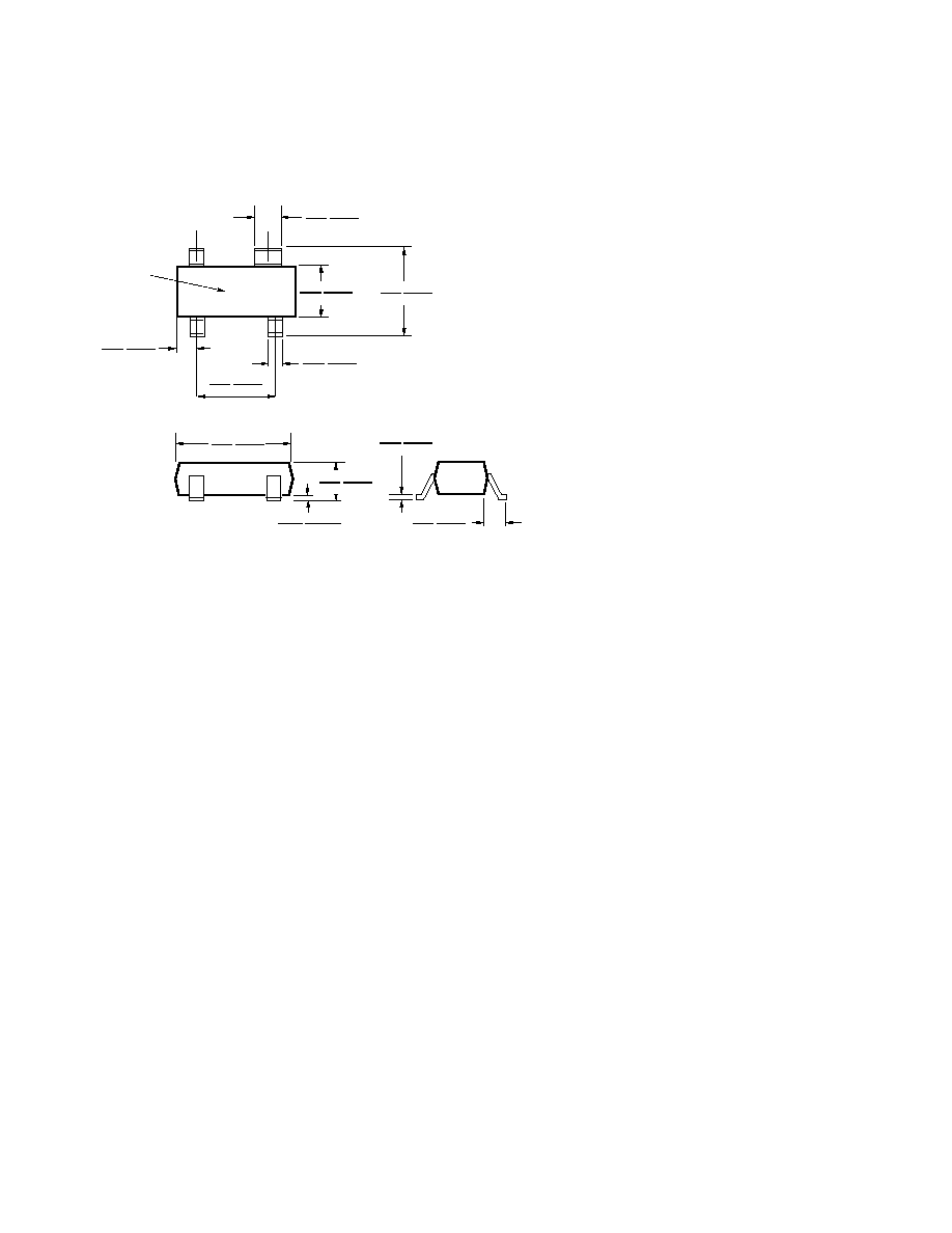
SOT-143 Plastic Dimensions
DIMENSIONS ARE IN MILLIMETERS (INCHES)
0.10 (0.004)
0.013 (0.0005)
3.06 (0.120)
2.80 (0.110)
1.02 (0.041)
0.85 (0.033)
0.92 (0.036)
0.78 (0.031)
E
E
B
C
XXX
PACKAGE
MARKING
CODE
1.40 (0.055)
1.20 (0.047)
2.65 (0.104)
2.10 (0.083)
0.54 (0.021)
0.37 (0.015)
0.60 (0.024)
0.45 (0.018)
2.04 (0.080)
1.78 (0.070)
TOP VIEW
0.15 (0.006)
0.09 (0.003)
0.69 (0.027)
0.45 (0.018)
END VIEW
SIDE VIEW