 | –≠–ª–µ–∫—Ç—Ä–æ–Ω–Ω—ã–π –∫–æ–º–ø–æ–Ω–µ–Ω—Ç: AT41511 | –°–∫–∞—á–∞—Ç—å:  PDF PDF  ZIP ZIP |
Document Outline
- List of Figures
- 1. AT-41511 and AT-41533 Minimum Noise Figure vs. Frequency and Current at V CE = 2.7 V.
- 2. AT-41511 and AT-41533 Minimum Noise Figure vs. Frequency and Current at V CE = 5 V.
- 3. AT-41511 and AT-41533 Minimum Noise Figure vs. Frequency and Current at V CE = 8 V.
- 4. AT-41511 and AT-41533 Associated Gain vs. Frequency and Current at V CE = 2.7 V.
- 5. AT-41511 and AT-41533 Associated Gain vs. Frequency and Current at V CE = 5 V.
- 6. AT-41511 and AT-41533 Associated Gain vs. Frequency and Current at V CE = 8 V.
- 7. AT-41511 and AT-41533 P 1dB vs. Frequency and Bias at V CE=2.7 V, with Optimal Tuning.
- 8. AT-41511 and AT-41533 P 1dB vs. Frequency and Bias at V CE = 5 V, with Optimal Tuning.
- 9. AT-41511 and AT-41533 P 1dB vs. Frequency and Bias at V CE = 8 V, with Optimal Tuning.
- 10. AT-41511 Gains vs. Frequency at V CE = 2.7 V, I C = 5 mA.
- 11. AT-41533 Gains vs. Frequency at V CE = 2.7 V, I C = 5 mA.
- 12. AT-41511 Gains vs. Frequency at V CE = 2.7 V, I C = 25 mA.
- 13. AT-41533 Gains vs. Frequency at V CE = 2.7 V, I C = 25 mA.
- 14. AT-41511 Gains vs. Frequency at V CE = 5 V, I C = 5 mA.
- 15. AT-41533 Gains vs. Frequency at V CE = 5 V, I C = 5 mA.
- 16. AT-41511 Gains vs. Frequency at V CE = 5 V, I C = 25 mA.
- 17. AT-41533 Gains vs. Frequency at V CE = 5 V, I C = 25 mA.
- 18. AT-41511 Gains vs. Frequency at V CE = 8 V, I C = 10 mA.
- 19. AT-41533 Gains vs. Frequency at V CE = 8 V, I C = 10 mA.
- 20. AT-41511 Gains vs. Frequency at Vce = 8, Ic=25 mA
- 21. AT-41533 Gains vs. Frequency at Vce=8 V, Ic=25 mA
- Features
- Outline Drawing
- Description
- AT-41511, AT-41533 Absolute Maximum Ratings
- Electrical Specifications, T A = 25∞C
- Characterization Information, T A = 25∞C
- Ordering Information
- AT-41511, AT-41533 Typical Performance
- AT-41511 Typical Scattering Parameters, Common Emitter, Z o = 50 W, V CE = 2.7 V, I C = 5 mA
- AT-41511 Typical Noise Parameters,
- AT-41533 Typical Scattering Parameters, Common Emitter, Z o = 50 W, V CE = 2.7 V, I C = 5 mA
- AT-41533 Typical Noise Parameters,
- AT-41511 Typical Scattering Parameters, Common Emitter, Z o = 50 W, V CE = 2.7 V, I C = 25 mA
- AT-41511 Typical Noise Parameters,
- AT-41533 Typical Scattering Parameters, Common Emitter, Z o = 50 W, V CE = 2.7 V, I C = 25 mA
- AT-41533 Typical Noise Parameters,
- AT-41511 Typical Scattering Parameters, Common Emitter, Z o = 50 W, V CE = 5 V, I C = 5 mA
- AT-41511 Typical Noise Parameters,
- AT-41533 Typical Scattering Parameters, Common Emitter, Z o = 50 W, V CE = 5 V, I C = 5 mA
- AT-41533 Typical Noise Parameters,
- AT-41511 Typical Scattering Parameters, Common Emitter, Z o = 50 W, V CE = 5 V, I C = 25 mA
- AT-41511 Typical Noise Parameters,
- AT-41533 Typical Scattering Parameters, Common Emitter, Z o = 50 W, V CE = 5 V, I C = 25 mA
- AT-41533 Typical Noise Parameters,
- AT-41511 Typical Scattering Parameters, Common Emitter, Z o = 50 W, V CE = 8 V, I C = 10 mA
- AT-41511 Typical Noise Parameters,
- AT-41533 Typical Scattering Parameters, Common Emitter, Z o = 50 W, V CE = 8 V, I C = 10 mA
- AT-41533 Typical Noise Parameters,
- AT-41511 Typical Scattering Parameters, Common Emitter, Z o = 50 W, V CE = 8 V, I C = 25 mA
- AT-41511 Typical Noise Parameters,
- AT-41533 Typical Scattering Parameters, Common Emitter, Z o = 50 W, V CE = 8 V, I C = 25 mA
- AT-41533 Typical Noise Parameters, Common Emitter, Zo=50, Vce= 8 V, Ic =25 mA
- Package Dimensions SOT-143 Plastic Package
- SOT-23 Plastic Package
4-134
General Purpose, Low Noise
NPN Silicon Bipolar Transistor
Technical Data
Features
∑ General Purpose NPN
Bipolar Transistor
∑ 900 MHz Performance:
AT-41511: 1 dB NF, 15.5 dB G
A
AT-41533: 1 dB NF, 14.5 dB G
A
∑ Characterized for 3, 5, and
8 Volt Use
∑ SOT-23 and SOT-143 SMT
Plastic Packages
∑ Tape-and-Reel Packaging
Option Available
[1]
Description
Hewlett-Packard's AT-41511 and
AT-41533 are general purpose
NPN bipolar transistors that offer
excellent high frequency
performance at an economical
price. The AT-41533 uses the
3 lead SOT-23, while the AT-415 11
places the same die in the lower
parasitic 4 lead SOT-143. Both
packages are industry standard,
and compatible with high volume
surface mount assembly
techniques.
The 4 micron emitter-to-emitter
pitch of these transistors yields
high performance products that
can perform a multiplicity of
tasks. The 14 emitter finger
interdigitated geometry yields an
intermediate-sized transistor with
easy to match to impedances, low
noise figure, and moderate
power.
Optimized for best performace
from a 5 to 8 volt bias supply,
these transistors are also good
performers at 2.7 V. Applications
include use in wireless systems as
an LNA, gain stage, buffer,
oscillator, or active mixer.
An optimum noise match near
50 ohms at 900 MHz makes these
devices particularly easy to use as
LNAs. Typical amplifier designs
at 900 MHz yield 1 dB noise
figures with 15 dB or more
associated gain at a 5 V, 5 mA
bias, with good gain and noise
figure obtainable at biases as low
as 2 mA.
The AT-415 series bipolar
transistors are fabricated using
Hewlett-Packard's 10 GHz f
T
Self-
Aligned-Transistor (SAT) process.
The die are nitride passivated for
surface protection. Excellent
device uniformity, performance
and reliability are produced by
the use of ion-implantation, self-
alignment techniques, and gold
metalization in the fabrication of
these devices.
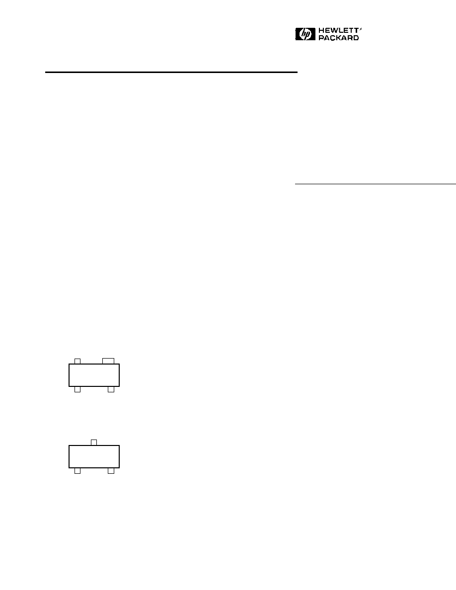
AT-41511
AT-41533
1. Refer to "Tape-and-Reel Packaging for
Semiconductor Devices."
BASE
EMITTER
EMITTER COLLECTOR
BASE
EMITTER
COLLECTOR
415
415
SOT 23 (AT-41533)
SOT 143 (AT-41511)
Outline Drawing
5965-8929E

4-135
Characterization Information, T
A
= 25
∞
C
AT-41511 AT-41533
Symbol
Parameters and Test Conditions
Units
Min Typ Min
Typ
NF
Noise Figure
f = 0.9 GHz
dB
1.0
1.0
V
CE
= 5 V, I
C
= 5 mA
f = 2.4 GHz
1.7
1.6
G
A
Associated Gain
f = 0.9 GHz
dB
15.5
14.5
V
CE
= 5 V, I
C
= 5 mA
f = 2.4 GHz
11
9
P
1dB
Power at 1 dB Gain Compression (opt tuning)
f = 0.9 GHz
dBm
14.5
14.5
V
CE
= 5 V, I
C
= 25 mA
G
1dB
Gain at 1 dB Gain Compression (opt tuning)
f = 0.9 GHz
dB
17.5
14.5
V
CE
= 5 V, I
C
= 25 mA
IP
3
Output Third Order Intercept Point,
f = 0.9 GHz
dBm
25
25
V
CE
= 5 V, I
C
=25 mA (opt tuning)
|S
21E
|
2
Gain in 50
system; V
CE
= 5 V, I
C
= 5 mA
f = 0.9 GHz
dB
13.5
15.5
10.8
12.8
f = 2.4 GHz
7.9
5.2
AT-41511, AT-41533 Absolute Maximum Ratings
Absolute
Symbol
Parameter
Units
Maximum
[1]
V
EBO
Emitter-Base Voltage
V
1.5
V
CBO
Collector-Base Voltage
V
20
V
CEO
Collector-Emitter Voltage
V
12
I
C
Collector Current
mA
50
P
T
Power Dissipation
[2,3]
mW
225
T
j
Junction Temperature
∞
C
150
T
STG
Storage Temperature
∞
C
-65 to 150
Electrical Specifications, T
A
= 25
∞
C
AT-41511
AT-41533
Symbol
Parameters and Test Conditions
Units Min
Typ
Max
Min
Typ
Max
h
FE
Forward Current Transfer Ratio
V
CE
= 5 V
-
30
150
270
30
150
270
I
C
= 5 mA
I
CBO
Collector Cutoff Current
V
CB
= 3 V
µ
A
0.2
0.2
I
EBO
Emitter Cutoff Current
V
EB
= 1 V
µ
A
1.0
1.0
Notes:
1. Operation of this device above any one
of these parameters may cause
permanent damage.
2. T
Mounting Surface
= 25
∞
C.
3. Derate at 1.82 mW/
∞
C for T
C
> 26
∞
C.
Thermal Resistance:
[2]
jc
=550
∞
C/W
Ordering Information
Part Number
Increment
Comments
AT-41511-BLK
100
Bulk
AT-41511-TR1
3000
7" Reel
AT-41533-BLK
100
Bulk
AT-41533-TR1
3000
7" Reel

4-136
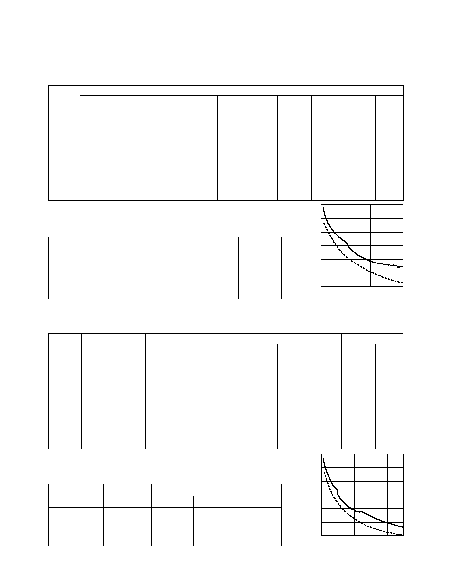
Figure 9. AT-41511 and AT-41533
P
1dB
vs. Frequency and Bias at
V
CE
= 8 V, with Optimal Tuning.
Figure 8. AT-41511 and AT-41533
P
1dB
vs. Frequency and Bias at
V
CE
= 5 V, with Optimal Tuning.
Figure 7. AT-41511 and AT-41533
P
1dB
vs. Frequency and Bias at
V
CE
= 2.7 V, with Optimal Tuning.
P
1 dB
(dBm)
0.1
20
0
FREQUENCY (GHz)
0.6
2.1
2.6
15
10
5
1.6
1.1
25 mA
10 mA
5 mA
P
1 dB
(dBm)
0.1
20
0
FREQUENCY (GHz)
0.6
2.1
2.6
15
10
5
1.6
1.1
25 mA
10 mA
5 mA
P
1 dB
(dBm)
0.1
20
0
FREQUENCY (GHz)
0.6
2.1
2.6
15
10
5
1.6
1.1
25 mA
10 mA
5 mA
AT-41511, AT-41533 Typical Performance
Figure 2. AT-41511 and AT-41533
Minimum Noise Figure vs. Frequency
and Current at V
CE
= 5 V.
Figure 1. AT-41511 and AT-41533
Minimum Noise Figure vs. Frequency
and Current at V
CE
= 2.7 V.
Figure 3. AT-41511 and AT-41533
Minimum Noise Figure vs. Frequency
and Current at V
CE
= 8 V.
NOISE FIGURE (dB)
0.1
3.0
0
FREQUENCY (GHz)
0.6
2.1
2.6
2.5
1.5
0.5
1.6
2.0
1.0
1.1
25 mA
10 mA
2, 5 mA
NOISE FIGURE (dB)
0.1
3.0
0
FREQUENCY (GHz)
0.6
2.1
2.6
2.5
1.5
0.5
1.6
2.0
1.0
1.1
25 mA
10 mA
5 mA
NOISE FIGURE (dB)
0.1
3.0
0
FREQUENCY (GHz)
0.6
2.1
2.6
2.5
1.5
0.5
1.6
2.0
1.0
1.1
25 mA
2 mA
10 mA
5 mA
G
a
PKG 11 (dB)
0.1
20
0
FREQUENCY (GHz)
0.6
2.1
2.6
15
10
5
1.6
1.1
20
15
10
G
a
PKG 33 (dB)
PKG 11
PKG 33
25
5
10, 25 mA
2 mA
5 mA
2 mA
5 mA
10, 25 mA
Figure 6. AT-41511 and AT-41533
Associated Gain vs. Frequency and
Current at V
CE
= 8 V.
Figure 5. AT-41511 and AT-41533
Associated Gain vs. Frequency and
Current at V
CE
= 5 V.
Figure 4. AT-41511 and AT-41533
Associated Gain vs. Frequency and
Current at V
CE
= 2.7 V.
G
a
(dB)
0.1
20
0
FREQUENCY (GHz)
0.6
2.1
2.6
15
10
5
1.6
1.1
PKG 11
PKG 33
10, 25 mA
5 mA
10, 25 mA
5 mA
G
a
(dB)
0.1
20
0
FREQUENCY (GHz)
0.6
2.1
2.6
15
10
5
1.6
1.1
PKG 11
PKG 33
10, 25 mA
5 mA
10, 25 mA
5 mA
4-137
AT-41511 Typical Scattering Parameters, Common Emitter, Z
o
= 50
, V
CE
= 2.7 V, I
C
= 5 mA
Freq.
S
11
S
21
S
12
S
22
GHz
Mag
Ang
dB
Mag
Ang
dB
Mag
Ang
Mag
Ang
0.1
0.84
-27
23.44
14.854
161
-34.89
0.018
76
0.95
-11
0.5
0.59
-102
19.01
8.924
115
-24.88
0.057
48
0.65
-34
0.9
0.49
-141
15.09
5.684
93
-22.97
0.071
43
0.51
-39
1.0
0.48
-149
14.30
5.189
89
-22.73
0.073
43
0.49
-39
1.5
0.46
-176
11.15
3.61
72
-21.21
0.087
44
0.44
-43
1.8
0.46
170
9.69
3.051
64
-20.26
0.097
45
0.43
-45
2.0
0.46
162
8.86
2.774
59
-19.74
0.103
45
0.42
-47
2.4
0.47
148
7.37
2.337
50
-18.64
0.117
46
0.42
-51
3.0
0.5
130
5.58
1.901
36
-17.14
0.139
45
0.41
-59
4.0
0.56
106
3.25
1.454
17
-14.89
0.18
42
0.4
-73
5.0
0.61
87
1.36
1.17
0
-12.96
0.225
37
0.4
-91
AT-41511 Typical Noise Parameters,
Common Emitter, Z
o
= 50
,
V
CE
=
2.7 V, I
C
= 5 mA
Freq
F
min
opt
R
n
GHz
dB
Mag
Ang
-
0.1
0.8
0.45
6
0.25
0.9
1.0
0.39
63
0.19
1.8
1.4
0.32
137
0.12
2.4
1.7
0.40
177
0.09
GAIN (dB)
0
30
0
FREQUENCY (GHz)
1
4
5
25
15
5
3
20
10
2
MSG
MAG
MSG
S21
Figure 10. AT-41511 Gains vs.
Frequency at V
CE
= 2.7 V, I
C
= 5 mA.
Figure 11. AT-41533 Gains vs.
Frequency at V
CE
= 2.7 V, I
C
= 5 mA.
GAIN (dB)
0
30
0
FREQUENCY (GHz)
1
4
5
25
15
5
3
20
10
2
MSG
MAG
MSG
S21
AT-41533 Typical Scattering Parameters, Common Emitter, Z
o
= 50
, V
CE
= 2.7 V, I
C
= 5 mA
Freq.
S
11
S
21
S
12
S
22
GHz
Mag
Ang
dB
Mag
Ang
dB
Mag
Ang
Mag
Ang
0.1
0.78
-30
23.43
14.834
155
-33.98
0.020
75
0.94
-12
0.5
0.35
-99
16.91
7.004
103
-24.58
0.059
60
0.62
-28
0.9
0.23
-144
12.50
4.219
84
-21.21
0.087
62
0.55
-30
1.0
0.21
-154
11.65
3.826
80
-20.54
0.094
63
0.54
-31
1.5
0.20
162
8.50
2.661
64
-17.46
0.134
64
0.52
-36
1.8
0.22
144
7.09
2.261
56
-15.97
0.159
63
0.51
-40
2.0
0.23
134
6.30
2.065
51
-15.09
0.176
63
0.51
-42
2.4
0.26
118
4.97
1.773
42
-13.39
0.214
61
0.50
-48
3.0
0.30
101
3.45
1.488
30
-11.21
0.275
56
0.48
-58
4.0
0.37
80
1.66
1.211
13
-8.20
0.389
46
0.45
-80
5.0
0.44
62
0.35
1.041
-1
-5.90
0.507
33
0.42
-104
AT-41533 Typical Noise Parameters,
Common Emitter, Z
o
= 50
,
V
CE
=
2.7 V, I
C
= 5 mA
Freq
F
min
opt
R
n
GHz
dB
Mag
Ang
-
0.1
0.7
0.45
8
0.20
0.9
1.0
0.25
94
0.13
1.8
1.4
0.38
-159
0.08
2.4
1.6
0.54
-122
0.16
4-138
AT-41511 Typical Scattering Parameters, Common Emitter, Z
o
= 50
, V
CE
= 2.7 V, I
C
= 25 mA
Freq.
S
11
S
21
S
12
S
22
GHz
Mag
Ang
dB
Mag
Ang
dB
Mag
Ang
Mag
Ang
0.1
0.49
-91
29.26
29.048
136
-37.72
0.013
62
0.73
-22
0.5
0.53
-168
18.55
8.459
92
-30.46
0.030
61
0.45
-23
0.9
0.53
172
13.62
4.798
79
-26.56
0.047
66
0.42
-26
1.0
0.53
169
12.73
4.330
76
-25.68
0.052
67
0.42
-27
1.5
0.54
153
9.34
2.932
63
-22.50
0.075
67
0.42
-34
1.8
0.55
145
7.86
2.473
57
-21.01
0.089
66
0.42
-38
2.0
0.56
140
6.97
2.232
52
-20.09
0.099
66
0.42
-41
2.4
0.57
129
5.47
1.877
44
-18.49
0.119
64
0.42
-48
3.0
0.60
116
3.67
1.525
32
-16.54
0.149
59
0.41
-58
4.0
0.64
95
1.30
1.162
14
-13.98
0.200
51
0.40
-75
5.0
0.67
79
-0.58
0.935
-1
-11.90
0.254
43
0.39
-96
AT-41511 Typical Noise Parameters,
Common Emitter, Z
o
= 50
,
V
CE
=
2.7 V, I
C
= 25 mA
Freq
F
min
opt
R
n
GHz
dB
Mag
Ang
-
0.1
1.6
0.13
18
0.16
0.9
1.9
0.24
-162
0.13
1.8
2.3
0.40
-137
0.23
2.4
2.7
0.50
-122
0.35
GAIN (dB)
0
30
0
FREQUENCY (GHz)
1
4
5
25
15
5
3
20
10
2
MSG
MAG
MSG
S21
Figure 12. AT-41511 Gains vs.
Frequency at V
CE
= 2.7 V, I
C
= 25 mA.
AT-41533 Typical Scattering Parameters,
Common Emitter, Z
o
= 50
, V
CE
= 2.7 V, I
C
= 25 mA
Freq.
S
11
S
21
S
12
S
22
GHz
Mag
Ang
dB
Mag
Ang
dB
Mag
Ang
Mag
Ang
0.1
0.34
-75
29.37
29.404
127
-37.08
0.014
72
0.71
-21
0.5
0.19
-168
17.63
7.614
88
-25.68
0.052
76
0.47
-20
0.9
0.20
161
12.73
4.329
74
-20.82
0.091
74
0.46
-24
1.0
0.20
154
11.84
3.909
71
-19.91
0.101
74
0.45
-26
1.5
0.24
132
8.56
2.679
59
-16.42
0.151
70
0.45
-33
1.8
0.25
121
7.12
2.271
52
-14.85
0.181
67
0.44
-38
2.0
0.27
115
6.32
2.071
47
-13.94
0.201
65
0.44
-41
2.4
0.29
105
4.99
1.777
39
-12.32
0.242
61
0.43
-48
3.0
0.33
93
3.46
1.489
27
-10.31
0.305
54
0.41
-59
4.0
0.39
76
1.69
1.215
11
-7.66
0.414
42
0.37
-81
5.0
0.45
60
0.40
1.047
-3
-5.73
0.517
29
0.33
-106
AT-41533 Typical Noise Parameters,
Common Emitter, Z
o
= 50
,
V
CE
=
2.7 V, I
C
= 25 mA
Freq
F
min
opt
R
n
GHz
dB
Mag
Ang
-
0.1
1.3
0.10
24
0.12
0.9
1.6
0.25
-158
0.11
1.8
1.9
0.48
-122
0.19
2.4
2.1
0.59
-101
0.37
GAIN (dB)
0
30
0
FREQUENCY (GHz)
1
4
5
25
15
5
3
20
10
2
MSG
MAG
MSG
S21
Figure 13. AT-41533 Gains vs.
Frequency at V
CE
= 2.7 V, I
C
= 25 mA.