 | –≠–ª–µ–∫—Ç—Ä–æ–Ω–Ω—ã–π –∫–æ–º–ø–æ–Ω–µ–Ω—Ç: AT42085 | –°–∫–∞—á–∞—Ç—å:  PDF PDF  ZIP ZIP |
Document Outline
- List of Figures
- 1. Insertion Power Gain vs. Collector Current and Frequency. V CE = 8 V.
- 2. Output Power and 1 dB Compressed Gain vs. Collector Current and Frequency. V CE = 8 V.
- 3. Output Power and 1 dB Compressed Gain vs. Collector Current and Voltage. f = 2.0 GHz.
- 4. Insertion Power Gain, Maximum Available Gain and Maximum Stable Gain vs. Frequency. V CE = 8 V, I C = 35 mA.
- 5. Noise Figure and Associated Gain vs. Frequency. V CE = 8 V, I C = 10mA.
- Features
- Description
- 85 Plastic Package
- AT-42085 Absolute Maximum Ratings
- Electrical Specifications, TA = 25∞C
- AT-42085 Typical Performance, TA = 25∞C
- AT-42085 Typical Scattering Parameters,
- AT-42085 Typical Scattering Parameters,
- AT-42085 Noise Parameters: VCE = 8 V, IC = 10 mA
- 85 Plastic Package Dimensions

4-169
Up to 6 GHz Medium Power
Silicon Bipolar Transistor
Technical Data
Features
∑ High Output Power:
20.5 dBm Typical P
1 dB
at 2.0 GHz
∑ High Gain at 1 dB
Compression:
14.0 dB Typical G
1 dB
at 2.0 GHz
∑ Low Noise Figure:
2.0 dB Typical NF
O
at 2.0 GHz
∑ High Gain-Bandwidth
Product: 8.0 GHz Typical f
T
∑ Low Cost Plastic Package
AT-42085
85 Plastic Package
Description
Hewlett-Packard's AT-42085 is a
general purpose NPN bipolar
transistor that offers excellent
high frequency performance. The
AT-42085 is housed in a low cost
.085" diameter plastic package.
The 4 micron emitter-to-emitter
pitch enables this transistor to be
used in many different functions.
The 20 emitter finger interdigi-
tated geometry yields a medium
sized transistor with impedances
that are easy to match for low
noise and medium power applica-
tions. Applications include use in
wireless systems as an LNA, gain
stage, buffer, oscillator, and
mixer. An optimum noise match
near 50
up to 1 GHz, makes this
device easy to use as a low noise
amplifier.
The AT-42085 bipolar transistor is
fabricated using Hewlett-Packard's
10 GHz f
T
Self-Aligned-Transistor
(SAT) process. The die is nitride
passivated for surface protection.
Excellent device uniformity,
performance and reliability are
produced by the use of ion-
implantation, self-alignment
techniques, and gold metalization
in the fabrication of this device.
5965-8913E
4-170
AT-42085 Absolute Maximum Ratings
Absolute
Symbol
Parameter
Units
Maximum
[1]
V
EBO
Emitter-Base Voltage
V
1.5
V
CBO
Collector-Base Voltage
V
20
V
CEO
Collector-Emitter Voltage
V
12
I
C
Collector Current
mA
80
P
T
Power Dissipation
[2,3]
mW
500
T
j
Junction Temperature
∞
C
150
T
STG
Storage Temperature
∞
C
-65 to 150
Thermal Resistance
[2,4]
:
jc
= 130
∞
C/W
Notes:
1. Permanent damage may occur if
any of these limits are exceeded.
2. T
CASE
= 25
∞
C.
3. Derate at 7.7 mW/
∞
C for T
C
> 85
∞
C.
4. See MEASUREMENTS section
"Thermal Resistance" for more
information.
|S
21E
|
2
Insertion Power Gain; V
CE
= 8 V, I
C
= 35 mA
f = 1.0 GHz
dB
15.5
17.0
f = 2.0 GHz
11.0
f = 4.0 GHz
5.0
P
1 dB
Power Output @ 1 dB Gain Compression
f = 2.0 GHz
dBm
20.5
V
CE
= 8 V, I
C
= 35 mA
f= 4.0 GHz
20.0
G
1 dB
1 dB Compressed Gain; V
CE
= 8 V, I
C
= 35 mA
f = 2.0 GHz
dB
14.0
f = 4.0 GHz
9.5
NF
O
Optimum Noise Figure: V
CE
= 8 V, I
C
= 10 mA
f = 2.0 GHz
dB
2.0
f = 4.0 GHz
3.5
G
A
Gain @ NF
O
; V
CE
= 8 V, I
C
= 10 mA
f = 2.0 GHz
dB
13.5
f = 4.0 GHz
9.5
f
T
Gain Bandwidth Product: V
CE
= 8 V, I
C
= 35 mA
GHz
8.0
h
FE
Forward Current Transfer Ratio; V
CE
= 8 V, I
C
= 35 mA
--
30
150
270
I
CBO
Collector Cutoff Current; V
CB
= 8 V
µ
A
0.2
I
EBO
Emitter Cutoff Current; V
EB
= 1 V
µ
A
2.0
C
CB
Collector Base Capacitance
[1]
: V
CB
= 8 V, f = 1 MHz
pF
0.32
Note:
1. For this test, the emitter is grounded.
Electrical Specifications, T
A
= 25
∞
C
Symbol
Parameters and Test Conditions
Units Min.
Typ. Max.
4-171
AT-42085 Typical Performance, T
A
= 25
∞
C
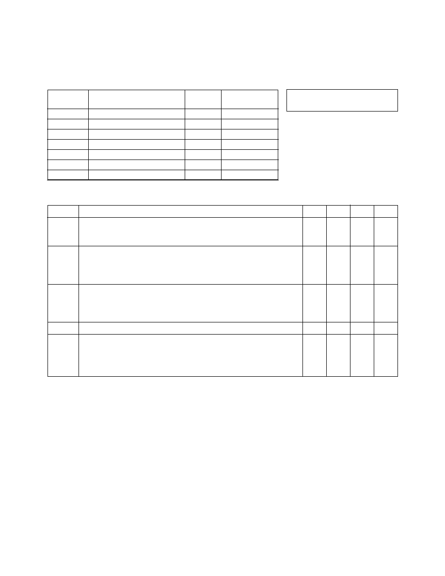
FREQUENCY (GHz)
Figure 4. Insertion Power Gain,
Maximum Available Gain and
Maximum Stable Gain vs. Frequency.
V
CE
= 8 V, I
C
= 35 mA.
GAIN (dB)
0.1
0.5
0.3
1.0
3.0
6.0
I
C
(mA)
Figure 2. Output Power and 1 dB
Compressed Gain vs. Collector
Current and Frequency. V
CE
= 8 V.
24
20
16
12
8
4
G
1 dB
(dB)
P
1 dB
(dBm)
0
10
20
30
40
50
P1dB
G1dB
2.0 GHz
2.0 GHz
4.0 GHz
4.0 GHz
40
35
30
25
20
15
10
5
0
MSG
MAG
|S21E|
2
I
C
(mA)
Figure 1. Insertion Power Gain vs.
Collector Current and Frequency.
V
CE
= 8 V.
20
16
12
8
4
0
|S
21E
|
2
GAIN (dB)
0
10
20
30
40
50
1.0 GHz
2.0 GHz
4.0 GHz
I
C
(mA)
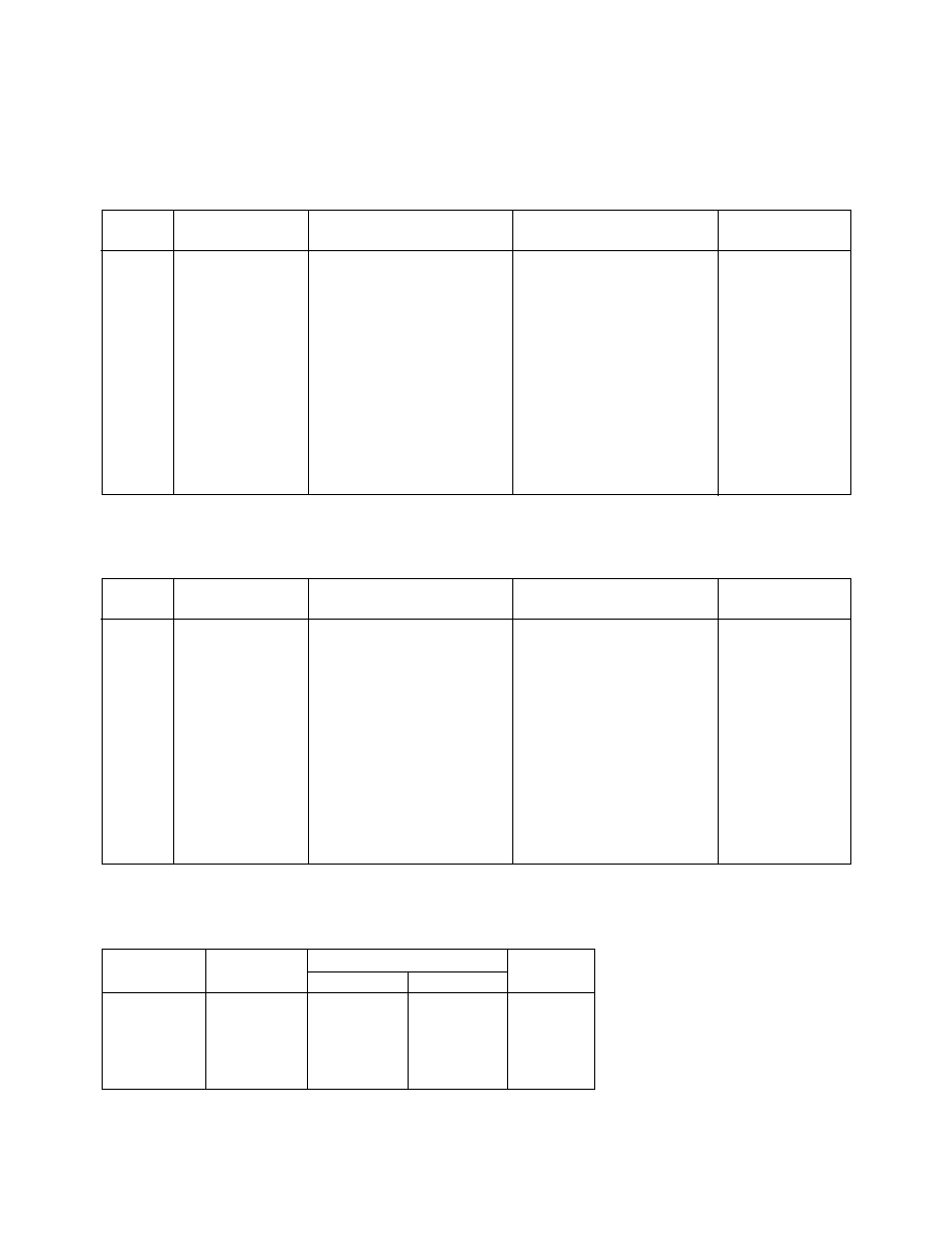
Figure 3. Output Power and 1 dB
Compressed Gain vs. Collector
Current and Voltage. f = 2.0 GHz.
10 V
4 V
6 V
4 V
10 V
6 V
24
20
16
12
16
14
12
10
G
1 dB
(dB)
P
1 dB
(dBm)
0
10
20
30
40
50
P1dB
G1dB
FREQUENCY (GHz)
Figure 5. Noise Figure and Associated
Gain vs. Frequency.
V
CE
= 8 V, I
C
= 10mA.
GAIN (dB)
24
21
18
15
12
9
6
3
0
4
3
2
1
0
NF
O
(dB)
0.5
2.0
1.0
3.0
4.0 5.0
GA
NFO
4-172
AT-42085 Typical Scattering Parameters,
Common Emitter, Z
O
= 50
, T
A
= 25
∞
C, V
CE
= 8 V, I
C
= 10 mA
Freq.
S
11
S
21
S
12
S
22
GHz
Mag.
Ang.
dB
Mag.
Ang.
dB
Mag.
Ang.
Mag.
Ang.
0.1
.72
-50
28.5
26.52
152
-37.0
.014
73
.90
-16
0.5
.66
-139
21.0
11.23
103
-29.2
.035
36
.53
-32
1.0
.65
-168
15.5
5.96
84
-28.6
.037
39
.45
-33
1.5
.65
175
12.2
4.06
71
-27.0
.045
46
.43
-36
2.0
.65
163
9.7
3.06
60
-25.3
.054
51
.42
-41
2.5
.66
157
8.0
2.51
55
-24.0
.063
60
.42
-42
3.0
.68
149
6.3
2.07
46
-22.8
.072
65
.41
-48
3.5
.68
141
5.1
1.79
38
-21.4
.085
64
.43
-55
4.0
.69
133
3.9
1.57
29
-19.7
.104
64
.45
-61
4.5
.69
125
3.0
1.41
21
-18.5
.119
63
.46
-66
5.0
.69
114
2.2
1.28
12
-17.1
.139
58
.47
-71
5.5
.71
103
1.4
1.17
3
-15.9
.161
55
.44
-76
6.0
.75
91
0.6
1.07
-6
-15.1
.177
49
.40
-85
AT-42085 Typical Scattering Parameters,
Common Emitter, Z
O
= 50
, T
A
= 25
∞
C, V
CE
= 8 V, I
C
= 35 mA
Freq.
S
11
S
21
S
12
S
22
GHz
Mag.
Ang.
dB
Mag.
Ang.
dB
Mag.
Ang.
Mag.
Ang.
0.1
.54
-90
33.1
45.38
137
-40.1
.010
66
.76
-26
0.5
.61
-163
22.6
13.45
95
-32.8
.023
52
.38
-30
1.0
.61
178
16.8
6.90
79
-29.5
.034
61
.34
-28
1.5
.62
167
13.4
4.67
68
-26.4
.048
68
.32
-31
2.0
.63
156
10.9
3.52
59
-23.9
.064
66
.31
-36
2.5
.64
152
9.2
2.89
54
-22.5
.075
68
.31
-40
3.0
.66
146
7.6
2.39
45
-21.2
.088
69
.30
-48
3.5
.67
139
6.3
2.07
37
-19.8
.102
67
.31
-58
4.0
.68
131
5.2
1.81
28
-18.6
.117
65
.33
-67
4.5
.68
123
4.2
1.62
19
-17.2
.138
60
.35
-73
5.0
.68
114
3.4
1.48
10
-16.4
.152
56
.35
-79
5.5
.71
103
2.5
1.34
1
-15.3
.171
50
.34
-85
6.0
.74
93
1.7
1.21
-8
-14.5
.188
46
.31
-96
A model for this device is available in the DEVICE MODELS section.
AT-42085 Noise Parameters:
V
CE
= 8 V, I
C
= 10 mA
Freq.
NF
O
opt
GHz
dB
Mag
Ang
R
N
/50
0.1
1.1
.05
16
0.13
0.5
1.2
.06
77
0.13
1.0
1.3
.10
131
0.12
2.0
2.0
.24
-179
0.11
4.0
3.5
.46
-128
0.25
4-173
85 Plastic Package Dimensions
1
3
4
2
5
∞
TYP.
45
∞
EMITTER
EMITTER
COLLECTOR
BASE
.085
2.15
.286
±
.030
7.36
±
.76
Notes:
(unless otherwise specified)
1. Dimensions are in
2. Tolerances
in .xxx =
±
0.005
mm .xx =
±
0.13
mm
.020
.51
.07
0.43
.060
±
.010
1.52
±
.25
.006
±
.002
.15
±
.05
0.143
±
0.015
3.63
±
0.38
420