 | –≠–ª–µ–∫—Ç—Ä–æ–Ω–Ω—ã–π –∫–æ–º–ø–æ–Ω–µ–Ω—Ç: ATF33143 | –°–∫–∞—á–∞—Ç—å:  PDF PDF  ZIP ZIP |
1
Low Noise Pseudomorphic HEMT
in a Surface Mount Plastic Package
Technical Data
ATF-33143
Features
∑ Low Noise Figure
∑ Excellent Uniformity in
Product Specifications
∑ Low Cost Surface Mount
Small Plastic Package
SOT-343 (4 lead SC-70)
∑ Tape-and-Reel Packaging
Option Available
Specifications
1.9 GHz; 4 V, 80 mA (Typ.)
∑ 0.5 dB Noise Figure
∑ 15 dB Associated Gain
∑ 22 dBm Output Power at
1 dB Gain Compression
∑ 33.5 dBm Output 3
rd
Order
Intercept
Applications
∑ Low Noise Amplifier and
Driver Amplifier for
Cellular/PCS Base Stations
∑ LNA for WLAN, WLL/RLL,
LEO, and MMDS
Applications
∑ General Purpose Discrete
PHEMT for Other Ultra Low
Noise Applications
Surface Mount Package
SOT-343
Description
Agilent's ATF-33143 is a high
dynamic range, low noise,
PHEMT housed in a 4-lead SC-70
(SOT-343) surface mount plastic
package.
Based on its featured perfor-
mance, ATF-33143 is suitable for
applications in cellular and PCS
base stations, LEO systems,
MMDS, and other systems requir-
ing super low noise figure with
good intercept in the 450 MHz to
10 GHz frequency range.
Pin Connections and
Package Marking
GATE
3Px
SOURCE
DRAIN
SOURCE
Note:
Top View. Package marking
provides orientation and identification.
"3P" = Device code
"x" = Date code character. A new
character is assigned for each month, year.
88759/05-2.PM6.5J
2001.04.26, 9:12 AM
Page 1
Adobe PageMaker 6.5J/PPC
2
ATF-33143 Absolute Maximum Ratings
[1]
Absolute
Symbol
Parameter
Units
Maximum
V
DS
Drain - Source Voltage
[2]
V
5.5
V
GS
Gate - Source Voltage
[2]
V
-5
V
GD
Gate Drain Voltage
[2]
V
-5
I
DS
Drain Current
[2]
mA
I
dss
[3]
P
diss
Total Power Dissipation
[4]
mW
600
P
in max
RF Input Power
dBm
20
T
CH
Channel Temperature
[5]
∞
C
160
T
STG
Storage Temperature
∞
C
-65 to 160
jc
Thermal Resistance
[6]
∞
C/W
145
Notes:
1. Operation of this device above any one
of these parameters may cause
permanent damage.
2. Assumes DC quiesent conditions.
3. V
GS
= 0 V
4. Source lead temperature is 25
∞
C.
Derate 6 mW/
∞
C for T
L
> 60
∞
C.
5. Please refer to failure rates in reliability
section to assess the reliability impact
of running devices above a channel
temperature of 140
∞
C.
6. Thermal resistance measured using
150
∞
C Liquid Crystal Measurement
method.
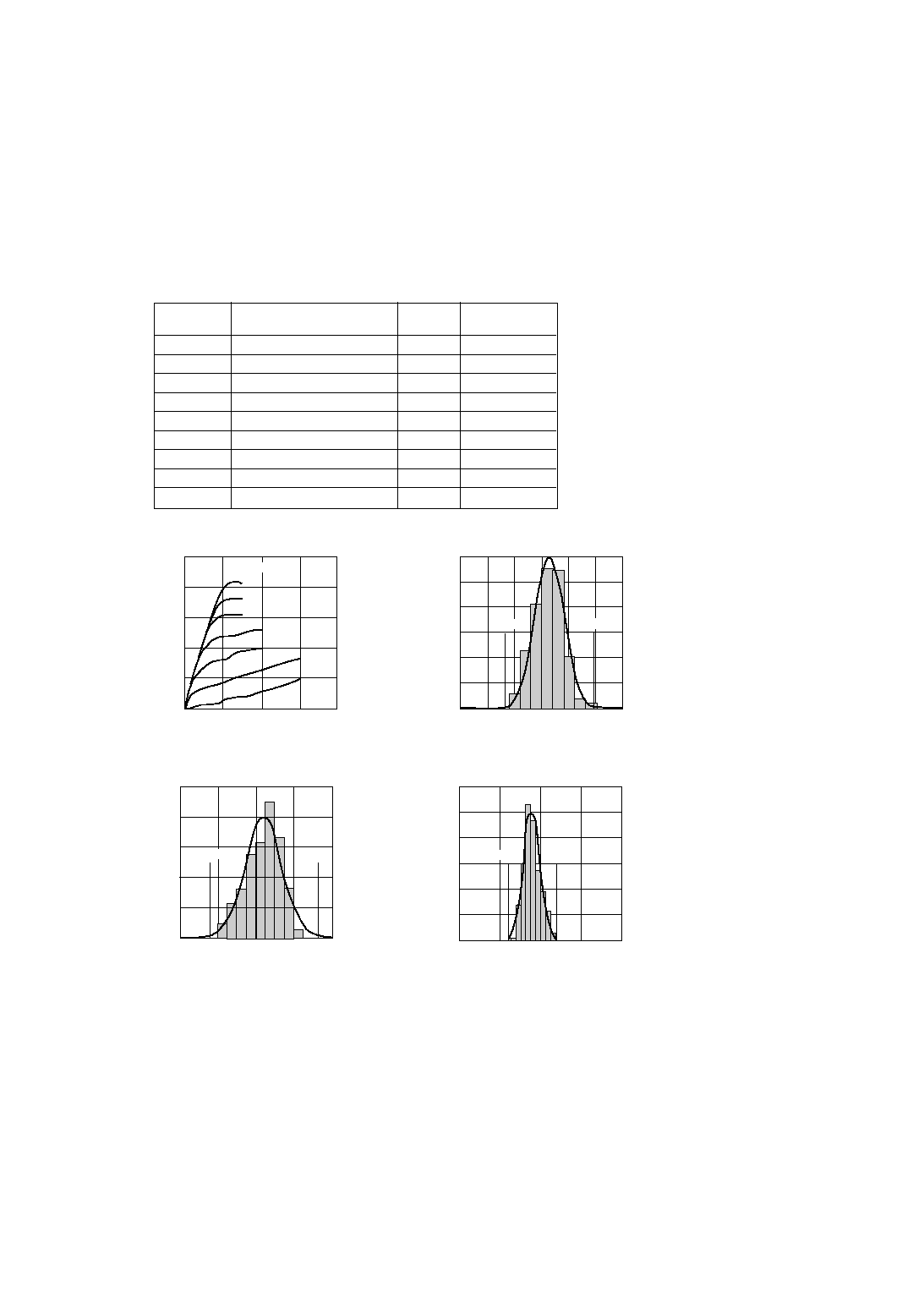
Product Consistency Distribution Charts
[8, 9]
V
DS
(V)
Figure 1. Typical Pulsed I-V Curves
[7]
.
(V
GS
= -0.2 V per step)
I
DS
(mA)
0
2
4
6
8
500
400
300
200
100
0
0 V
≠0.6 V
+0.6 V
NF (dB)
Figure 2. NF @ 2 GHz, 4 V, 80 mA.
LSL=0.2, Nominal=0.53, USL=0.8
0.2
0.4
0.3
0.6
0.5
0.8
0.7
-3 Std
+3 Std
Cpk = 1.7
Std = 0.05
120
100
80
60
40
20
0
OIP3 (dBm)
Figure 3. OIP3 @ 2 GHz, 4 V, 80 mA.
LSL=30.0, Nominal=33.3, USL=37.0
29
37
-3 Std
+3 Std
Cpk = 1.21
Std = 0.94
100
80
60
40
20
0
33
31
35
GAIN (dB)
Figure 4. Gain @ 2 GHz, 4 V, 80 mA.
LSL=13.5, Nominal=14.8, USL=16.5
13
14
15
16
17
-3 Std
+3 Std
Cpk = 2.3
Std = 0.2
120
100
80
60
40
20
0
Notes:
7. Under large signal conditions, V
GS
may
swing positive and the drain current may
exceed I
dss
. These conditions are
acceptable as long as the maximum P
diss
and P
in max
ratings are not exceeded.
8. Distribution data sample size is 450
samples taken from 9 different wafers.
Future wafers allocated to this product
may have nominal values anywhere
within the upper and lower spec limits.
9. Measurements made on production test
board. This circuit represents a trade-off
between an optimal noise match and a
realizeable match based on production
test requirements. Circuit losses have
been de-embedded from actual
measurements.
10. The probability of a parameter being
between
±
1
is 68.3%, between
±
2
is
95.4% and between
±
3
is 99.7%.
88759/05-2.PM6.5J
2001.04.26, 9:12 AM
Page 2
Adobe PageMaker 6.5J/PPC

3
Figure 5. Block diagram of 2 GHz production test board used for Noise Figure, Associated Gain, P
1dB
, and OIP3 measure-
ments. This circuit represents a trade-off between an optimal noise match and a realizable match based on production test
requirements. Circuit losses have been de-embedded from actual measurements.
Input
50 Ohm
Transmission
Line Including
Gate Bias T
(0.5 dB loss)
Input
Matching Circuit
_mag = 0.20
_ang = 124
∞
(0.3 dB loss)
DUT
50 Ohm
Transmission
Line Including
Drain Bias T
(0.5 dB loss)
Output
ATF-33143 DC Electrical Specifications
T
A
= 25
∞
C, RF parameters measured in a test circuit for a typical device
Symbol
Parameters and Test Conditions
Units Min. Typ.
[2]
Max.
I
dss
[1]
Saturated Drain Current
V
DS
= 1.5 V, V
GS
= 0 V
mA
175
237
305
V
P
[1]
Pinchoff Voltage
V
DS
= 1.5 V, I
DS
= 10% of I
dss
V
-0.65
-0.5
- 0.35
I
d
Quiescent Bias Current
V
GS
= -0.5 V, V
DS
= 4 V
mA
--
80
--
g
m
[1]
Transconductance
V
DS
= 1.5 V, g
m
= I
dss
/V
P
mmho 360
440
--
I
GDO
Gate to Drain Leakage Current
V
GD
= 5 V
µ
A
1000
I
gss
Gate Leakage Current
V
GD
= V
GS
= -4 V
µ
A
--
42
600
f = 2 GHz
V
DS
= 4 V, I
DS
= 80 mA
dB
0.5
0.8
NF
Noise Figure
V
DS
= 4 V, I
DS
= 60 mA
0.5
f = 900 MHz
V
DS
= 4 V, I
DS
= 80 mA
dB
0.4
V
DS
= 4 V, I
DS
= 60 mA
0.4
f = 2 GHz
V
DS
= 4 V, I
DS
= 80 mA
dB
13.5
15
16.5
G
a
Associated Gain
[3]
V
DS
= 4 V, I
DS
= 60 mA
15
f = 900 MHz
V
DS
= 4 V, I
DS
= 80 mA
dB
21
V
DS
= 4 V, I
DS
= 60 mA
21
Output 3
rd
Order
f = 2 GHz
V
DS
= 4 V, I
DS
= 80 mA
dBm
30
33.5
OIP3
Intercept Point
[3]
5 dBm Pout/Tone
V
DS
= 4 V, I
DS
= 60 mA
32
f = 900 MHz
V
DS
= 4 V, I
DS
= 80 mA
dBm
32.5
5 dBm Pout/Tone
V
DS
= 4 V, I
DS
= 60 mA
31
1 dB Compressed
f = 2 GHz
V
DS
= 4 V, I
DS
= 80 mA
dBm
22
P
1dB
Compressed Power
[3]
V
DS
= 4 V, I
DS
= 60 mA
21
f = 900 MHz
V
DS
= 4 V, I
DS
= 80 mA
dBm
21
V
DS
= 4 V, I
DS
= 60 mA
20
Notes:
1. Guaranteed at wafer probe level.
2. Typical value determined from a sample size of 450 parts from 9 wafers.
3. Measurements obtained using production test board described in Figure 5.
88759/05-2.PM6.5J
2001.04.26, 9:12 AM
Page 3
Adobe PageMaker 6.5J/PPC
4
ATF-33143 Typical Performance Curves
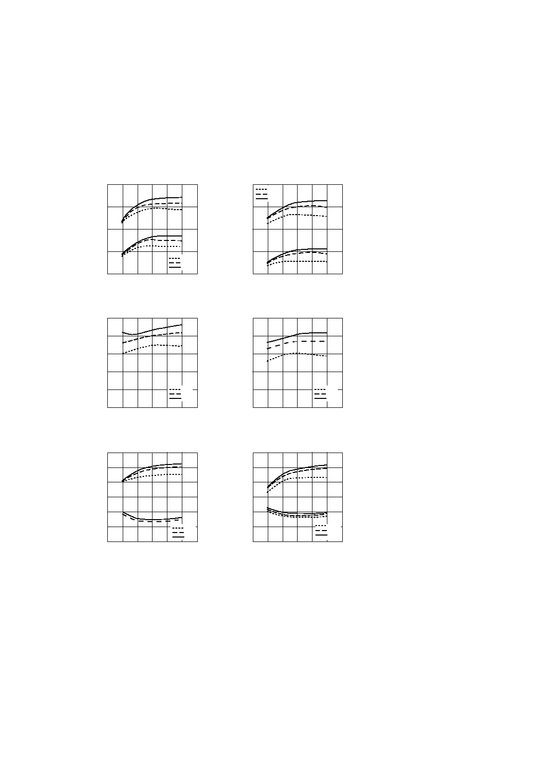
Notes:
1. Measurements made on a fixed tuned production test board that was tuned for optimal gain match with reasonable noise figure at 4V
80 mA bias. This circuit represents a trade-off between optimal noise match, maximum gain match and a realizable match based on
production test board requirements. Circuit losses have been de-embedded from actual measurements.
2. Quiescent drain current, I
DSQ
, is set with zero RF drive applied. As P
1dB
is approached, the drain current may increase or decrease
depending on frequency and dc bias point. At lower values of I
DSQ
the device is running closer to class B as power output approaches
P
1dB
. This results in higher P
1dB
and higher PAE (power added efficiency) when compared to a device that is driven by a constant
current source as is typically done with active biasing.
Figure 8. P
1dB
vs. Bias
[1,2]
at 2 GHz.
Figure 9. P
1dB
vs. Bias
[1,2]
Tuned for NF
@ 4V, 80mA at 900MHz.
Figure 10. NF and G
a
vs. Bias
[1]
at
2GHz.
Figure 11. NF and G
a
vs. Bias
[1]
at
900 MHz.
I
DSQ
(mA)
Figure 6. OIP3, IIP3 vs. Bias
[1]
at
2GHz.
OIP3,
IIP3 (dBm)
0
120
40
30
20
10
0
40
20
100
80
60
2 V
3 V
4 V
I
DSQ
(mA)
Figure 7. OIP3, IIP3 vs. Bias
[1]
at
900 MHz.
OIP3,
IIP3 (dBm)
40
30
20
10
0
2 V
3 V
4 V
0
120
40
20
100
80
60
I
DSQ
(mA)
P
1dB
(dBm)
25
20
15
10
5
0
2 V
3 V
4 V
0
120
40
20
80
100
60
NF
G
a
I
DSQ
(mA)
G
a
(dB)
16
15
14
13
12
11
10
1.4
1.2
1.0
0.8
0.6
0.4
0.2
NOISE FIGURE (dB)
2 V
3 V
4 V
0
120
40
20
80
100
60
I
DSQ
(mA)
G
a
(dB)
22
21
20
19
18
17
16
1.2
1.0
0.8
0.6
0.4
0.2
0
NOISE FIGURE (dB)
2 V
3 V
4 V
NF
G
a
0
120
40
20
80
100
60
I
DSQ
(mA)
P
1dB
(dBm)
25
20
15
10
5
0
2 V
3 V
4 V
0
120
40
20
80
100
60
88759/05-2.PM6.5J
2001.04.26, 9:12 AM
Page 4
Adobe PageMaker 6.5J/PPC
5
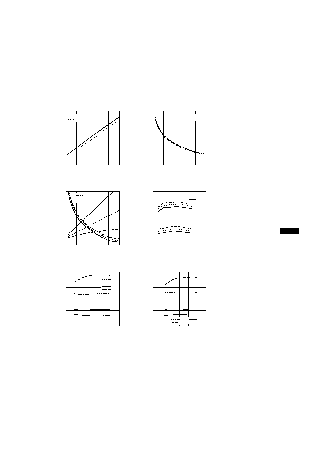
ATF-33143 Typical Performance Curves,
continued
Notes:
1. Measurements made on a fixed tuned test fixture that was tuned for noise figure at 4V 80 mA bias. This circuit represents a trade-off
between optimal noise match, maximum gain match and a realizable match based on production test requirements. Circuit losses have
been de-embedded from actual measurements.
2. Quiescent drain current, I
DSQ
, is set with zero RF drive applied. As P
1dB
is approached, the drain current may increase or decrease
depending on frequency and dc bias point. At lower values of I
dsq
the device is running closer to class B as power output approaches
P
1dB
. This results in higher P
1dB
and higher PAE (power added efficiency) when compared to a device that is driven by a constant
current source as is typically done with active biasing.
Figure 12. F
min
vs. Frequency and
Current at 4 V.
Figure 13. Associated Gain vs.
Frequency and Current at 4 V.
FREQUENCY (MHz)
Figure 15. P
1dB
, OIP3
vs. Frequency
and Temp at V
DS
= 4 V, I
DS
= 80mA.
P
1dB
,
OIP3 (dBm)
0
8000
40
35
30
25
20
15
4000
2000
6000
25
∞
C
-40
∞
C
85
∞
C
Figure 16. OIP3, P
1dB
, NF and Gain vs.
Bias
[1,2]
at 3.9 GHz.
Figure 17. OIP3, P
1dB
, NF and Gain vs.
Bias
[1,2]
at 5.8 GHz.
3.5
3.0
2.5
2.0
1.5
1.0
0.5
0
FREQUENCY (GHz)
F
min
(dB)
0
10
1.5
1.0
0.5
0
4
2
8
6
80 mA
60 mA
FREQUENCY (GHz)
G
a
(dB)
0
10
30
25
20
15
10
5
0
4
2
8
6
80 mA
60 mA
FREQUENCY (GHz)
G
a
(dB)
NOISE FIGURE (dB)
25
20
15
10
5
2.0
1.5
1.0
0.5
0
25
∞
C
-40
∞
C
85
∞
C
0
10
4
2
8
6
Figure 14. F
min
and G
a
vs. Frequency
and Temp at V
DS
= 4 V, I
DS
= 80mA.
I
DSQ
(mA)
OIP3,
P
1dB
(dBm),
GAIN (dB)
35
30
25
20
15
10
5
0
NOISE FIGURE (dB)
P
1dB
OIP3
Gain
NF
0
120
40
20
80
100
60
I
DSQ
(mA)
OIP3,
P
1dB
(dBm),
GAIN (dB)
35
30
25
20
15
10
5
0
NOISE FIGURE (dB)
3
2
1
0
P
1dB
OIP3
NF
Gain
0
120
40
20
80
100
60
88759/05-2.PM6.5J
2001.04.26, 9:12 AM
Page 5
Adobe PageMaker 6.5J/PPC