Document Outline
- ATF-331M4
- Features
- Specifications
- Applications
- Description
- MiniPak 1.4 mm x 1.2 mm Package
- Pin Connections and Package Marking
- Absolute Maximum Ratings
- Product Consistency Distribution Charts
- Electrical Specifications
- Typical Performance Curves
- Typical Scattering Parameters
- Typical Noise Parameters
- S and Noise Parameter Measurements
- Noise Parameter Applications Information
- SMT Assembly
- Electrostatic Sensitivity
- Die Model
- Minipak Model
- Ordering Information
- MiniPak Package Outline Drawing
- Solder Pad Dimensions
- Device Orientation
- Tape Dimensions

Agilent ATF-331M4 Low Noise
Pseudomorphic HEMT in a
Miniature Leadless Package
Data Sheet
Description
Agilent Technologies's
ATF-331M4 is a high linearity,
low noise pHEMT housed in a
miniature leadless package.
The ATF-331M4's small size and
low profile makes it ideal for the
design of hybrid modules and
other space-constraint devices.
Based on its featured perfor-
mance, ATF-331M4 is ideal for
the first or second stage of base
station LNA due to the excellent
combination of low noise figure
and enhanced linearity
[1]
. The
device is also suitable for appli-
cations in Wireless LAN,
WLL/RLL, MMDS, and other
systems requiring super low
noise figure with good intercept
in the 450 MHz to 10 GHz
frequency range.
Note:
1. From the same PHEMT FET family, the
smaller geometry ATF-34143 may also be
considered for the higher gain performance,
particularly in the higher frequency band
(1.8 GHz and up).
Features
� Low noise figure
� Excellent uniformity in product
specifications
� 1600 micron gate width
� Miniature leadless package
1.4 mm x 1.2 mm x 0.7 mm
� Tape-and-reel packaging option
available
Specifications
2 GHz; 4 V, 60 mA (Typ.)
� 0.6 dB noise figure
� 15 dB associated gain
� 19 dBm output power at 1 dB gain
compression
� 31 dBm output 3
rd
order intercept
Applications
� Tower mounted amplifier, low noise
amplifier and driver amplifier for
GSM/TDMA/CDMA base stations
� LNA for WLAN, WLL/RLL, MMDS
and wireless data infrastructures
�
General purpose discrete PHEMT for
other ultra low noise applications
MiniPak 1.4 mm x 1.2 mm Package
Pin Connections and
Package Marking
Note:
Top View. Package marking provides orientation,
product identification and date code.
"P" = Device Type Code
"x" = Date code character. A different
character is assigned for each month
and year.
Px
Source
Pin 3
Gate
Pin 2
Source
Pin 1
Drain
Pin 4
Px

2
ATF-331M4 Absolute Maximum Ratings
[1]
Absolute
Symbol
Parameter
Units
Maximum
V
DS
Drain-Source Voltage
[2]
V
5.5
V
GS
Gate-Source Voltage
[2]
V
-5
V
GD
Gate Drain Voltage
[2]
V
-5
I
DS
Drain Current
[2]
mA
I
diss
[3]
P
diss
Total Power Dissipation
[4]
mW
400
P
in max.
RF Input Power
dBm
20
T
CH
Channel Temperature
[5]
�
C
160
T
STG
Storage Temperature
�
C
-65 to 160
jc
Thermal Resistance
[6]
�
C/W
200
Notes:
1. Operation of this device above any one of
these parameters may cause permanent
damage.
2. Assumes DC quiescent conditions.
3. V
GS
= 0 V
4. Source lead temperature is 25
�
C. Derate
5 mW/
�
C for T
L
> 40
�
C.
5. Please refer to failure rates in reliability data
sheet to assess the reliability impact of
running devices above a channel temperature
of 140
�
C.
6. Thermal resistance measured using 150
�
C
Liquid Crystal Measurement method.
Product Consistency Distribution Charts
[8, 9]
V
DS
(V)
Figure 1. Typical Pulsed I-V Curves
[7]
.
(V
GS
= -0.2 V per step)
I
DS
(mA)
0
2
4
6
8
500
400
300
200
100
0
-0.6 V
0 V
+0.6 V
NF (dBm)
Figure 2. NF @ 2 GHz, 4 V, 60 mA.
LSL = 28.5, Nominal = 0.6, USL = 0.8.
0.2
0.4
0.5
0.6
0.7
0.3
0.8
0.9
100
80
60
40
20
0
-3 Std
+3 Std
Cpk = 1.05
Stdev = 0.07
OIP3 (dBm)
Figure 3. OIP3 @ 2 GHz, 4 V, 60 mA.
LSL = 28.5, Nominal = 31.0, USL = 36.0
28
32
30
34
36
-3 Std
+3 Std
150
120
90
60
30
0
Cpk = 1.00
Stdev = 1.07
GAIN (dB)
Figure 4. Gain @ 2 GHz, 4 V, 60 mA.
LSL = 13.5, Nominal = 15.0, USL = 16.5
13
15
14
16
17
-3 Std
+3 Std
120
100
80
60
40
20
0
Cpk = 4.37
Stdev = 1.11
Notes:
8. Distribution data sample size is 349 samples from 4 different wafers. Future wafers allocated to this product may have nominal values anywhere within
the upper and lower spec limits.
9. Measurements made on production test board. This circuit represents a trade-off between an optimal noise match and a realizeable match based on
production test requirements. Circuit losses have been de-embedded from actual measurements.
Note:
7. Under large signal conditions, V
GS
may swing
positive and the drain current may exceed
I
dss
. These conditions are acceptable as long
as the Maximum P
diss
and P
in max
ratings are
not exceeded.
3
ATF-331M4 DC Electrical Specifications
T
A
= 25
�
C, RF parameters measured in a test circuit for a typical device
Symbol Parameter and Test Condition
Units
Min.
Typ.
[2]
Max.
Idss
[1]
Saturated Drain Current
Vds = 1.5 V, Vgs = 0V
mA
175
237
305
Vp
[1]
Pinch-off Voltage
Vds = 1.5 V, Ids = 10% of Idss
V
-0.65
-0.5
-0.35
Id
Quiescent Bias Current
Vgs = -0.51 V, Vds = 4 V
mA
--
60
--
Gm
[1]
Transconductance
Vds = 1.5 V, Gm = Idss/Vp
mmho
360
440
--
Igdo
Gate to Drain Leakage Current
Vgd = -5 V
�
A
--
--
1000
Igss
Gate Leakage Current
Vgd = Vgs = -4 V
�
A
--
42
600
NF
Noise Figure
f = 2 GHz
Vds = 4 V, Ids = 60 mA
dB
--
0.6
0.8
f = 900 MHz
Vds = 4 V, Ids = 60 mA
dB
--
0.5
--
Ga
Associated Gain
f = 2 GHz
Vds = 4 V, Ids = 60 mA
dB
13.5
15
16.5
f = 900 MHz
Vds = 4 V, Ids = 60 mA
dB
--
21
--
OIP3
Output 3
rd
Order
f = 2 GHz, 5 dBm Pout/Tone
Vds = 4 V, Ids = 60 mA
dBm
28.5
31
--
Intercept Point
[3]
f = 900 MHz, 5 dBm Pout/Tone
Vds = 4 V, Ids = 60 mA
dBm
--
30.8
--
P1dB
1dB Compressed
f = 2 GHz
Vds = 4 V, Ids = 60 mA
dBm
--
19
--
Output Power
[3]
f = 900 MHz
Vds = 4 V, Ids = 60 mA
dBm
--
18
--
Notes:
1. Guaranteed at wafer probe level
2. Typical values are determined from a sample size of 349 parts from 4 wafers.
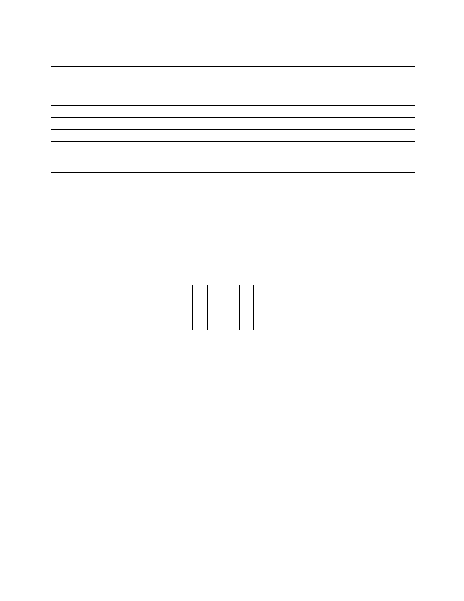
3. Measurements obtained using production test board described in Figure 5.
Input
50
Input
Transmission Line
Including
Gate Bias T
(0.3 dB loss)
Input
Matching Circuit
_mag = 0.13
_ang = 113
�
(0.3 dB loss)
50
Output
Transmission Line
Including
Gate Bias T
(0.5 dB loss)
DUT
Output
Figure 5. Block diagram of 2 GHz production test board used for Noise Figure, Associated Gain, P1dB, and OIP3 measurements. This circuit
represents a trade-off between an optimal noise match and a realizable match based on production test requirements. Circuit losses have been
de-embedded from actual measurements.
4
ATF-331M4 Typical Performance Curves
Notes:
1. Measurements made on fixed tuned
production test board that was tuned for
optimal gain match with reasonable noise
figure at 4V 60 mA bias. This circuit
represents a trade-off between an optimal
noise match, maximum gain match and a
realizable match based on production test
board requirements. Circuit losses have been
de-embedded from actual measurements.
2. Quiescent drain current, Idsq, is set with zero
RF drive applied. As P1dB is approached, the
drain current may increase or decrease
depending on frequency and dc bias point. At
lower values of Idsq the device is running
closer to class B as power output approaches
P1dB. This results in higher P1dB and higher
PAE (power added efficiency) when compared
to a device that is driven by a constant
current source as is typically done with active
biasing.
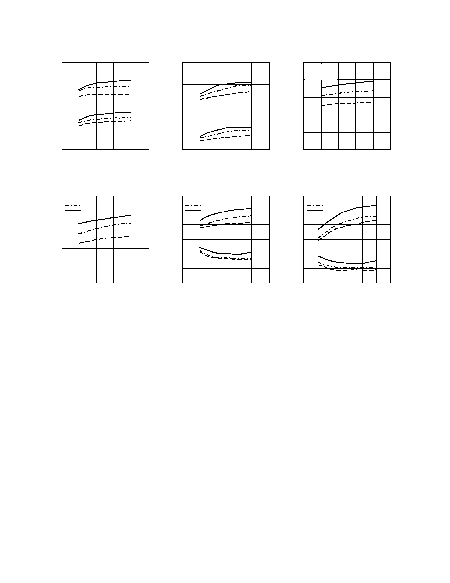
Figure 8. P1dB vs. Bias
[1,2]
2 GHz.
I
dsq
(mA)
P1dB (dBm)
0
100
40
20
80
60
2 V
3 V
4 V
25
20
15
10
5
0
Figure 10. NF & Gain vs. Bias
[1]
at 2 GHz.
I
d
(mA)
GAIN (dB)
NOISE FIGURE (dB)
0
100
40
20
80
60
2 V
3 V
4 V
16
15
14
13
12
11
10
1.4
1.2
1.0
0.8
0.6
0.4
0.2
Figure 6. OIP3, IIP3 & Bias
[1]
at 2 GHz.
I
ds
(mA)
OIP3, IIP3 (dBm)
0
100
40
20
80
60
2 V
3 V
4 V
40
30
20
10
0
Figure 7. OIP3, IIP3 & Bias
[1]
at 900 MHz.
I
ds
(mA)
OIP3, IIP3 (dBm)
0
100
40
20
80
60
2 V
3 V
4 V
40
30
20
10
0
Figure 9. P1dB vs. Bias
[1]
900 MHz.
I
dsq
(mA)
P1dB (dBm)
0
100
40
20
80
60
2 V
3 V
4 V
25
20
15
10
5
0
Figure 11. NF & Gain vs. Bias
[1]
at 900 MHz.
I
d
(mA)
GAIN (dB)
NOISE FIGURE (dB)
0
120
40
20
80
100
60
2 V
3 V
4 V
22
21
20
19
18
17
16
1.4
1.2
1.0
0.8
0.6
0.4
0.2
5
Notes:
1. Measurements made on fixed tuned
production test board that was tuned for
optimal gain match with reasonable noise
figure at 4V 60 mA bias. This circuit
represents a trade-off between an optimal
noise match, maximum gain match and a
realizable match based on production test
board requirements. Circuit losses have been
de-embedded from actual measurements.
2. Quiescent drain current, Idsq, is set with zero
RF drive applied. As P1dB is approached, the
drain current may increase or decrease
depending on frequency and dc bias point. At
lower values of Idsq the device is running
closer to class B as power output approaches
P1dB. This results in higher P1dB and higher
PAE (power added efficiency) when compared
to a device that is driven by a constant
current source as is typically done with active
biasing.
ATF-331M4 Typical Performance Curves, continued
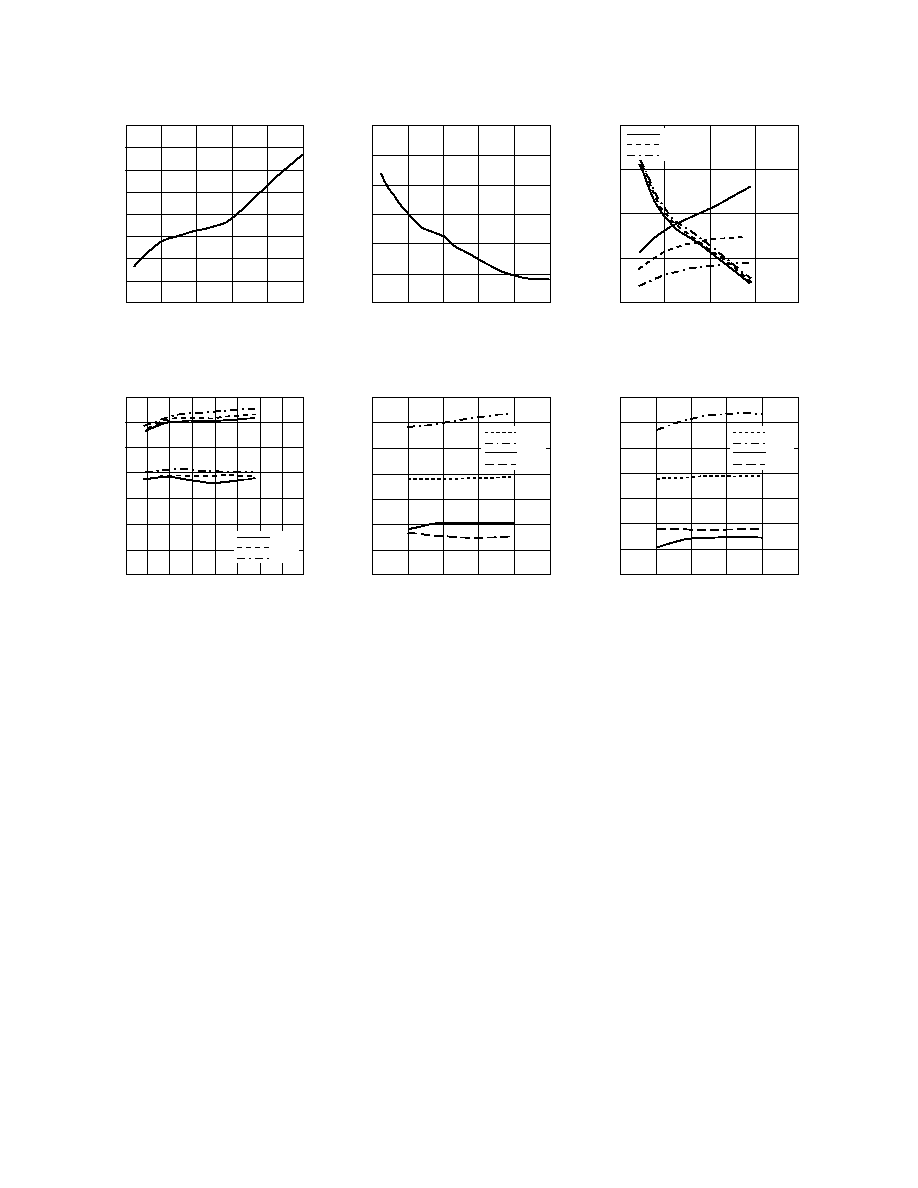
Figure 12. Fmin vs. Frequency at 4 V, 60 mA.
FREQUENCY (GHz)
Fmin (dB)
0
10
4
2
8
6
1.6
1.4
1.2
1.0
0.8
0.6
0.4
0.2
0
Figure 14. Fmin & Ga vs. Frequency and Temp.
Vd = 4 V , Ids = 60 mA.
FREQUENCY (GHz)
GAIN (dB)
NOISE FIGURE (dB)
0
8
4
2
6
85
�
C
25
�
C
-40
�
C
25
20
15
10
5
2.0
1.5
1.0
0.5
0
Figure 15. P1dB, OIP3 vs. Frequency and
Temp at Vd = 4 V , Ids = 60 mA.
FREQUENCY (GHz)
P1dB, OIP3 (dBm)
0
8
4
5
7
2
1
3
6
85
�
C
25
�
C
-40
�
C
35
30
25
20
15
10
5
0
Figure 16. OIP3, P1dB, NF and Gain vs.
Bias
[1,2]
at 3.9 GHz.
I
dsq
(mA)
OIP3, P1dB (dBm), GAIN (dB)
NOISE FIUGRE (dB)
0
100
40
20
80
60
P 1 d B
O I P 3
G a i n
N F
35
30
25
20
15
10
5
0
3.5
3.0
2.5
2.0
1.5
1.0
0.5
0
Figure 13. Associated Gain vs. Frequency
at 4 V , 60 mA.
FREQUENCY (GHz)
GAIN (dB)
0
10
4
2
8
6
30
25
20
15
10
5
0
Figure 17. OIP3, P1dB, NF at 5.8 GHz.
I
dsq
(mA)
OIP3, P1dB (dBm), GAIN (dB)
NOISE FIGURE (dB)
0
100
40
20
80
60
P 1 d B
O I P 3
G a i n
N F
35
30
25
20
15
10
5
0
3.5
3.0
2.5
2.0
1.5
1.0
0.5
0