 | –≠–ª–µ–∫—Ç—Ä–æ–Ω–Ω—ã–π –∫–æ–º–ø–æ–Ω–µ–Ω—Ç: ATF-36077 | –°–∫–∞—á–∞—Ç—å:  PDF PDF  ZIP ZIP |
Document Outline
- List of Figures
- 1. ATF-36077 Optimum Noise Figure and Associated Gain vs. Frequency
- 2. Maximum Available Gain, Maximum Stable Gain and Insertion Power Gain vs. Frequency
- Features
- Applications
- Description
- 77 Package
- Pin Configuration
- ATF-36077 Absolute Maximum Ratings
- ATF-36077 Electrical Specifications,
- ATF-36077 Characterization Information,
- ATF-36077 Typical Scattering Parameters
- ATF-36077 Typical çOffé Scattering Parameters
- ATF-36077 Typical Noise Parameters,
- 77 Package Dimensions
- Part Number Ordering Information
5-75
1
GATE
3
DRAIN
2
SOURCE
4
SOURCE
360
ATF-36077
2≠18 GHz Ultra Low Noise
Pseudomorphic HEMT
Technical Data
Features
∑ PHEMT Technology
∑ Ultra-Low Noise Figure:
0.5 dB Typical at 12 GHz
0.3 dB Typical at 4 GHz
∑ High Associated Gain:
12 dB Typical at 12 GHz
17 dB Typical at 4 GHz
∑ Low Parasitic Ceramic
Microstrip Package
∑ Tape-and-Reel Packing
Option Available
Applications
∑ 12 GHz DBS LNB (Low Noise
Block)
∑ 4 GHz TVRO LNB (Low Noise
Block)
∑ Ultra-Sensitive Low Noise
Amplifiers
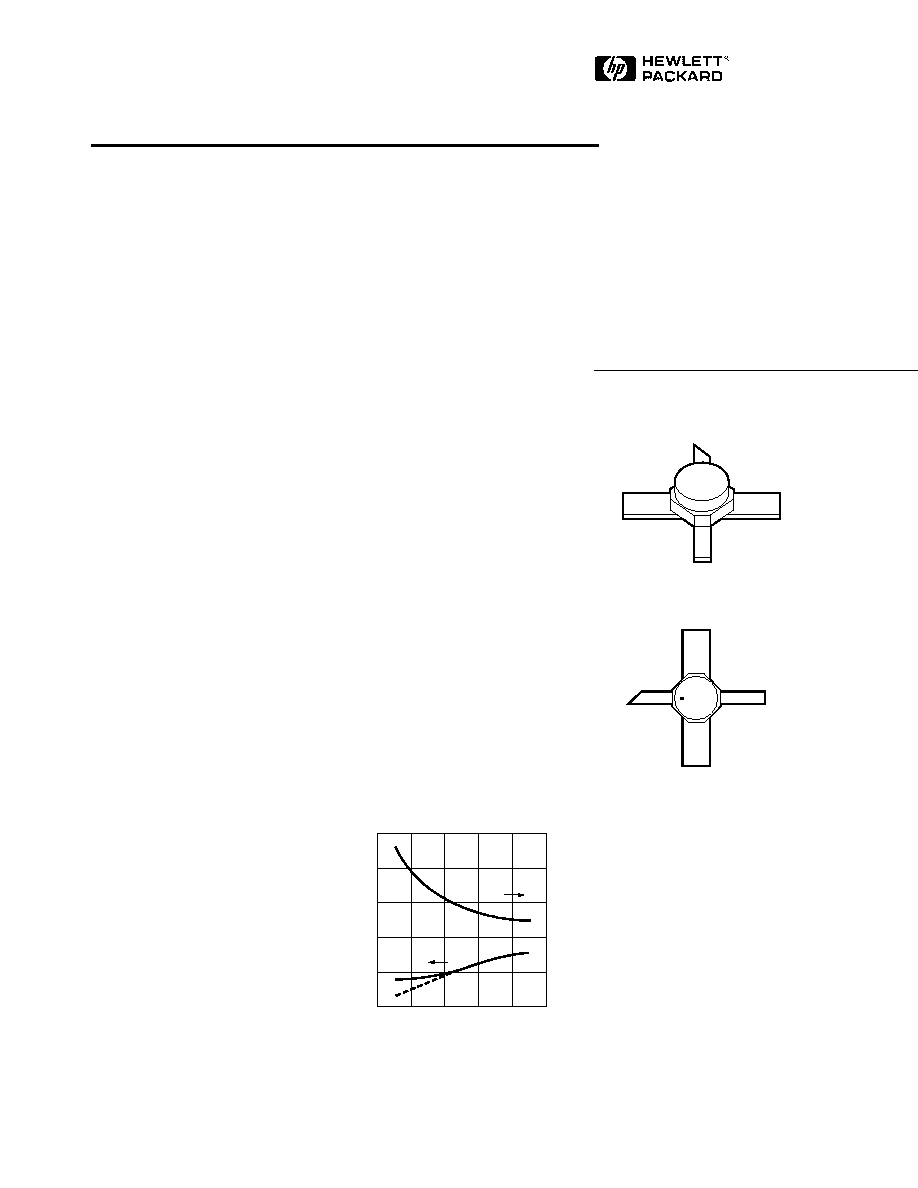
Figure 1. ATF-36077 Optimum Noise
Figure and Associated Gain vs.
Frequency for V
DS
= 1.5 V, I
D
= 10 mA.
Pin Configuration
77 Package
NOISE FIGURE (dB)
0
0
FREQUENCY (GHz)
8
16
20
1.2
0.8
0.4
4
12
Ga
ASSOCIATED GAIN (dB)
NF
10
15
20
25
[1]
Note: 1.
See Noise Parameter Table.
Description
Hewlett-Packard's ATF-36077 is
an ultra-low-noise Pseudomorphic
High Electron Mobility Transistor
(PHEMT), packaged in a low
parasitic, surface-mountable
ceramic package. Properly
matched, this transistor will
provide typical 12 GHz noise
figures of 0.5 dB, or typical 4 GHz
noise figures of 0.3 dB. Addition-
ally, the ATF-36077 has very low
noise resistance, reducing the
sensitivity of noise performance
to variations in input impedance
match, making the design of
broadband low noise amplifiers
much easier. The premium
sensitivity of the ATF-36077
makes this device the ideal choice
for use in the first stage of
extremely low noise cascades.
The repeatable performance and
consistency make it appropriate
for use in Ku-band Direct Broad-
cast Satellite (DBS) Television
systems, C-band Television
Receive Only (TVRO) LNAs, or
other low noise amplifiers
operating in the 2-18 GHz
frequency range.
This GaAs PHEMT device has a
nominal 0.2 micron gate length
with a total gate periphery (width)
of 200 microns. Proven gold based
metalization systems and nitride
passivation assure rugged, reliable
devices.
5965-8726E
5-76
ATF-36077 Electrical Specifications,
T
C
= 25
∞
C, Z
O
= 50
,
V
ds
= 1.5 V, I
ds
= 10 mA, (unless otherwise noted).
Symbol
Parameters and Test Conditions
Units
Min.
Typ.
Max.
NF
Noise Figure
[1]
f = 12.0 GHz
dB
0.5
0.6
G
A
Gain at NF
[1]
f = 12.0 GHz
dB
11.0
12.0
g
m
Transconductance
V
DS
= 1.5 V, V
GS
= 0 V
mS
50
55
I
dss
Saturated Drain Current
V
DS
= 1.5 V, V
GS
= 0 V
mA
15
25
45
V
p 10 %
Pinch-off Voltage
V
DS
= 1.5 V, I
DS
= 10% of I
dss
V
-1.0
-0.35
-0.15
Note:
1. Measured in a fixed tuned environment with
source = 0.54 at 156
∞
;
load = 0.48 at 167
∞
.
Thermal Resistance
[2,3]
:
ch-c
= 60
∞
C/W
Notes:
1. Operation of this device above any one
of these parameters may cause
permanent damage.
2. Measured at P
diss
= 15 mW and
T
ch
= 100
∞
C.
3. Derate at 16.7 mW/
∞
C for T
C
> 139
∞
C.
ATF-36077 Absolute Maximum Ratings
Absolute
Symbol
Parameter
Units
Maximum
[1]
V
DS
Drain ≠ Source Voltage
V
+3
V
GS
Gate ≠ Source Voltage
V
-3
V
GD
Gate-Drain Voltage
V
-3.5
I
D
Drain Current
mA
I
dss
P
T
Total Power Dissipation
[3]
mW
180
P
in max
RF Input Power
dBm
+10
T
ch
Channel Temperature
∞
C
150
T
STG
Storage Temperature
∞
C
-65 to 150
ATF-36077 Characterization Information,
T
C
= 25
∞
C, Z
O
= 50
,
V
ds
= 1.5 V, I
ds
= 10 mA, (unless otherwise noted).
Symbol
Parameters and Test Conditions
Units
Typ.
NF
Noise Figure (Tuned Circuit)
f = 4 GHz
dB
0.3
[2]
f = 12 GHz
dB
0.5
G
A
Gain at Noise Figure (Tuned Circuit)
f = 4 GHz
dB
17
f = 12 GHz
dB
12
S
12 off
Reverse Isolation
f = 12 GHz, V
DS
= 1.5 V, V
GS
= -2 V
dB
14
P
1dB
Output Power at 1 dB Gain Compression
f = 4 GHz
dBm
5
f = 12 GHz
dBm
5
V
GS 10 mA
Gate to Source Voltage for I
DS
= 10 mA
V
DS
= 1.5 V
V
-0.2
Note:
2. See noise parameter table.
5-77
ATF-36077 Typical Scattering Parameters,
Common Source, Z
O
= 50
, V
DS
= 1.5 V, I
D
= 10 mA
Freq.
S
11
S
21
S
12
S
22
GHz
Mag.
Ang.
dB
Mag.
Ang.
dB
Mag.
Ang.
Mag.
Ang.
1.0
0.99
-17
14.00
5.010
163
-36.08
0.016
78
0.60
-14
2.0
0.97
-33
13.81
4.904
147
-30.33
0.030
66
0.59
-28
3.0
0.94
-49
13.53
4.745
132
-27.25
0.043
54
0.57
-41
4.0
0.90
-65
13.17
4.556
116
-25.32
0.054
43
0.55
-54
5.0
0.86
-79
12.78
4.357
102
-24.04
0.063
33
0.53
-66
6.0
0.82
-93
12.39
4.162
88
-23.17
0.069
24
0.50
-78
7.0
0.78
-107
12.00
3.981
75
-22.58
0.074
16
0.48
-89
8.0
0.75
-120
11.64
3.820
62
-22.17
0.078
8
0.46
-99
9.0
0.72
-133
11.32
3.682
49
-21.90
0.080
1
0.44
-109
10.0
0.69
-146
11.04
3.566
37
-21.71
0.082
-6
0.42
-119
11.0
0.66
-159
10.81
3.473
25
-21.57
0.083
-13
0.40
-129
12.0
0.63
-172
10.63
3.401
13
-21.44
0.085
-19
0.38
-139
13.0
0.61
175
10.50
3.349
1
-21.32
0.086
-25
0.37
-149
14.0
0.60
161
10.41
3.315
-12
-21.19
0.087
-32
0.35
-160
15.0
0.58
147
10.36
3.296
-24
-21.04
0.089
-39
0.33
-171
16.0
0.57
131
10.34
3.289
-37
-20.87
0.091
-47
0.31
177
17.0
0.56
114
10.34
3.289
-50
-20.69
0.092
-55
0.29
164
18.0
0.57
97
10.35
3.291
-64
-20.53
0.094
-65
0.26
148
ATF-36077 Typical "Off" Scattering Parameters,
Common Source, Z
O
= 50
, V
DS
= 1.5 V, I
D
= 0 mA, V
GS
= -2 V
Freq.
S
11
S
21
S
21
S
22
GHz
Mag.
Ang.
dB
Mag.
Ang.
dB
Mag.
Ang.
Mag.
Ang.
11.0
0.96
-139
-14.2
0.19
-43
-14.2
0.19
-43
0.97
-125
12.0
0.95
-152
-14.0
0.20
-56
-14.0
0.20
-56
0.97
-137
13.0
0.94
-166
-13.8
0.20
-69
-13.8
0.20
-68
0.96
-149

5-78
ATF-36077 Typical Noise Parameters,
Common Source, Z
O
= 50
, V
DS
= 1.5 V, I
D
= 10 mA
Freq.
F
min
[1]
opt
R
n
/ Z
o
GHz
dB
Mag.
Ang.
-
1
0.30
0.95
12
0.40
2
0.30
0.90
25
0.20
4
0.30
0.81
51
0.17
6
0.30
0.73
76
0.13
8
0.37
0.66
102
0.09
10
0.44
0.60
129
0.05
12
0.50
0.54
156
0.03
14
0.56
0.48
-174
0.02
16
0.61
0.43
-139
0.05
18
0.65
0.39
-100
0.09
Note:
1. The F
min
values at 2,4, and 6 GHz have been adjusted to reflect expected circuit losses
that will be encountered when matching to the optimum reflection coefficient (
opt
) at
these frequencies. The theoretical F
min
values for these frequencies are: 0.10 dB at
2 GHz, 0.20 dB at 4 GHz, and 0.29 dB at 6 GHz. Noise parameters are derived from
associated s parameters, packaged device measurements at 12 GHz, and die level
measurements from 6 to 18 GHz.
Part Number Ordering Information
Part Number
No. of Devices
Container
ATF-36077-TRl
[2]
1000
7" Reel
ATF-36077-STR
10
strip
Note:
2. For more information, see "Tape and Reel Packaging for Semiconductor Devices," in
"Communications Components" Designer`s Catalog.
77 Package Dimensions
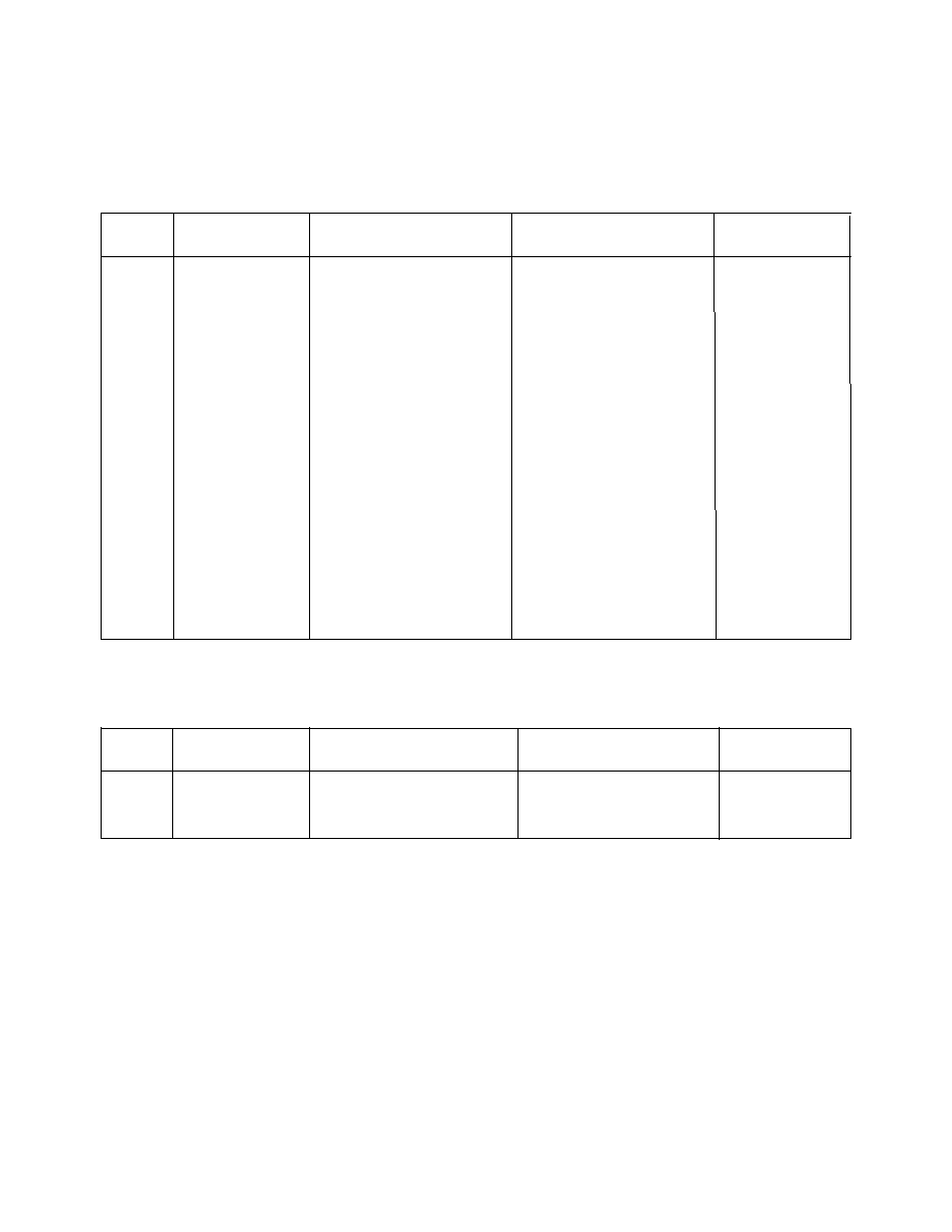
Figure 2. Maximum Available Gain,
Maximum Stable Gain and Insertion
Power Gain vs. Frequency. V
DS
= 1.5 V,
I
D
= 10 mA.
GAIN (dB)
0
25
0
FREQUENCY (GHz)
8
16
20
20
15
10
5
4
12
S21
MSG MAG
1.02
(0.040)
.51
(0.020)
1.78
(0.070)
1.22
(0.048)
.53
(0.021)
5.28
(0.208)
.10
(0.004)
TYPICAL DIMENSIONS ARE IN MILLIMETERS (INCHES).
4
2
1
3
GATE
DRAIN
SOURCE
SOURCE
1.75
(0.069)
360