 | –≠–ª–µ–∫—Ç—Ä–æ–Ω–Ω—ã–π –∫–æ–º–ø–æ–Ω–µ–Ω—Ç: ATF-36163 | –°–∫–∞—á–∞—Ç—å:  PDF PDF  ZIP ZIP |
Document Outline
- List of Figures
- 1. ATF-36163 Minimum Noise Figure and Associated Gain vs. Frequency for V DS = 1.5 V, I D = 10 mA.
- 2. Maximum Available Gain, Maximum Stable Gain & Insertion Power Gain vs. Frequency for V DS = 1.5 V, I D = 10 mA.
- 3. ATF-36163 Minimum Noise Figure and Associated Gain vs. Frequency for V DS = 1.5 V, I D = 15 mA.
- 4. Maximum Available Gain, Maximum Stable Gain & Insertion Power Gain vs. Frequency for V DS = 1.5 V, I D = 15 mA.
- 5. ATF-36163 Minimum Noise Figure and Associated Gain vs. Frequency for V DS = 2.0 V, I D = 10 mA.
- 6. Maximum Available Gain, Maximum Stable Gain & Insertion Power Gain vs. Frequency for V DS = 2.0 V, I D = 10 mA.
- 7. ATF-36163 Minimum Noise Figure and Associated Gain vs. Frequency for V DS = 2 V, I D = 15 mA.
- 8. Maximum Available Gain, Maximum Stable Gain & Insertion Power Gain vs. Frequency for V DS = 2 V, I D = 15 mA.
- 9. Smith Chart with Noise Figure and Available Gain Circles at 12 GHz, V DS = 1.5 V, I D = 10 mA.
- 10. Reference Planes.
- 11. PCB Pad Layout (Dimensions in Inches).
- Features
- Applications
- Surface Mount Package
- Pin Connections and Package Marking
- Description
- ATF-36163 Absolute Maximum Ratings [1]
- ATF-36163 Electrical Specifications
- ATF-36163 Typical Parameters
- ATF-36163 Typical Scattering Parameters, Common Source, ZO = 50 W, VDS = 1.5 V, ID = 10 mA
- ATF-36163 Typical Noise Parameters Common Source, ZO = 50 W, VDS = 1.5 V, ID = 10 mA
- ATF-36163 Typical Scattering Parameters, Common Source, ZO = 50 W, VDS = 1.5 V, ID = 15 mA
- ATF-36163 Typical Noise Parameters Common Source, ZO = 50 W, VDS = 1.5 V, ID = 15 mA
- ATF-36163 Typical Scattering Parameters, Common Source, ZO = 50 W, VDS = 2.0 V, ID = 10 mA
- ATF-36163 Typical Noise Parameters Common Source, ZO = 50 W, VDS = 2.0 V, ID = 10 mA
- ATF-36163 Typical Scattering Parameters, Common Source, ZO = 50 W, VDS = 2 V, ID = 15 mA
- ATF-36163 Typical Noise Parameters Common Source, ZO = 50 W, VDS = 2.0 V, ID = 15 mA
- ATF-36163 Typical çOffé Scattering Parameters, Common Source, ZO = 50 W,VDS =0 V, V GS=0V
- ATF-36163 Typical çOffé Scattering Parameters, Common Source, ZO = 50 W, VDS = 2.0 V, V GS=-1.5V
- Phase Reference Planes
- SOT-363 PCB Layout
- Package Dimensions - Outline 63 (SOT-363/SC-70)
- Part Number Ordering Information
- Device Orientation
- Tape Dimensions and Product Orientation - For Outline 63
5-79
1.5 ≠ 18 GHz Surface Mount
Pseudomorphic HEMT
Technical Data
ATF-36163
Features
∑ Low Minimum Noise Figure:
1 dB Typical at 12 GHz
0.6 dB Typical at 4 GHz
∑ Associated Gain:
9.4 dB Typical at 12 GHz
15.8 dB Typical at 4 GHz
∑ Maximum Available Gain:
11 dB Typical at 12 GHz
17 dB Typical at 4 GHz
∑ Low Cost Surface Mount
Small Plastic Package
∑ Tape-and-Reel Packaging
Option Available
Applications
∑ 12 GHz DBS Downconverters
∑ 4 GHz TVRO Downconverters
∑ S or L Band Low Noise
Amplifiers
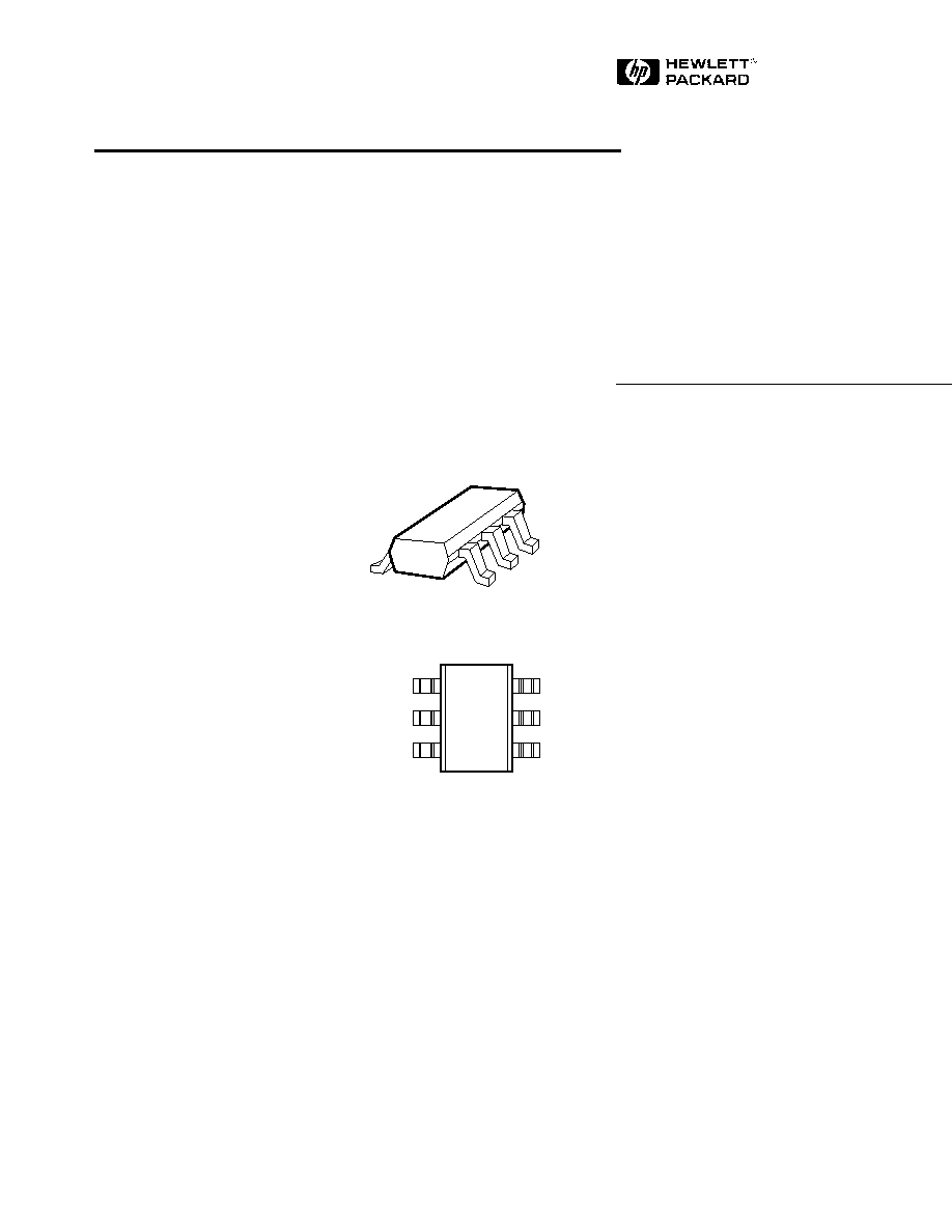
Surface Mount Package
SOT-363 (SC-70)
Additionally, the ATF-36163 has
low noise-resistance, which
reduces the sensitivity of noise
performance to variations in
input impedance match. This
feature makes the design of broad
band low noise amplifiers much
easier. The performance of the
ATF-36163 makes this device the
ideal choice for use in the 2nd or
3rd stage of low noise cascades.
The repeatable performance and
consistency make it appropriate
for use in Ku-band Direct
Broadcast Satellite (DBS) TV
systems, C-band TV Receive Only
(TVRO) LNAs, Multichannel
Multipoint Distribution Systems
(MMDS), X-band Radar detector
and other low noise amplifiers
operating in the 1.5 ≠ 18 GHz
frequency range.
This GaAs PHEMT device has a
nominal 0.2 micron gate length
with a total gate periphery
(width) of 200 microns. Proven
gold-based metallization system
and nitride passivation assure
rugged, reliable devices.
Description
The Hewlett-Packard ATF-36163
is a low-noise Pseudomorphic
High Electron Mobility Transistor
(PHEMT), in the SOT-363 (SC-70)
package. When optimally matched
for minimum noise figure, it will
provide a noise figure of 1 dB at
12 GHz and 0.6 dB at 4 GHz.
Pin Connections and
Package Marking
DRAIN
SOURCE
36
SOURCE
SOURCE
GATE
SOURCE
Note: Package marking provides
orientation and identification.
5965-4747E
5-80
ATF-36163 Absolute Maximum Ratings
[1]
Absolute
Symbol
Parameter
Units
Maximum
V
DS
Drain - Source Voltage
V
+3
V
GS
Gate - Source Voltage
V
-3
V
GD
Gate Drain Voltage
V
-3.5
I
D
Drain Current
mA
I
dss
P
T
Total Power Dissipation
mW
180
P
in max
RF Input Power
dBm
+10
T
CH
Channel Temperature
∞
C
150
T
STG
Storage Temperature
∞
C
-65 to 150
Thermal Resistance:
ch-c
= 160
∞
C/W
Note:
1. Operation of this device above any one
of these parameters may cause
permanent damage.
ATF-36163 Typical Parameters
T
C
= 25
∞
C, Z
O
= 50
, V
ds
= 2 V, I
ds
= 15 mA, (unless otherwise noted).
Symbol
Parameters and Test Conditions
Units
Typ.
F
min
Minimum Noise Figure (
source
=
opt
)
f = 4 GHz
dB
0.6
f = 12 GHz
dB
1.0
G
a
Associated Gain
f = 4 GHz
dB
15.8
f = 12 GHz
dB
9.4
G
max
Maximum Available Gain
[1]
f = 4 GHz
dB
17.2
f = 12 GHz
dB
10.9
P
1dB
Output Power at 1 dB Gain Compression
f = 4 GHz
dBm
5
under the power matched condition
f = 12 GHz
dBm
5
V
GS
Gate to Source Voltage for I
DS
= 15 mA
V
DS
= 2.0 V
V
-0.2
Note:
1. G
max
= MAG for K > 1 and G
max
= MSG for K
1, which is shown on the S-parameters tables.
ATF-36163 Electrical Specifications
T
C
= 25
∞
C, Z
O
= 50
, V
ds
= 1.5 V, I
ds
= 10 mA, (unless otherwise noted).
Symbol
Parameters and Test Conditions
Units
Min.
Typ.
Max.
NF
Noise Figure
[1]
f =12.0 GHz
dB
1.2
1.4
[1]
G
Gain at NF
[1]
f = 12.0 GHz
dB
9
10
g
m
Transconductance
V
DS
= 1.5 V, V
GS
= 0 V
mS
50
60
I
dss
Saturated Drain Current
V
DS
= 1.5 V, V
GS
= 0 V
mA
15
25
40
V
p 10%
Pinchoff Voltage
V
DS
= 1.5 V, I
DS
= 10% of I
dss
V
-1.0
-0.35
-0.15
BV
GDO
Gate Drain Breakdown Voltage
I
G
= 30
µ
A
V
-3.5
Note:
1. Measured in a test circuit tuned for a typical device.

5-81
ATF-36163 Typical Noise Parameters
Common Source, Z
O
= 50
, V
DS
= 1.5 V, I
D
= 10 mA
Freq.
F
min
G
a
opt
R
n
/Z
O
GHz
dB
dB
Mag.
Ang.
-
2
0.48
18.77
0.78
28
0.38
3
0.53
16.75
0.75
41
0.32
4
0.57
15.17
0.68
55
0.26
5
0.61
14.14
0.60
71
0.20
6
0.66
13.23
0.55
88
0.15
7
0.71
12.06
0.48
105
0.12
8
0.77
11.22
0.38
119
0.10
9
0.83
10.50
0.32
138
0.07
10
0.89
10.02
0.23
170
0.07
11
0.97
9.44
0.18
-141
0.09
12
1.05
8.92
0.20
-92
0.13
13
1.14
8.45
0.26
-46
0.21
14
1.24
8.12
0.36
-16
0.32
15
1.37
8.08
0.48
4
0.44
16
1.51
8.11
0.59
19
0.60
17
1.68
7.97
0.64
34
0.79
18
1.89
7.59
0.70
51
1.15
ATF-36163 Typical Scattering Parameters,
Common Source, Z
O
= 50
, V
DS
= 1.5 V, I
D
= 10 mA
Freq.
S
11
S
21
S
12
S
22
K
G
max
[1]
GHz
Mag.
Ang.
dB
Mag.
Ang.
dB
Mag.
Ang.
Mag.
Ang.
--
dB
0.5
0.99
-11
12.85
4.39
168
-37.72
0.01
79
0.51
-9
0.11
25.24
1
0.98
-22
12.70
4.31
158
-31.70
0.03
71
0.50
-18
0.17
22.26
2
0.96
-42
12.48
4.21
138
-26.02
0.05
55
0.48
-36
0.24
19.28
3
0.93
-61
12.37
4.15
118
-22.73
0.07
40
0.45
-53
0.33
17.56
4
0.87
-83
12.30
4.12
97
-20.45
0.10
23
0.40
-71
0.43
16.38
5
0.81
-106
12.16
4.06
76
-18.71
0.12
6
0.34
-92
0.51
15.43
6
0.75
-131
11.94
3.95
55
-17.52
0.13
-12
0.27
-116
0.58
14.73
7
0.67
-158
11.47
3.75
33
-16.77
0.15
-30
0.18
-144
0.69
14.12
8
0.61
176
11.01
3.55
12
-16.36
0.15
-45
0.10
174
0.79
13.69
9
0.57
143
10.47
3.34
-10
-15.97
0.16
-61
0.12
93
0.85
13.22
10
0.57
108
9.66
3.04
-32
-15.92
0.16
-77
0.22
53
0.91
12.80
11
0.59
76
8.53
2.67
-54
-16.48
0.15
-93
0.33
28
0.99
12.50
12
0.63
50
7.39
2.34
-74
-17.14
0.14
-106
0.41
9
1.07
10.65
13
0.67
26
6.10
2.02
-93
-18.27
0.12
-119
0.49
-8
1.18
9.64
14
0.72
6
4.81
1.74
-111
-19.74
0.10
-129
0.56
-22
1.30
8.99
15
0.78
-11
3.49
1.50
-128
-21.41
0.09
-138
0.63
-33
1.38
8.81
16
0.82
-24
2.20
1.29
-146
-23.10
0.07
-144
0.67
-43
1.44
8.70
17
0.87
-38
0.59
1.07
-164
-25.04
0.06
-151
0.73
-53
1.46
8.79
18
0.90
-52
-1.63
0.83
178
-29.12
0.04
-159
0.78
-65
1.80
8.58
Note:
1. G
max
= MAG for K > 1 and G
max
= MSG for K
1.
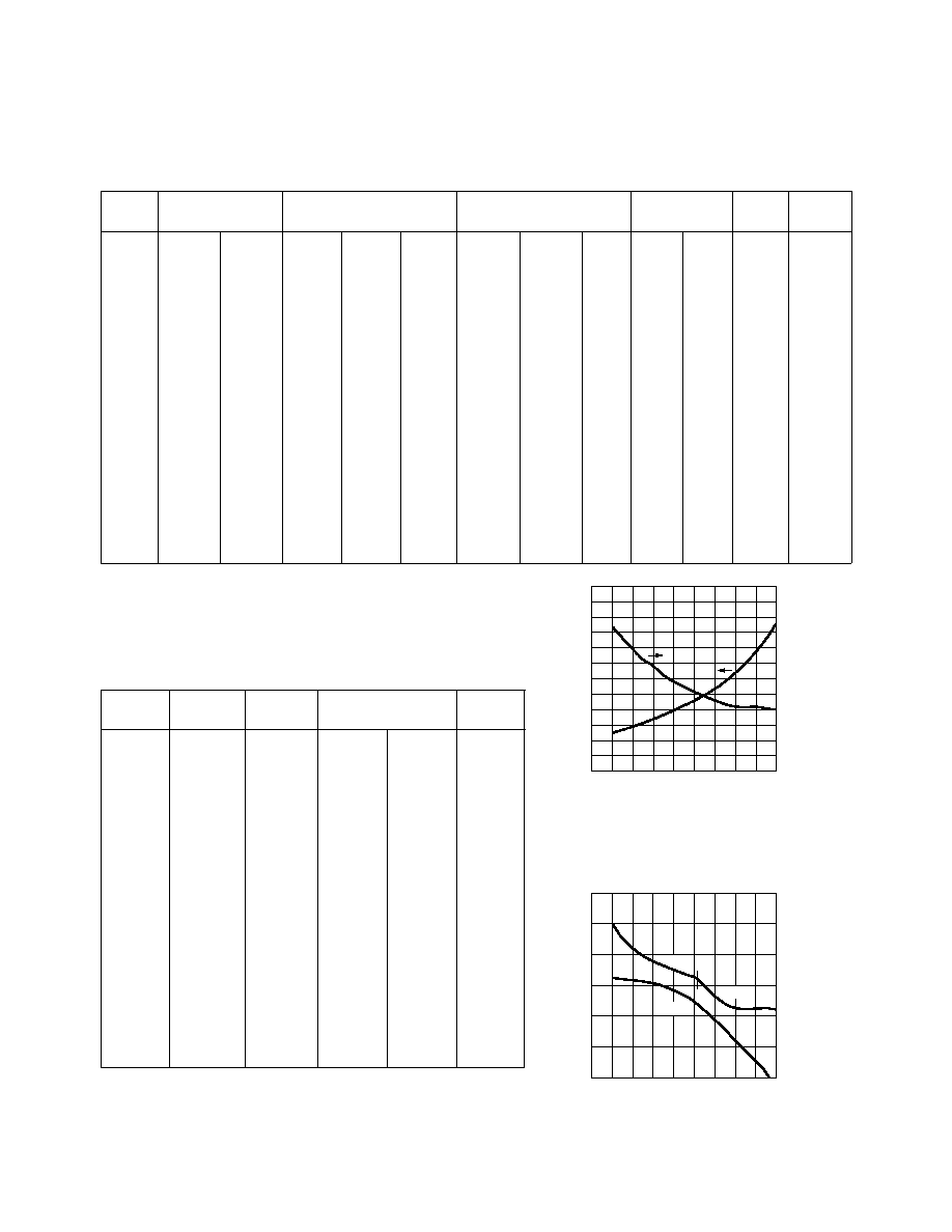
Figure 1. ATF-36163 Minimum Noise Figure and
Associated Gain vs. Frequency for
V
DS
= 1.5 V, I
D
= 10 mA.
Figure 2. Maximum Available Gain, Maximum
Stable Gain & Insertion Power Gain vs.
Frequency for V
DS
= 1.5 V, I
D
= 10 mA.
0
18
2.4
0
2
6
10 12
2.0
1.2
0.4
14
F
min
(dB)
FREQUENCY (GHz)
0.8
1.6
4
8
16
24
0
20
12
4
8
16
G
a
(dB)
0
18
24
0
2
6
10 12
20
12
4
14
GAIN (dB)
FREQUENCY (GHz)
8
16
4
8
16
MAG
MSG
|S21|
2
5-82
ATF-36163 Typical Scattering Parameters,
Common Source, Z
O
= 50
, V
DS
= 1.5 V, I
D
= 15 mA
Freq.
S
11
S
21
S
12
S
22
K
G
max
[1]
GHz
Mag.
Ang.
dB
Mag.
Ang.
dB
Mag.
Ang.
Mag.
Ang.
--
dB
0.5
0.99
-12
13.56
4.76
168
-38.42
0.01
79
0.45
-9
0.12
25.82
1
0.98
-22
13.40
4.68
157
-32.40
0.02
71
0.45
-18
0.18
22.86
2
0.96
-43
13.16
4.55
137
-26.56
0.05
56
0.43
-36
0.26
19.87
3
0.92
-63
13.00
4.47
116
-23.22
0.07
40
0.40
-52
0.35
18.13
4
0.86
-85
12.87
4.40
96
-21.01
0.09
24
0.35
-70
0.46
16.94
5
0.80
-108
12.68
4.30
75
-19.25
0.11
7
0.28
-92
0.55
15.98
6
0.74
-133
12.38
4.16
53
-18.13
0.12
-11
0.21
-116
0.62
15.25
7
0.66
-160
11.85
3.91
31
-17.39
0.14
-28
0.13
-146
0.74
14.62
8
0.59
173
11.33
3.68
11
-16.95
0.14
-42
0.06
156
0.84
14.14
9
0.56
141
10.74
3.44
-11
-16.54
0.15
-58
0.12
73
0.90
13.63
10
0.56
106
9.89
3.12
-33
-16.42
0.15
-73
0.23
44
0.95
13.16
11
0.59
74
8.74
2.74
-54
-16.83
0.14
-88
0.34
23
1.03
11.78
12
0.63
49
7.59
2.40
-74
-17.39
0.14
-102
0.42
6
1.10
10.62
13
0.68
25
6.29
2.06
-93
-18.42
0.12
-115
0.50
-10
1.19
9.72
14
0.73
5
5.01
1.78
-110
-19.74
0.10
-124
0.57
-23
1.29
9.15
15
0.79
-12
3.70
1.53
-127
-21.31
0.09
-133
0.64
-34
1.35
8.99
16
0.83
-25
2.43
1.32
-144
-22.85
0.07
-139
0.68
-44
1.39
8.93
17
0.87
-38
0.84
1.10
-163
-24.73
0.06
-148
0.73
-54
1.39
9.06
18
0.91
-53
-1.33
0.86
180
-28.87
0.04
-155
0.78
-66
1.67
8.92
Note:
1. G
max
= MAG for K > 1 and G
max
= MSG for K
1.
Figure 3. ATF-36163 Minimum Noise Figure and
Associated Gain vs. Frequency for
V
DS
= 1.5 V, I
D
= 15 mA.
Figure 4. Maximum Available Gain, Maximum
Stable Gain & Insertion Power Gain vs.
Frequency for V
DS
= 1.5 V, I
D
= 15 mA.
0
18
2.4
0
2
6
10 12
2.0
1.2
0.4
14
F
min
(dB)
FREQUENCY (GHz)
0.8
1.6
4
8
16
24
0
20
12
4
8
16
G
a
(dB)
0
18
24
0
2
6
10 12
20
12
4
14
GAIN (dB)
FREQUENCY (GHz)
8
16
4
8
16
MAG
MSG
|S21|
2
ATF-36163 Typical Noise Parameters
Common Source, Z
O
= 50
, V
DS
= 1.5 V, I
D
= 15 mA
Freq.
F
min
G
a
opt
R
n
/Z
O
GHz
dB
dB
Mag.
Ang.
-
2
0.49
18.87
0.84
28
0.38
3
0.54
17.20
0.74
42
0.31
4
0.58
15.75
0.66
57
0.25
5
0.63
14.49
0.59
72
0.19
6
0.68
13.61
0.54
90
0.15
7
0.73
12.36
0.46
106
0.11
8
0.79
11.54
0.37
121
0.09
9
0.85
10.82
0.30
140
0.08
10
0.91
10.32
0.21
174
0.08
11
0.99
9.73
0.17
-133
0.10
12
1.07
9.22
0.20
-83
0.14
13
1.17
8.68
0.26
-40
0.22
14
1.27
8.41
0.38
-12
0.34
15
1.40
8.36
0.49
7
0.46
16
1.54
8.37
0.60
21
0.64
17
1.72
8.10
0.62
35
0.85
18
1.93
8.00
0.71
52
1.18

5-83
ATF-36163 Typical Scattering Parameters,
Common Source, Z
O
= 50
, V
DS
= 2.0 V, I
D
= 10 mA
Freq.
S
11
S
21
S
12
S
22
K
Gmax
[1]
GHz
Mag.
Ang.
dB
Mag.
Ang.
dB
Mag. Ang.
Mag.
Ang.
≠
dB
0.5
0.99
-11
13.06
4.50
168
-37.72
0.01
79
0.55
-9
0.11
25.46
1
0.99
-22
12.90
4.42
158
-32.04
0.03
71
0.55
-18
0.16
22.46
2
0.96
-42
12.69
4.31
138
-26.38
0.05
56
0.53
-35
0.24
19.50
3
0.93
-62
12.57
4.25
118
-22.97
0.07
40
0.50
-52
0.32
17.77
4
0.87
-83
12.51
4.22
97
-20.72
0.09
23
0.44
-70
0.42
16.61
5
0.81
-106
12.38
4.16
76
-18.94
0.11
6
0.38
-90
0.51
15.67
6
0.75
-131
12.15
4.05
55
-17.79
0.13
-12
0.31
-112
0.58
14.98
7
0.67
-157
11.70
3.84
33
-17.08
0.14
-30
0.21
-137
0.69
14.38
8
0.60
176
11.25
3.65
13
-16.65
0.15
-44
0.13
-168
0.79
13.96
9
0.57
144
10.73
3.44
-10
-16.25
0.15
-60
0.10
115
0.85
13.50
10
0.56
109
9.95
3.14
-32
-16.25
0.15
-76
0.18
61
0.91
13.10
11
0.58
77
8.86
2.77
-53
-16.77
0.15
-91
0.29
32
1.00
12.52
12
0.62
50
7.75
2.44
-73
-17.39
0.14
-104
0.37
12
1.08
10.82
13
0.67
26
6.49
2.11
-93
-18.56
0.12
-117
0.46
-5
1.19
9.85
14
0.72
6
5.24
1.83
-110
-19.91
0.10
-126
0.53
-19
1.31
9.24
15
0.78
-10
3.96
1.58
-128
-21.51
0.08
-134
0.60
-30
1.38
9.07
16
0.82
-24
2.68
1.36
-146
-23.10
0.07
-139
0.65
-40
1.42
9.03
17
0.87
-37
1.08
1.13
-165
-24.88
0.06
-147
0.71
-50
1.38
9.28
18
0.91
-52
-1.16
0.88
177
-28.64
0.04
-153
0.78
-63
1.63
9.06
Figure 5. ATF-36163 Minimum Noise Figure and
Associated Gain vs. Frequency for
V
DS
= 2.0 V, I
D
= 10 mA.
Figure 6. Maximum Available Gain, Maximum
Stable Gain & Insertion Power Gain vs.
Frequency for V
DS
= 2.0 V, I
D
= 10 mA.
ATF-36163 Typical Noise Parameters
Common Source, Z
O
= 50
, V
DS
= 2.0 V, I
D
= 10 mA
Freq.
F
min
G
a
opt
R
n
/Z
O
GHz
dB
dB
Mag.
Ang.
-
2
0.46
18.60
0.84
28
0.38
3
0.50
16.75
0.76
41
0.31
4
0.54
15.55
0.67
56
0.25
5
0.59
14.20
0.61
70
0.20
6
0.63
13.37
0.55
88
0.15
7
0.68
12.12
0.49
103
0.12
8
0.74
11.35
0.39
118
0.10
9
0.80
10.59
0.33
135
0.07
10
0.86
10.11
0.23
165
0.07
11
0.94
9.57
0.17
-145
0.09
12
1.02
9.08
0.18
-93
0.12
13
1.11
8.59
0.24
-47
0.19
14
1.22
8.30
0.34
-16
0.30
15
1.35
8.29
0.47
5
0.42
16
1.51
8.32
0.58
19
0.57
17
1.69
8.07
0.60
34
0.76
18
1.92
7.68
0.66
50
1.10
0
18
2.4
0
2
6
10 12
2.0
1.2
0.4
14
F
min
(dB)
FREQUENCY (GHz)
0.8
1.6
4
8
16
24
0
20
12
4
8
16
G
a
(dB)
0
18
24
0
2
6
10 12
20
12
4
14
GAIN (dB)
FREQUENCY (GHz)
8
16
4
8
16
MAG
MSG
|S21|
2
Note:
1. G
max
= MAG for K > 1 and G
max
= MSG for K
1.