 | –≠–ª–µ–∫—Ç—Ä–æ–Ω–Ω—ã–π –∫–æ–º–ø–æ–Ω–µ–Ω—Ç: HBFP0420 | –°–∫–∞—á–∞—Ç—å:  PDF PDF  ZIP ZIP |
High Performance Isolated
Collector Silicon Bipolar
Transistor
Technical Data
Features
∑ Ideal for High Gain, Low
Noise Applications
∑ Transition Frequency
f
T
= 25 GHz
∑ Typical Performance at
1.8 GHz
Associated Gain of 17 dB
and Noise Figure of 1.1 dB
at 2 V and 5 mA
P
1dB
of 12 dBm at 2 V and
20 mA
∑ Can be Used Without
Impedance Matching
Applications
∑ LNA, Oscillator, Driver
Amplifier, Buffer Amplifier,
and Down Converter for
Cellular and PCS Handsets
and Cordless Telephones
∑ Oscillator for TV Delivery
and TVRO Systems up to
10 GHz
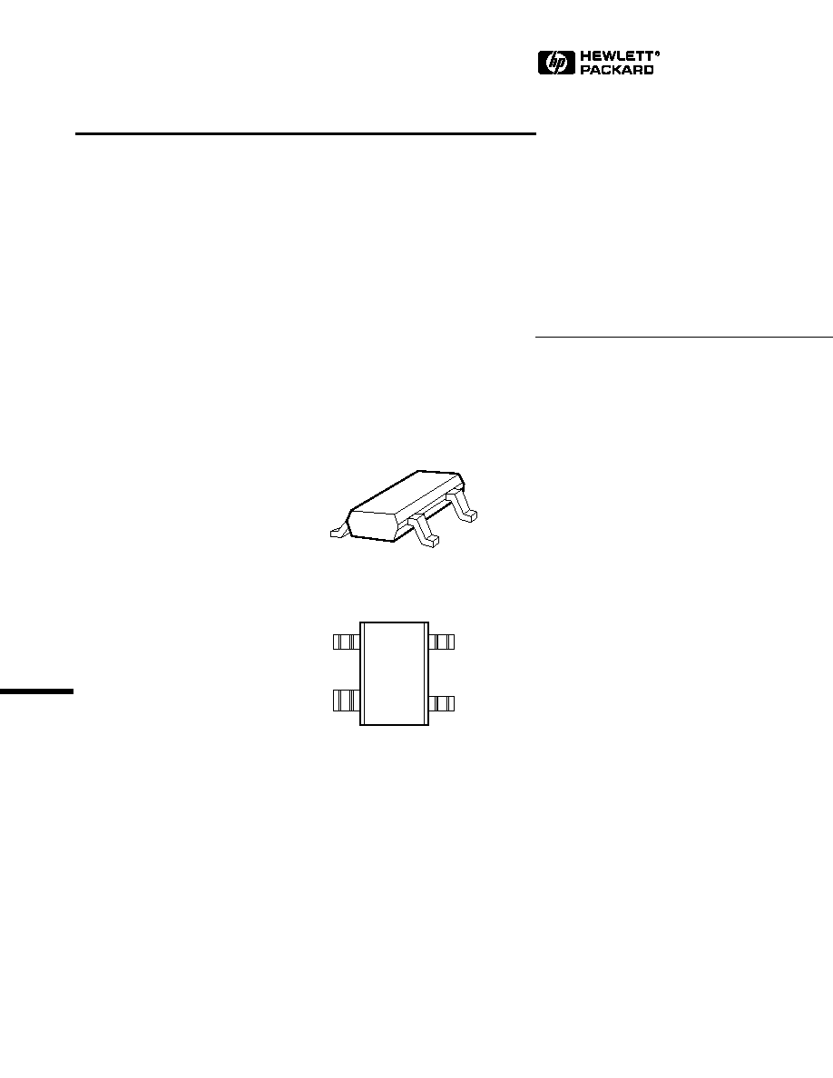
HBFP-0420
Description
Hewlett Packard's HBFP-0420 is a
high performance isolated
collector silicon bipolar junction
transistor housed in a 4-lead SC-70
(SOT-343) surface mount plastic
package.
HBFP-0420 provides an associated
gain of 17 dB, noise figure of
1.1 dB, and P
1dB
of 12 dBm at
1.8 GHz. Because of high gain and
low current characteristics,
HBFP-0420 is ideal for cellular/
PCS handsets
as well as for
C-Band and Ku-Band
applications.
This product is based on a 25 GHz
transition frequency fabrication
process, which enables the
products to be used for high
performance, low noise applica-
tions at 900 MHz, 1.9 GHz,
2.4 GHz, and beyond.
Surface Mount Plastic
Package/ SOT-343 (SC-70)
Outline 4T
Pin Configuration
Collector
Emitter
Base
03
Emitter
Note:
Package marking provides orientation
and identification.
2
HBFP-0420 Absolute Maximum Ratings
Absolute
Symbol
Parameter
Units
Maximum
[1]
V
EBO
Emitter-Base Voltage
V
1.5
V
CBO
Collector-Base Voltage
V
15.0
V
CEO
Collector-Emitter Voltage
V
4.5
I
C
Collector Current
mA
36
P
T
Power Dissipation
[2]
mW
162
T
j
Junction Temperature
∞
C
150
T
STG
Storage Temperature
∞
C
-65 to 150
Thermal Resistance:
jc
= 300
∞
C/W
Notes:
1. Permanent damage may occur if
any of these limits are exceeded.
2. P
T
limited by maximum ratings.
Electrical Specifications, T
C
= 25
∞
C
Symbol
Parameters and Test Conditions
Units Min.
Typ. Max.
DC Characteristics
BV
CEO
Collector-Emitter Breakdown Voltage
I
C
= 1 mA, open base
V
4.5
I
CBO
Collector-Cutoff Current
V
CB
= 5 V, I
E
= 0
nA
150
I
EBO
Emitter-Base Cutoff Current
V
EB
= 1.5 V, I
C
= 0
µ
A
15
h
FE
DC Current Gain
V
CE
= 2 V, I
C
= 5 mA
--
50
80
150
RF Characteristics
F
MIN
Minimum Noise Figure
I
C
= 5 mA, V
CE
= 2 V, f = 1.8 GHz
dB
1.1
1.4
G
a
Associated Gain
I
C
= 5 mA, V
CE
= 2 V, f = 1.8 GHz
dB
15.5
17
|S
21
|
2
Insertion Power Gain
I
C
= 20 mA, V
CE
= 2 V, f = 1.8 GHz
dB
17
P
-1 dB
Power Output @ 1 dB
I
C
= 20 mA, V
CE
= 2 V, f = 1.8 GHz dBm
12
Compression Point
3
HBFP-0420 Typical Scattering Parameters,
V
CE
= 2 V, I
C
= 5 mA, T
C
= 25
∞
C
Freq.
S
11
S
21
S
12
S
22
GHz
Mag
Ang
dB
Mag
Ang
dB
Mag
Ang
Mag
Ang
0.1
0.746
-11.9
23.4
14.853
171.0
-41.4
0.009
84.8
0.985
-6.6
0.5
0.682
-55.6
21.9
12.473
139.8
-28.5
0.038
63.6
0.861
-29.4
0.9
0.607
-90.1
19.9
9.909
116.8
-25.0
0.056
49.3
0.696
-46.6
1.0
0.585
-97.5
19.3
9.181
112.2
-24.5
0.059
46.9
0.661
-49.3
1.5
0.532
-128.3
16.8
6.918
93.1
-22.9
0.072
37.2
0.516
-62.2
1.8
0.512
-143.1
15.5
5.952
83.4
-22.3
0.077
33.2
0.450
-67.7
2.0
0.502
-151.6
14.7
5.453
78.4
-21.9
0.080
31.2
0.419
-71.6
2.5
0.490
-169.8
12.9
4.422
65.8
-21.2
0.088
26.9
0.359
-78.4
3.0
0.483
-174.6
11.6
3.786
55.2
-20.5
0.095
23.4
0.314
-86.3
3.5
0.480
161.4
10.3
3.286
45.2
-19.8
0.102
19.8
0.286
-92.5
4.0
0.479
149.2
9.3
2.908
35.7
-19.2
0.110
16.3
0.266
-98.1
4.5
0.482
137.6
8.4
2.629
26.5
-18.5
0.118
12.5
0.248
-104.1
5.0
0.487
126.5
7.6
2.389
17.4
-17.9
0.127
8.1
0.233
-110.5
5.5
0.497
115.4
6.9
2.205
8.3
-17.3
0.136
3.5
0.209
-117.9
6.0
0.513
105.0
6.2
2.040
-0.8
-16.8
0.145
-1.5
0.189
-126.4
6.5
0.532
94.6
5.6
1.902
-9.8
-16.3
0.153
-7.1
0.161
-137.1
7.0
0.553
84.0
5.0
1.778
-18.7
-15.8
0.162
-12.6
0.134
-152.0
7.5
0.575
74.5
4.4
1.662
-27.5
-15.3
0.171
-18.2
0.115
-171.2
8.0
0.592
66.0
3.9
1.559
-36.1
-14.9
0.179
-24.0
0.110
167.1
8.5
0.609
58.2
3.3
1.469
-44.4
-14.6
0.186
-29.8
0.113
147.2
9.0
0.623
50.7
2.9
1.393
-52.6
-14.2
0.195
-35.4
0.120
130.6
9.5
0.635
43.0
2.4
1.312
-60.8
-13.9
0.202
-41.6
0.127
118.0
10.0
0.648
34.5
1.9
1.248
-69.1
-13.6
0.209
-48.0
0.130
103.9
HBFP-0420 Noise Parameters:
V
CE
= 2 V, I
C
= 5 mA
Freq.
F
min
opt
R
N
/50
G
a
GHz
dB
Mag
Ang
dB
0.9
1.00
0.281
28.8
9.6
22.19
1.0
1.02
0.266
36.6
9.2
21.39
1.5
1.10
0.187
68.3
7.6
18.30
1.8
1.14
0.175
94.1
6.8
16.92
2.0
1.18
0.154
118.4
6.1
16.21
2.5
1.25
0.184
146.5
5.4
14.34
3.0
1.32
0.226
165.9
5.0
13.00
3.5
1.39
0.254
-176.8
4.9
11.79
4.0
1.49
0.292
-162.3
5.0
10.79
4.5
1.58
0.312
-147.3
6.0
9.95
5.0
1.63
0.355
-135.5
6.8
9.22
5.5
1.75
0.375
-121.0
9.3
8.55
6.0
1.88
0.416
-108.5
12.3
7.99
6.5
1.94
0.453
-98.1
15.8
7.47
7.0
2.05
0.486
-84.4
21.4
6.99
7.5
2.15
0.506
-74.8
26.8
6.49
8.0
2.23
0.532
-65.0
33.6
6.04
8.5
2.47
0.556
-56.8
41.7
5.65
9.0
2.59
0.589
-48.4
50.4
5.32
9.5
2.63
0.610
-40.4
58.2
4.91
10.0
2.74
0.624
-31.0
68.3
4.56
S and noise parameters are measured
on a microstrip line made on
0.025 inch thick alumina carrier. The
input reference plane is at the end of
the base lead, the output reference
plane is at the end of the collector
lead. S and noise parameters include
the effect of four plated through via
holes connecting emitter landing pads
on the top of test carrier to the
microstrip ground plane on the
bottom side of the carrier. Two
0.020 inch diameter via holes are
placed within 0.010 inch from each
emitter lead contact point, one via on
each side of that point.
4
HBFP-0420 Typical Scattering Parameters,
V
CE
= 2 V, I
C
= 15 mA, T
C
= 25
∞
C
Freq.
S
11
S
21
S
12
S
22
GHz
Mag
Ang
dB
Mag
Ang
dB
Mag
Ang
Mag
Ang
0.1
0.481
-22.1
29.1
28.438
166.1
-43.0
0.007
82.3
0.959
-10.5
0.5
0.437
-91.4
26.0
19.969
124.7
-31.2
0.027
60.7
0.702
-41.4
0.9
0.416
-131.0
22.6
13.526
101.9
-28.2
0.039
53.4
0.500
-57.2
1.0
0.414
-138.0
21.9
12.378
97.8
-27.7
0.041
52.9
0.465
-59.6
1.5
0.415
-163.4
18.7
8.619
81.9
-25.5
0.053
49.6
0.341
-69.8
1.8
0.418
-174.6
17.2
7.254
74.2
-24.4
0.060
47.9
0.292
-74.4
2.0
0.421
178.9
16.3
6.549
69.7
-23.7
0.065
46.6
0.269
-77.6
2.5
0.428
165.4
14.4
5.262
59.3
-22.3
0.077
42.9
0.226
-84.1
3.0
0.435
153.6
12.9
4.418
49.9
-21.0
0.089
38.8
0.196
-91.1
3.5
0.439
143.2
11.6
3.811
41.0
-19.9
0.101
34.1
0.177
-96.8
4.0
0.442
133.3
10.5
3.362
32.4
-18.9
0.113
29.0
0.163
-102.1
4.5
0.447
123.7
9.6
3.024
23.9
-18.1
0.125
23.7
0.152
-107.2
5.0
0.455
114.1
8.8
2.749
15.4
-17.3
0.137
17.9
0.138
-113.4
5.5
0.467
104.6
8.0
2.522
6.8
-16.6
0.148
11.8
0.120
-121.1
6.0
0.484
95.5
7.3
2.327
-1.8
-16.0
0.159
5.4
0.100
-131.4
6.5
0.504
86.0
6.7
2.163
-10.4
-15.4
0.169
-1.0
0.077
-148.2
7.0
0.527
76.7
6.1
2.014
-18.9
-14.9
0.179
-7.6
0.059
-178.2
7.5
0.552
68.0
5.5
1.880
-27.4
-14.5
0.188
-14.3
0.060
144.1
8.0
0.572
60.4
4.9
1.765
-35.5
-14.1
0.197
-20.6
0.077
116.6
8.5
0.590
53.3
4.4
1.658
-43.6
-13.8
0.205
-27.1
0.096
100.7
9.0
0.604
46.4
3.9
1.565
-51.6
-13.4
0.213
-33.6
0.112
89.0
9.5
0.616
39.2
3.4
1.484
-59.6
-13.1
0.221
-40.3
0.123
77.9
10.0
0.630
31.4
3.0
1.406
-67.7
-12.9
0.228
-47.2
0.134
66.5
HBFP-0420 Noise Parameters:
V
CE
= 2 V, I
C
= 15 mA
Freq.
F
min
opt
R
N
/50
G
a
GHz
dB
Mag
Ang
dB
0.9
1.57
0.033
-135.5
8.0
23.88
1.0
1.58
0.054
-151.8
7.8
23.04
1.5
1.63
0.169
-155.2
6.7
19.79
1.8
1.67
0.252
-148.1
6.3
18.34
2.0
1.74
0.234
-158.3
6.4
17.52
2.5
1.72
0.306
-149.2
6.1
15.71
3.0
1.76
0.343
-142.2
6.5
14.24
3.5
1.84
0.365
-133.5
7.7
12.97
4.0
1.89
0.383
-124.4
9.4
11.89
4.5
1.97
0.407
-115.6
11.5
11.01
5.0
2.03
0.431
-106.3
14.1
10.22
5.5
2.15
0.463
-96.8
17.8
9.53
6.0
2.28
0.483
-87.3
22.9
8.89
6.5
2.36
0.513
-77.3
28.7
8.32
7.0
2.42
0.538
-67.8
35.5
7.79
7.5
2.54
0.560
-59.2
43.0
7.30
8.0
2.65
0.581
-51.4
51.7
6.85
8.5
2.83
0.602
-44.6
61.3
6.42
9.0
2.96
0.621
-37.2
71.0
5.99
9.5
3.10
0.640
-29.9
81.1
5.61
10.0
3.14
0.653
-21.8
90.5
5.23
S and noise parameters are measured
on a microstrip line made on
0.025 inch thick alumina carrier. The
input reference plane is at the end of
the base lead, the output reference
plane is at the end of the collector
lead. S and noise parameters include
the effect of four plated through via
holes connecting emitter landing pads
on the top of test carrier to the
microstrip ground plane on the
bottom side of the carrier. Two
0.020 inch diameter via holes are
placed within 0.010 inch from each
emitter lead contact point, one via on
each side of that point.
5
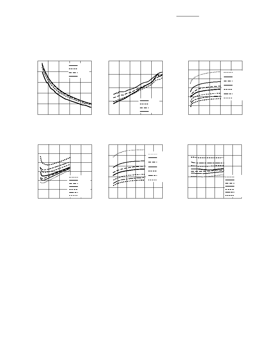
HBFP-0420 Typical Performance
0
5
10
15
25
20
0
2
4
8
6
10
ASSOCIATED GAIN
(dB)
FREQUENCY (GHz)
Figure 1. Associated Gain vs.
Frequency and Collector Current
at 2 V.
5
0
10
20
15
30
25
0
ASSOCIATED GAIN
(dB)
COLLECTOR CURRENT (mA)
Figure 2. Noise Figure vs.
Frequency and Collector Current at
2 V.
Figure 3. Associated Gain vs.
Collector Current and Frequency
at 2 V.
Figure 5. Associated Gain vs. Voltage
(V
CE
) at 5 mA.
Figure 6. Noise Figure vs. Voltage
(V
CE
) at 5 mA.
Figure 4. Noise Figure vs. Collector
Current and Frequency at 2 V.
2 mA
5 mA
10 mA
15 mA
0
0.50
1.00
3.00
1.50
2.00
NOISE FIGURE
(dB)
COLLECTOR CURRENT (mA)
2.50
0
1
2
4
5
3
6
VOLTAGE (V)
VOLTAGE (V)
0
1
2
3
4
0
2
4
8
6
10
NOISE FIGURE
(dB)
FREQUENCY (GHz)
5
10
20
15
25
2 mA
5 mA
10 mA
15 mA
0.9 GHz
1.8 GHz
2.5 GHz
3 GHz
4 GHz
5 GHz
6 GHz
0.9 GHz
1.8 GHz
2.5 GHz
3 GHz
4 GHz
5 GHz
6 GHz
0
ASSOCIATED GAIN
(dB)
0.9 GHz
1.8 GHz
2.5 GHz
3 GHz
4 GHz
5 GHz
6 GHz
0
1
2
4
5
3
6
0.5
0
1.0
2.0
1.5
2.5
NOISE FIGURE
(dB)
0.9 GHz
1.8 GHz
2.5 GHz
3 GHz
4 GHz
5 GHz
6 GHz
0
5
10
20
15
25
5
10
15
25
20