 | –≠–ª–µ–∫—Ç—Ä–æ–Ω–Ω—ã–π –∫–æ–º–ø–æ–Ω–µ–Ω—Ç: HCMS-235 | –°–∫–∞—á–∞—Ç—å:  PDF PDF  ZIP ZIP |

Agilent HCMS-235x
CMOS Extended Temperature Range
5 x 7 Alphanumeric Display
Data Sheet
Features
∑ On-Board low power CMOS IC
Integrated shift register with
constant current LED drivers
∑ Wide operating temperature range
-55∞C to +100∞C
∑ Compact glass ceramic 4
character package
Series X-Y stackable
∑ Sunlight viewable
∑ 5 x 7 LED matrix displays full
ASCII set
∑ Character height of 5.0 mm
(0.20 inch)
∑ Wide viewing angle
X Axis = ±50∞
Y Axis = ±65∞
∑ Usable in night vision lighting
applications
Typical Applications
∑ Avionics
∑ Communication systems
∑ Fire control systems
∑ Radar systems
Description
This sunlight viewable 5 x 7
LED four-character display is
contained in 12 pin dual-in-line
packages designed for
displaying alphanumeric
information. The display is
designed with on-board CMOS
integrated circuits. Two CMOS
ICs form an on-board 28-bit
serial-in/parallel-out shift
register with constant current
output LED row drivers.
Decoded column data is clocked
into the on-board shift register
for each refresh cycle. Full
character display is achieved
with external column strobing.
2
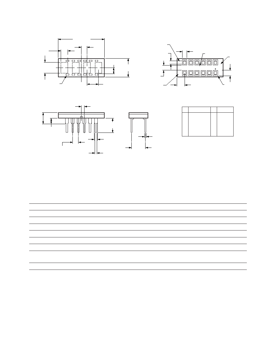
Package Dimensions
Absolute Maximum Ratings
Parameter
Value
Supply Voltage V
DD
to Ground
≠0.3 V to 7.0 V
[1]
Data Input, Data Output, V
B
≠0.3 V to V
DD
Column Input Voltage, V
COL
≠0.3 V to V
DD
Free Air Operating Temperature Range, T
A
≠55∞C to +100∞C
Storage Temperature Range, T
s
≠55∞C to +100∞C
Maximum Allowable Package Power Dissipation, P
D
[2,3]
at T
A
= 71∞C
1.31 Watts
Through-the-Wave Solder Temperature
250∞C for 3 secs. max.
1.59 mm (0.063") Below Body
ESD Protection @ 1.5 k
, 100 pF
V
Z
= 4 kV
Notes:
1. Maximum duration 2 seconds.
2. Maximum allowable power dissipation is derived from V
DD
= 5.25 V, V
B
= 2.4 V, V
COL
= 3.5 V, 20 LEDs ON per character, 20% DF.
3. HCMS-2353 derate above 71∞C at 23 mW/∞C, R
q
J-A
= 45∞C/W.
Derating based on R
qPC-A = 35∞C/W per display for printed circuit board assembly.
4
12
11
10
9
8
7
1
2
3
4
5
6
1
2
3
4.87
(0.192)
REF.
2.84
(0.112)
REF.
CL
5.00 ± 0.13
(0.197 ± 0.005)
SEE
NOTE 3
20.01
(0.790) MAX.
SEE NOTE 3
8.43
(0.332)
PIN 1 MARKED BY DOT
ON BACK OF PACKAGE
1.27 ± 0.13
(0.050 ± 0.005)
2.54
(0.100)
5.08
(0.200)
6.85
(0.270)
1.27
(0.050)
TYP.
TYP.
0.54 ± 0.08
(0.020 ± 0.003)
2.54 ± 0.13
(0.100 ± 0.005)
NON ACCUM.
TYP.
0.25 ± 0.08
(0.010 ± 0.003)
6.35 ± 0.25
(0.250 ± 0.010)
HCMS-23XX
XZ
XXYY
1.78
(0.070)
PART NUMBER
DATE CODE
2.41
(0.095)
3.56
(0.140)
2.79 ± 0.13
(0.110 ± 0.006)
1.27
(0.050)
COLOR BIN
LUMINOUS INTENSITY
CATEGORY
PIN 1
1
2
3
4
5
6
COLUMN 1
COLUMN 2
COLUMN 3
COLUMN 4
COLUMN 5
INT. CONNECT*
7
8
9
10
11
12
DATA OUT
VB
V
DD
CLOCK
GROUND
DATA IN
PIN
FUNCTION
PIN FUNCTION
* DO NOT CONNECT OR USE
NOTES:
1. DIMENSIONS IN MILLIMETERS (INCHES).
2. UNLESS OTHERWISE SPECIFIED, THE
TOLERANCE ON ALL DIMENSIONS IS
± 0.38 mm (± 0.015).
3. CHARACTERS ARE CENTERED WITH RESPECT
TO LEADS WITHIN ± 0.13 mm (± 0.005).
4. LEAD MATERIAL IS COPPER ALLOY,
SOLDER DIPPED.

3
Recommended Operating Conditions
Over Operating Range (≠55∞C to + 100∞C)
Parameter
Symbol
Min.
Typ.
Max
Units
Supply Voltage
V
DD
4.75
5.00
5.25
V
Data Out Current, Low State
I
OL
1.6
mA
Data Out Current, High State
I
OH
≠0.5
mA
Column Input Voltage
V
COL
2.75
3.0
3.5
V
Setup Time
t
SETUP
10
ns
Hold Time
t
HOLD
25
ns
Clock Pulse Width High
t
WH(CLOCK)
50
ns
Clock Pulse Width Low
t
WL(CLOCK)
50
ns
Clock High to Low Transition
t
THL
200
ns
Clock Frequency
f
CLOCK
5
MHz
Electrical Characteristics
Over Operating Range (≠55∞C to + 100∞C)
Parameter
Symbol
Test Conditions
Min
Typ.*
Max Units
Supply Current, Dynamic
[1]
I
DDD
f
CLOCK
= 5 MHz
6.2
7.8
mA
Supply Current, Static
[2]
I
DDDSoff
V
B
= 0.4 V, Data and Clock = 0.4 V
1.8
26
mA
I
DDDSon
V
B
= 2.4 V, Data and Clock = 0.4 V
2.2
6.0
Column Input Current
I
COL
V
B
= 0.4 V
10
µA
V
B
= 2.4 V
500
650
mA
Input Logic High Data, V
B
, Clock
V
IH
V
DD
= 4.75 V
2.0
V
Input Logic Low Data, V
B
, Clock
V
IL
V
DD
= 5.25 V
0.8
V
Input Current
I
I
V
DD
= 5.25 V
Data
V
I
[3]
= 2.4 V (Logic High) or
≠46
≠60
≠103
µA
Clock, V
B
V
I
[3]
= 0.4 V (Logic Low)
≠92
≠120
≠206
Data Out Voltage
V
OH
V
DD
= 4.75 V
2.4
4.2
V
I
OH
= ≠0.5 mA
I
COL
= 0 mA
V
OL
V
DD
= 5.25 V
0.2
0.4
V
I
OL
= 1.6 mA
I
COL
= 0 mA
Power Dissipation Per Package
[4]
P
D
V
DD
= 5.0 V
668
mW
V
COL
= 5.0 V
17.5% DF
V
B
= 2.4 V
15 LEDs ON per Character
Thermal Resistance
R
q
J-PIN
10
∞C/W
IC Junction-to-Pin
[5]
Leak Rate
5x10
-8
cc/sec
*All typical values specified at V
DD
= 5.0 V and T
A
= 25∞C.
Notes:
1. I
DD
Dynamic is the IC current while clocking column data through the on-board shift register at a clock frequency of 5 MHz, the display is not
illuminated.
2. I
DD
Static is the IC current after column data is loaded and not being clocked through the on-board shift register.
3. V
I
represents the input voltage to an input pin.
4. Four characters are illuminated with a typical ASCII character composed of 15 dots per character.
5. IC junction temperature T
J
(IC) = (P
D
)(R
q
J-PIN
+ R
q
PC-A
) + T
A
.

4
Switching Characteristics
Parameter
Condition
Typ. Max. Units
f
clock
CLOCK Rate
5
MHz
t
PLH
, t
PHL
C
L
= 15 pF
105
ns
Propagation Delay
R
L
= 2.4 k
CLOCK to DATA OUT
t
OFF
V
B
(0.4 V) to
4
5
µs
Display OFF
t
ON
V
B
(2.4 V) to
1
2
Display ON
Optical Characteristics at T
A
= 25∞C
High Performance Green HCMS-2353
Description
Symbol
Test Condition
Min.
Typ.*
Max.
Units
Peak Luminous Intensity per LED
[6]
I
vPEAK
V
DD
= 5.0 V
2400
3000
µcd
(Character Average)
V
COL
= 5.0 V
V
B
= 2.4 V
T
i
= 25∞C
[7]
Dominant Wavelength
[8,9]
l
d
574
nm
Peak Wavelength
l
PEAK
568
nm
Yellow HCMS-2351
*All typical values specified at V
DD
= 5.0 V and T
A
= 25∞C unless otherwise noted.
Notes:
6. These LED displays are categorized for luminous intensity, with the intensity category designated by a letter code on the back of the package.
7. T
i
refers to the initial case temperature of the display immediately prior to the light measurement.
8. Dominant wavelength,
l
d
, is derived from the CIE Chromaticity Diagram, and represents the single wavelength which defines the color of the device.
9. Categorized for color with the color category designated by a number on the back of the package.
t
WH
t
THL
t
WL
1/f
CLOCK
t
HOLD
t
SETUP
t
PLH
, t
PHL
t
OFF
t
ON
V
IH
V
IL
V
B
V
OH
V
OL
2.4 V
0.4 V
2.0 V
0.8 V
V
IH
V
IL
2.0 V
0.8 V
V
IH
V
IL
2.0 V
0.8 V
CLOCK
DATA IN
DATA OUT
90%
10%
ON (ILLUMINATED)
OFF (NOT ILLUMINATED)
DISPLAY
Description
Symbol
Test Condition
Min
Typ.*
Max.
Units
Peak Luminous Intensity per
LED
[6]
(Character Average)
I
vPEAK
V
DD
= 5.0V
V
COL
= 5.0 V
V
B
= 2.4V
Ti = 25∞C
[7]
1600
2400
µcd
Dominant Wavelength
[8,9]
d
585
nm
Peak Wavelength
PEAK
583
nm
5
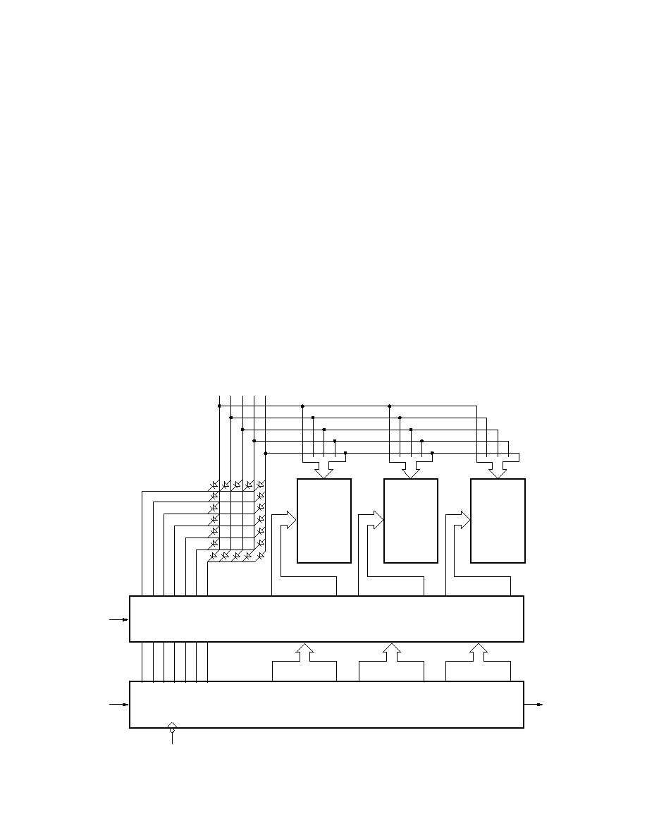
Electrical Description
The display contains four 5 x 7
LED dot matrix characters and
two CMOS integrated circuits,
as shown in Figure 1. The two
CMOS integrated circuits form
an on-board 28 bit serial-in/
parallel-out shift register that
will accept standard TTL logic
levels. The Data Input, pin 12,
is connected to bit position 1
and the Data Output, pin 7, is
connected to bit position 28.
The shift register outputs
control constant current sinking
LED row drivers. A logic 1
stored in the shift register
enables the corresponding LED
row driver and a logic 0 stored
in the shift register disables the
corresponding LED row driver.
The electrical configuration of
these CMOS IC alphanumeric
displays allows for an effective
interface to a display controller
circuit that supplies decoded
character information. The row
data for a given column (one 7
bit byte per character) is loaded
(bit serial) into the on-board 28
bit shift register with high to
low transitions of the Clock
input. To load decoded
character information into the
display, column data for
character 4 is loaded first and
the column data for character 1
is loaded last in the following
manner. The 7 data bits for
column 1, character 4, are
loaded into the on-board shift
register. Next, the 7 data bits
for column 1, character 3, are
loaded into the shift register,
shifting the character 4 data
over one character position.
This process is repeated for the
other two characters until all 28
bits of column data (four 7 bit
bytes of character column data)
are loaded into the on-board
shift register. Then the column
1 input, V
COL
pin 1, is
energized to illuminate column
1 in all four characters. This
process is repeated for columns
2, 3, 4 and 5. All V
COL
inputs
should be at logic low to insure
the display is off when loading
data. The display will be
blanked when the blanking
input V
B
, pin 8, is at logic low
regardless of the outputs of the
shift register or whether one of
the V
COL
inputs is energized.
Refer to Application Note 1016
for drive circuit information.
Figure 1. Display block diagram.
ROWS 1-7
CONSTANT CURRENT SINKING LED DRIVERS
COLUMN DRIVE INPUTS
COLUMN
ROWS
1
LED
MATRIX
2
ROWS 8-14
CLOCK
ROWS 1-7
LED
MATRIX
3
ROWS 15-21
ROWS 1-7
LED
MATRIX
4
ROWS 22-28
2 3 4 5 6 7
1 2 3 4 5
1
2
3
4
5
6 7
28-BIT SIPO SHIFT REGISTER
SERIAL
DATA
OUTPUT
SERIAL
DATA
INPUT
BLANKING
CONTROL, V
B