 | –≠–ª–µ–∫—Ç—Ä–æ–Ω–Ω—ã–π –∫–æ–º–ø–æ–Ω–µ–Ω—Ç: HCPL-063L | –°–∫–∞—á–∞—Ç—å:  PDF PDF  ZIP ZIP |
Document Outline
- ˛ˇg,0«0¸0ø0÷0√0Ø0kï¢0W0f
- ˛ˇvÓk!
- ˛ˇ0‚0«0ÎujS˜R%}"_�
- ˛ˇ0π0Î0¸0€0¸0Î
- ˛ˇ0µ0¸0’0ß0π0Þ0¶0Û0»
- ˛ˇóbvzQI0¿0§0™0¸0…
- ˛ˇ
- ˛ˇ0¢0Î0’0°0Ÿ0√0»àhy:Vh
- ˛ˇ0’0©0»0´0◊0È
- ˛ˇQI[f_�0®0Û0≥0¸0¿
- ˛ˇçdY�}⁄ê�O·} [P
- ˛ˇQI0’0°0§0–0‚0∏0Â0¸0Î0˚rit�\d
- ˛ˇå©XÚ}≤
6 - 104
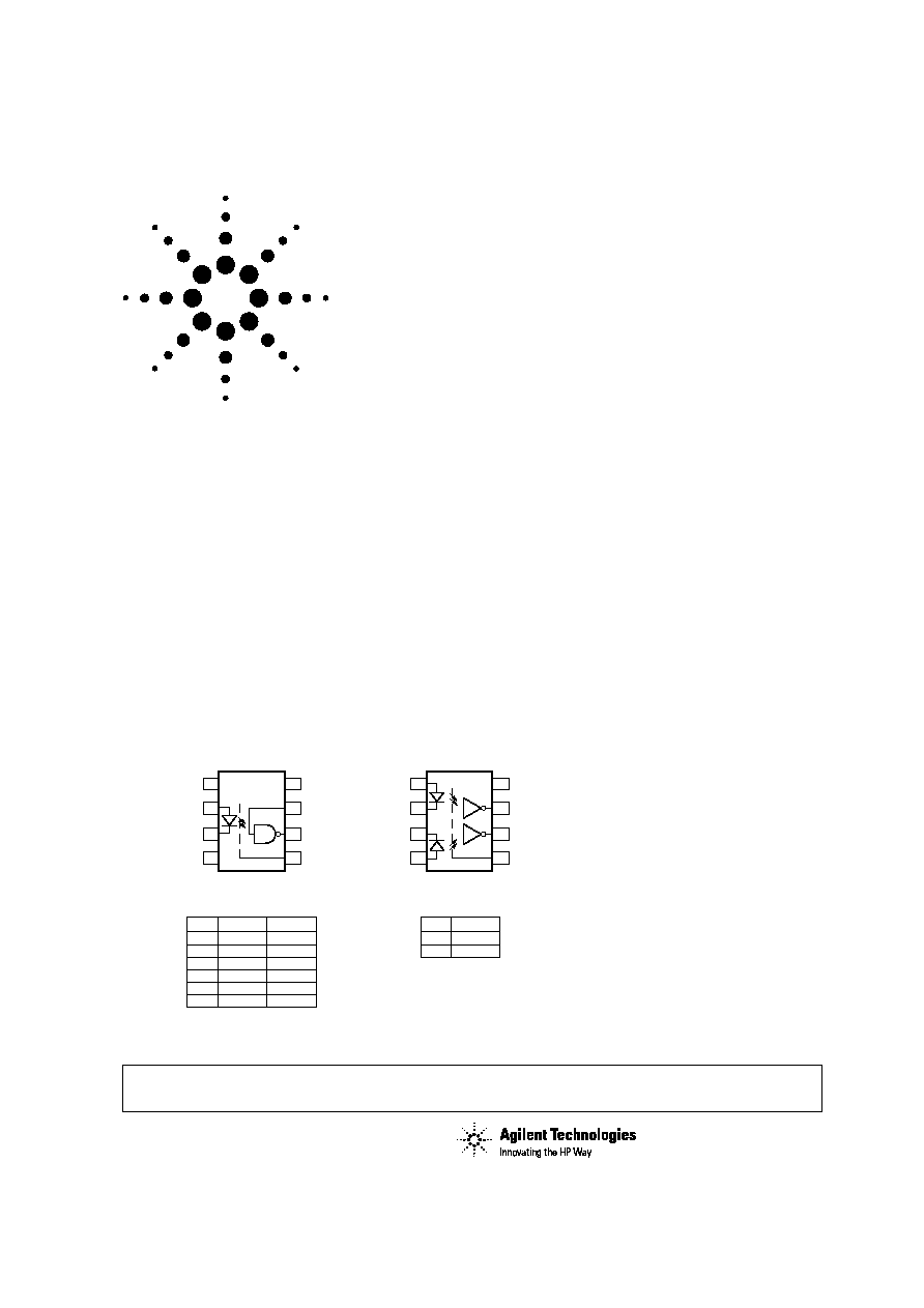
Description
The HCPL-260L/060L/263L/063L
are optically coupled gates that
combine a GaAsP light emitting
diode and an integrated high gain
photo detector. An enable input
allows the detector to be strobed.
The output of the detector IC is an
open collector Schottky-clamped
transistor. The internal shield
provides a guaranteed common
mode transient immunity
specification of 15 kV/
µs.
Agilent HCPL-260L/ 060L/263L/063L
High Speed LVTTL Compatible
3.3 Volt Optocouplers
Data Sheet
Features
∑ Low power consumption
∑ 15 kV/
µs minimum Common Mode
Rejection (CMR) at V
CM
= 50 V
∑ High speed: 15 MBd typical
∑ LVTTL/LVCMOS compatible
∑ Low input current capability:
5 mA
∑ Guaranteed AC and DC performance
over temperature: ≠40∞C to +85∞C
∑ Available in 8-pin DIP, SOIC-8
∑ Strobable output (single channel
products only)
∑ Safety approvals; UL, CSA, VDE
(pending)
Applications
∑ Isolated line receiver
∑ Computer-peripheral interfaces
∑ Microprocessor system interfaces
∑ Digital isolation for A/D, D/A
conversion
∑ Switching power supply
∑ Instrument input/output isolation
∑ Ground loop elimination
∑ Pulse transformer replacement
∑ Field buses
Functional Diagram
This unique design provides
maximum AC and DC circuit
isolation while achieving
LVTTL/LVCMOS compatibility.
The optocoupler AC and DC
operational parameters are
guaranteed from ≠40∞C to +85∞C
allowing trouble-free system
performance.
A 0.1
µF bypass capacitor must be connected between pins 5 and 8.
CAUTION: It is advised that normal static precautions be taken in handling and assembly of this component to prevent
damage and/or degradation which may be induced by ESD.
1
2
3
4
8
7
6
5
CATHODE
ANODE
GND
V
VCC
O
1
2
3
4
8
7
6
5
ANODE 2
CATHODE 2
CATHODE 1
ANODE 1
GND
V
VCC
O2
VE
VO1
HCPL-260L/060L
HCPL-263L/063L
NC
NC
LED
ON
OFF
ON
OFF
ON
OFF
ENABLE
H
H
L
L
NC
NC
OUTPUT
L
H
H
H
L
H
TRUTH TABLE
(POSITIVE LOGIC)
LED
ON
OFF
OUTPUT
L
H
TRUTH TABLE
(POSITIVE LOGIC)
SHIELD
SHIELD
6 - 104
6104-117(PDF)
01.5.24, 4:23 PM
Page 104
Adobe PageMaker 6.0J/PPC
6 - 105
These optocouplers are suitable
for high speed logic interfacing,
input/output buffering, as line
receivers in environments that
conventional line receivers
cannot tolerate and are
recommended for use in
extremely high ground or induced
noise environments.
These optocouplers are available
in an 8-pin DIP and industry
standard SO-8 package. The part
numbers are as follows:
8-pin DIP
SO-8 Package
HCPL-260L
HCPL-060L
HCPL-263L
HCPL-063L
Ordering Information
Specify Part Number followed by Option Number (if desired).
Example:
HCPL-260L #XXX
060 = VDE 0884 V
IORM
= 630 Vpeak Option
500 = Tape and Reel Packaging Option
Option data sheets available. Contact Agilent sales representative or
authorized distributor for information.
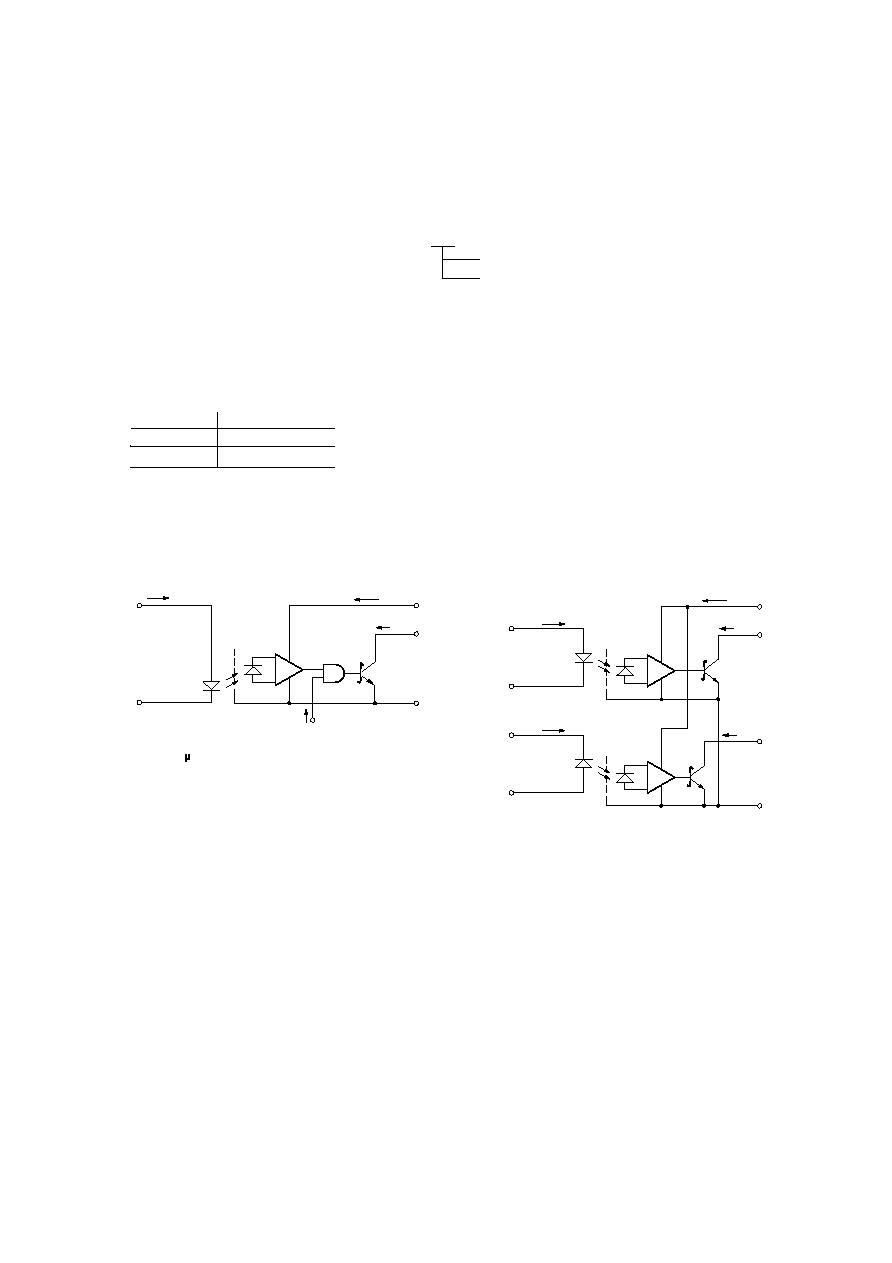
Schematic
SHIELD
8
6
5
2+
3
VF
USE OF A 0.1 F BYPASS CAPACITOR CONNECTED
BETWEEN PINS 5 AND 8 IS RECOMMENDED (SEE NOTE 5).
≠
IF
ICC
VCC
VO
GND
IO
VE
IE
7
HCPL-260L/060L
SHIELD
8
7
+
2
VF1
≠
IF1
ICC
VCC
VO1
IO1
1
SHIELD
6
5
≠
4
VF2
+
IF2
VO2
GND
IO2
3
HCPL-263L/063L
6104-117(PDF)
01.5.24, 4:23 PM
Page 105
Adobe PageMaker 6.0J/PPC
6 - 106
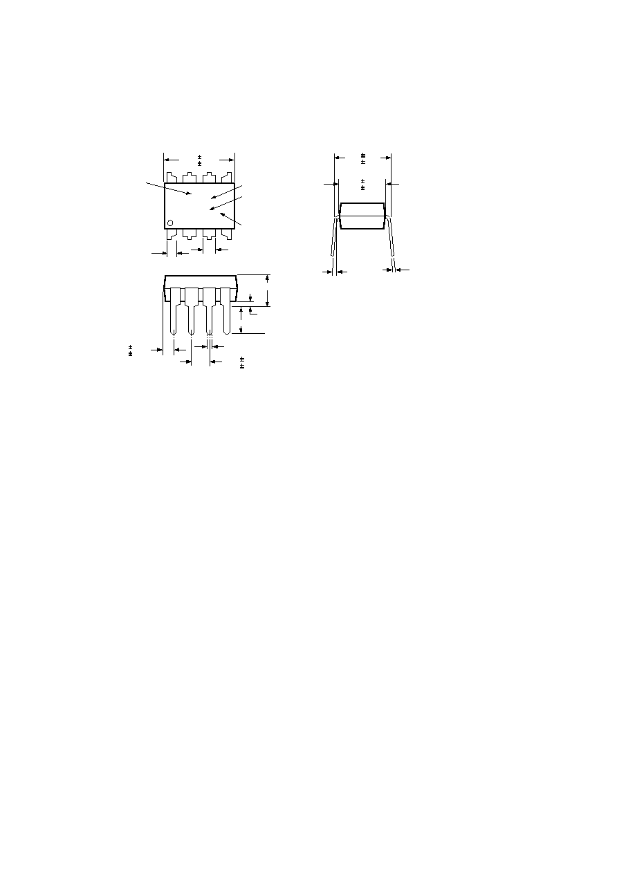
Package Outline Drawings
8-Pin DIP Package
1.080
± 0.320
(0.043
± 0.013)
2.54
± 0.25
(0.100
± 0.010)
0.51 (0.020) MIN.
0.65 (0.025) MAX.
4.70 (0.185) MAX.
2.92 (0.115) MIN.
5
∞ TYP.
0.254
+ 0.076
- 0.051
(0.010
+ 0.003)
- 0.002)
7.62
± 0.25
(0.300
± 0.010)
6.35
± 0.25
(0.250
± 0.010)
9.65
± 0.25
(0.380
± 0.010)
1.78 (0.070) MAX.
1.19 (0.047) MAX.
A XXXXZ
YYWW
DATE CODE
DIMENSIONS IN MILLIMETERS AND (INCHES).
5
6
7
8
4
3
2
1
OPTION CODE*
UL
RECOGNITION
UR
TYPE NUMBER
*MARKING CODE LETTER FOR OPTION NUMBERS
"L" = OPTION 020
"V" = OPTION 060
OPTION NUMBERS 300 AND 500 NOT MARKED.
6104-117(PDF)
01.5.24, 4:23 PM
Page 106
Adobe PageMaker 6.0J/PPC
6 - 107
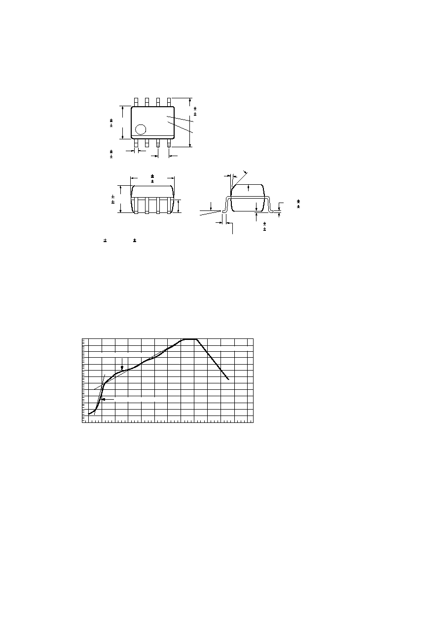
Small Outline SO-8 Package
Solder Reflow Temperature Profile
(Surface Mount Option Parts)
Regulatory Information
The HCPL-260L/060L/263L/063L
are pending by the following
organizations:
UL
Approval (pending) under UL
1577, Component Recognition
Program, File E55361.
CSA
Approval (pending) under CSA
Component Acceptance Notice
#5, File CA 88324.
VDE
Approval (pending) according to
VDE 0884/06.92.
XXX
YWW
8
7
6
5
4
3
2
5.994
± 0.203
(0.236
± 0.008)
3.937
± 0.127
(0.155
± 0.005)
0.406
± 0.076
(0.016
± 0.003)
1.270
(0.050)
BSG
5.080
± 0.127
(0.200
± 0.005)
3.175
± 0.127
(0.125
± 0.005)
1.524
(0.060)
45
∞ X
0.432
(0.017)
0.228
± 0.025
(0.009
± 0.001)
TYPE NUMBER
(LAST 3 DIGITS)
DATE CODE
0.305
(0.012)
MIN.
TOTAL PACKAGE LENGTH (INCLUSIVE OF MOLD FLASH)
5.207
± 0.254 (0.205 ± 0.010)
DIMENSIONS IN MILLIMETERS (INCHES).
LEAD COPLANARITY = 0.10 mm (0.004 INCHES) MAX.
0.203
± 0.102
(0.008
± 0.004)
7
∞
PIN ONE
0 ~ 7
∞
*
*
240
T = 115∞C, 0.3∞C/SEC
0
T = 100∞C, 1.5∞C/SEC
T = 145∞C, 1∞C/SEC
TIME ≠ MINUTES
TEMPERA
TURE
≠
∞
C
220
200
180
160
140
120
100
80
60
40
20
0
260
1
2
3
4
5
6
7
8
9
10
11
12
NOTE: USE OF NON-CHLORINE ACTIVATED FLUXES IS HIGHLY RECOMMENDED.
1
6104-117(PDF)
01.5.24, 4:23 PM
Page 107
Adobe PageMaker 6.0J/PPC

6 - 108
Insulation and Safety Related Specifications
8-Pin DIP
(300 Mil)
SO-8
Parameter
Symbol
Value
Value
Units
Conditions
Minimum External Air
L (101)
7.1
4.9
mm
Measured from input terminals to output
Gap (External Clearance)
terminals, shortest distance through air.
Minimum External Tracking
L (102)
7.4
4.8
mm
Measured from input terminals to output
(External Creepage)
terminals, shortest distance path along body.
Minimum Internal Plastic
0.08
0.08
mm
Through insulation distance, conductor to
Gap (Internal Clearance)
conductor, usually the direct distance
between the photoemitter and photodetector
inside the optocoupler cavity.
Minimum Internal Tracking
NA
NA
mm
Measured from input terminals to output
(Internal Creepage)
terminals, along internal cavity.
Tracking Resistance
CTI
200
200
Volts
DIN IEC 112/VDE 0303 Part 1
(Comparative Tracking
Index)
Isolation Group
IIIa
IIIa
Material Group (DIN VDE 0110, 1/89, Table 1)
VDE 0884 Insulation Related Characteristics
Description
Symbol
Characteristic
Units
Installation classification per DIN VDE 0110/1.89, Table 1
for rated mains voltage
300 V rms
I-IV
for rated mains voltage
450 V rms
I-III
Climatic Classification
55/85/21
Pollution Degree (DIN VDE 0110/1.89)
2
Maximum Working Insulation Voltage
V
IORM
630
V
peak
Input to Output Test Voltage, Method b*
V
IORM
x 1.875 = V
PR
, 100% Production Test with t
m
= 1 sec,
V
PR
1181
V
peak
Partial Discharge < 5 pC
Input to Output Test Voltage, Method a*
V
IORM
x 1.5 = V
PR
, Type and Sample Test,
V
PR
945
V
peak
t
m
= 60 sec, Partial Discharge < 5 pC
Highest Allowable Overvoltage*
V
IOTM
6000
V
peak
(Transient Overvoltage, t
ini
= 10 sec)
Safety Limiting Values
(Maximum values allowed in the event of a failure,
also see Figure 16, Thermal Derating curve.)
Case Temperature
T
S
175
∞C
Input Current
I
S,INPUT
230
mA
Output Power
P
S,OUTPUT
600
mW
Insulation Resistance at T
S
, V
IO
= 500 V
R
S
10
9
*Refer to the front of the optocoupler section of the current catalog, under Product Safety Regulations section (VDE 0884), for a detailed description.
Note: Isolation characteristics are guaranteed only within the safety maximum ratings which must be ensured by protective circuits in application.
6104-117(PDF)
01.5.24, 4:23 PM
Page 108
Adobe PageMaker 6.0J/PPC