 | –≠–ª–µ–∫—Ç—Ä–æ–Ω–Ω—ã–π –∫–æ–º–ø–æ–Ω–µ–Ω—Ç: HCPL-0738 | –°–∫–∞—á–∞—Ç—å:  PDF PDF  ZIP ZIP |

Description
The HCPL-0738 is a dual-channel
15 MBd CMOS optocoupler in
SOIC-8 package. The HCPL-0738
optocoupler utilizes the latest CMOS
IC technology to achieve out-
standing performance with very low
power consumption. Basic building
blocks of HCPL-0738 are high
speed LEDs and CMOS detector ICs.
Agilent HCPL-0738
High Speed CMOS Optocoupler
Data Sheet
Features
∑ 15 ns typical pulse width
distortion
∑ 40 ns maximum prop. delay skew
∑ 20 ns typical prop. delay
∑ High speed: 15 MBd
∑ + 5 V CMOS compatibility
∑ 10 kV/
µ
S minimum common mode
rejection
∑ ≠40 to 100∞C temperature range
∑ Safety and regulatory approvals
≠ UL recognized (2500 V rms for
1 minute per UL 1577)
≠ CSA component acceptance
notice #5.
≠ VDE 0884 (TUV) approved for
HCPL-0738 Option 060
Applications
∑ PDP (plasma display panel)
∑ Digital field bus isolation:
DeviceNet, SDS, Profibus
∑ Multiplexed data transmission
∑ Computer peripheral interface
∑ Microprocessor system interface
∑ DC/DC converter
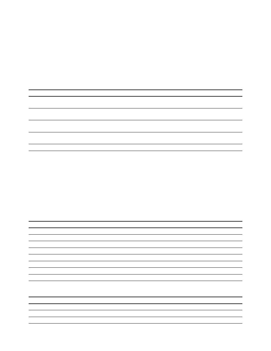
CAUTION: It is advised that normal static precautions be taken in handling and assembly of this
component to prevent damage and/or degradation which may be induced by ESD.
Truth Table
LED
V
O
, Output
OFF
H
ON
L
Note: A 0.1
µ
F bypass capacitor must be
connected between pins 5 and 8.
Functional Diagram
Agilent also offers the same
performance in the single channel
version, HCPL-0708. Each
detector incorporates an
integrated photodiode, a high
speed transimpedance amplifier,
and a voltage comparator with an
output driver.
8
7
6
1
3
5
2
4
ANODE 1
CATHODE 1
CATHODE 2
ANODE 2
VDD
VO 2
GND
VO 1
2
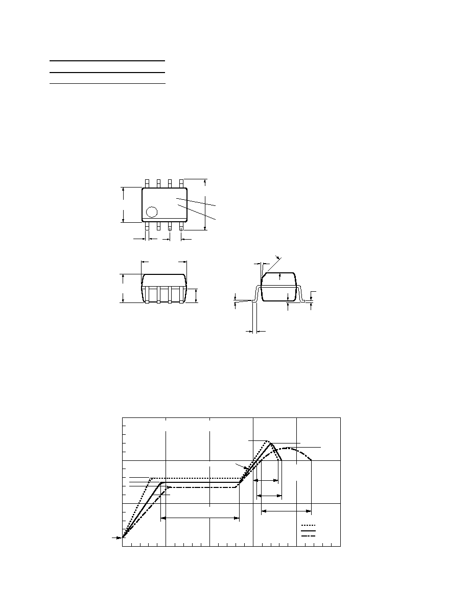
Package Outline Drawing
HCPL-0738 Outline Drawing (Small Outline SO-8 Package)
Ordering Information
Specify Part Number followed by
Option Number (if desired).
Example
HCPL-0738 -060 = VDE0884
Option
HCPL-0738 -500 = Tape and
Reel Packaging Option
No Option Code contains 100
units per tube. Option 500
contains 1500 units per reel.
Option data sheets available.
Contact Agilent Technologies
sales representative or authorized
distributor.
Selection Guide
Small Outline SO-8
HCPL-0738
Solder Reflow Temperature Profile
0
TIME (SECONDS)
TEMPERATURE (∞C)
200
100
50
150
100
200
250
300
0
30
SEC.
50 SEC.
30
SEC.
160∞C
140∞C
150∞C
PEAK
TEMP.
245∞C
PEAK
TEMP.
240∞C
PEAK
TEMP.
230∞C
SOLDERING
TIME
200∞C
PREHEATING TIME
150∞C, 90 + 30 SEC.
2.5∞C ± 0.5∞C/SEC.
3∞C + 1∞C/≠0.5∞C
TIGHT
TYPICAL
LOOSE
ROOM
TEMPERATURE
PREHEATING RATE 3∞C + 1∞C/≠0.5∞C/SEC.
REFLOW HEATING RATE 2.5∞C ± 0.5∞C/SEC.
XXX
YWW
8
7
6
5
4
3
2
1
PIN
ONE
7∞
5.994 ± 0.203
(0.236 ± 0.008)
3.937 ± 0.127
(0.155 ± 0.005)
0.405 ± 0.076
(0.015 ± 0.003)
1.270
(0.050)
BSG
*5.080 ± 0.127
(0.205 ± 0.005)
3.175 ± 0.127
(0.125 ± 0.005)
1.524
(0.060)
45∞ x 0.432
(0.017)
0.228 ± 0.025
(0.009 ± 0.001)
0.202 ± 0.102
(0.008 ± 0.004)
TYPE NUMBER
(LAST 3 DIGITS)
DATE CODE
*TOTAL PACKAGE LENGTH (INCLUSIVE OF MOLD FLASH)
5.207 ± 0.254 (0.205 ± 0.010)
DIMENSIONS IN MILLIMETERS AND (INCHES).
LEAD COPLANARITY = 0.10 mm (0.004 INCHES) MAX.
0.305
(0.012)
MIN.
0 - 7∞
3
All Agilent data sheets report the
creepage and clearance inherent
to the optocoupler component
itself. These dimensions are
needed as a starting point for the
equipment designer when deter-
mining the circuit insulation re-
quirements. However, once
mounted on a printed circuit
Regulatory Information
The HCPL-0738 has been
approved by the following
organizations:
UL
Recognized under UL 1577,
component recognition program,
File E55361.
CSA
Approved under CSA Component
Acceptance Notice #5, File
CA88324.
TUV
Approved according to
VDE 0884/06.92, Certificate
R9650938.
board, minimum creepage and
clearance requirements must be
met as specified for individual
equipment standards. For creep-
age, the shortest distance path
along the surface of a printed
circuit board between the solder
fillets of the input and output
leads must be considered. There
are recommended techniques
such as grooves and ribs which
may be used on a printed circuit
board to achieve desired creep-
age and clearances. Creepage and
clearance distances will also
change depending on factors
such as pollution degree and
insulation level.
Insulation and Safety Related Specifications (approval pending)
Parameter
Symbol
Value
Units
Conditions
Minimum External Air Gap
L(I01)
4.9
mm
Measured from input terminals to output terminals,
(Clearance)
shortest distance through air.
Minimum External Tracking
L(I02)
4.8
mm
Measured from input terminals to output terminals,
(Creepage)
shortest distance path along body.
Minimum Internal Plastic Gap
0.08
mm
Insulation thickness between emitter and detector; also
(Internal Clearance)
known as distance through insulation.
Tracking Resistance
CTI
175
Volts
DIN IEC 112/VDE 0303 Part 1
(Comparative Tracking Index)
Isolation Group
IIIa
Material Group (DIN VDE 0110, 1/89, Table 1)
Absolute Maximum Ratings
Parameter
Symbol
Minimum
Maximum
Units
Storage Temperature
T
S
≠55
125
∞C
Ambient Operating Temperature
T
A
≠40
100
∞C
Supply Voltage
V
DD
0
6.0
Volts
Output Voltage
V
O
≠0.5
V
DD
+ 0.5
Volts
Average Forward Input Current
I
F
--
20
mA
Average Output Current
I
O
--
2
mA
Lead Solder Temperature
260∞C for 10 seconds, 1.6 mm below seating plane
Solder Reflow Temperature Profile
See Solder Reflow Thermal Profile section
Recommended Operating Conditions
Parameter
Symbol
Minimum
Maximum
Units
Ambient Operating Temperature
T
A
≠40
100
∞C
Supply Voltages
V
DD
4.5
5.5
V
Input Current (ON)
I
F
10
16
mA

4
Switching Specifications
Over recommended temperature (T
A
= ≠40∞C to +100∞C) and 4.5 V
V
DD
5.5 V.
All typical specifications are at T
A
= 25∞C, V
DD
= +5 V.
Parameter
Symbol
Min.
Typ.
Max.
Units
Test Conditions
Fig.
Notes
Propagation Delay Time
t
PHL
20
35
60
ns
I
F
= 12 mA, C
L
= 15 pF
5
1
to Logic Low Output
CMOS Signal Levels
Propagation Delay Time
t
PLH
11
20
60
ns
I
F
= 12 mA, C
L
= 15 pF
5
1
to Logic High Output
CMOS Signal Levels
Pulse Width
PW
100
ns
Pulse Width Distortion
|PWD|
0
15
30
ns
I
F
= 12 mA, C
L
= 15 pF
5
2
CMOS Signal Levels
Propagation Delay Skew
t
PSK
40
ns
I
F
= 12 mA, C
L
= 15 pF
3
CMOS Signal Levels
Output Rise Time
t
R
20
ns
I
F
= 0 mA, C
L
= 15 pF
(10% ≠ 90%)
CMOS Signal Levels
Output Fall Time
t
F
25
ns
I
F
= 12 mA, C
L
= 15 pF
(90% ≠ 10%)
CMOS Signal Levels
Common Mode Transient
|CM
H
|
10
15
kV/
µ
S
V
CM
= 1000 V, T
A
= 25∞C,
4
Immunity at Logic High Output
I
F
= 0 mA
Common Mode Transient
|CM
L
|
10
15
kV/
µ
S
V
CM
= 1000 V, T
A
= 25∞C,
5
Immunity at Logic Low Output
I
F
= 12 mA
Electrical Specifications
Over recommended temperature (T
A
= ≠40∞C to +100∞C) and 4.5 V
V
DD
5.5 V.
All typical specifications are at T
A
= 25∞C, V
DD
= +5 V.
Parameter
Symbol
Min.
Typ.
Max.
Units
Test Conditions
Fig.
Notes
Input Forward Voltage
V
F
1.3
1.5
1.8
V
I
F
= 12 mA
1
Input Reverse Breakdown
BV
R
5
V
I
R
= 10
µ
A
Voltage
Logic High Output Voltage
V
OH
4.0
5
V
I
F
= 0, I
O
= ≠20
µ
A
Logic Low Output Voltage
V
OL
0.01
0.1
V
I
F
= 12 mA, I
O
= 20
µ
A
Input Threshold Current
I
TH
4.5
8.2
mA
I
OL
= 20
µ
A
2
Logic Low Output Supply
I
DDL
10
18.0
mA
I
F
= 12 mA
4
Current
Logic High Output Supply
I
DDH
8
15.0
mA
I
F
= 0 mA
3
Current
5
Package Characteristics
All typicals at T
A
= 25∞C.
Parameter
Symbol
Min.
Typ.
Max.
Units
Test Conditions
Input-Output Insulation
I
I-O
1
µ
A
45% RH, t = 5 s
V
I-O
= 3 kV DC,
T
A
= 25∞C
Input-Output Momentary
V
ISO
2500
V rms
RH
50%, t = 1 min.,
Withstand Voltage
T
A
= 25∞C
Input-Output Resistance
R
I-O
10
12
V
I-O
= 500 V DC
Input-Output Capacitance
C
I-O
0.6
pF
f = 1 MHz, T
A
= 25∞C
Notes:
1. t
PHL
propagation delay is measured from the 50% level on the rising edge of the input pulse to the 2.5 V level of the falling edge of the V
O
signal.
t
PLH
propagation delay is measured from the 50% level on the falling edge of the input pulse to the 2.5 V level of the rising edge of the V
O
signal.
2. PWD is defined as |t
PHL
- t
PLH
|.
3. t
PSK
is equal to the magnitude of the worst case difference in t
PHL
and/or t
PLH
that will be seen between units at any given temperature within the
recommended operating conditions.
4. CM
H
is the maximum tolerable rate of rise of the common mode voltage to assure that the output will remain in a high logic state.
5. CM
L
is the maximum tolerable rate of fall of the common mode voltage to assure that the output will remain in a low logic state.
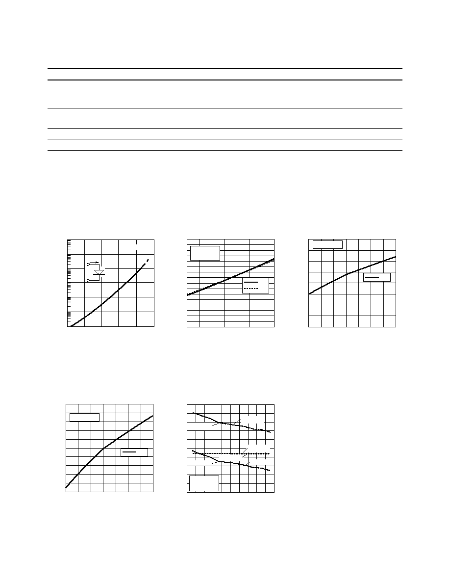
Figure 1. Typical input diode forward
characteristic.
Figure 2. Typical input threshold current vs.
temperature.
Figure 3. Typical logic high O/P supply
current vs. temperature.
Figure 4. Typical logic low O/P supply
current vs. temperature.
Figure 5. Typical switching speed vs. pulse
input current.
VF ≠ FORWARD VOLTAGE ≠ V
100
10
0.1
0.01
1.1
1.2
1.3
1.4
I F
≠ FORWARD CURRENT ≠ mA
1.6
1.5
1.0
0.001
1000
IF
VF
+
TA = 25∞C
≠
I th
≠ INPUT THRESHOLD CURRENT ≠ mA
-40
0
TA ≠ TEMPERATURE ≠ ∞C
100
7
1
60
0
20
8
5
3
4
Ith1
Ith2
-20
40
80
2
6
VDD = 5.0 V
IOL = 20 µA
tp ≠ PROPAGATION DELAY ≠ ns
5
0
IF ≠ PULSE INPUT CURRENT ≠ mA
14
45
10
11
7
9
50
30
20
25
5
40
6
8
10
12 13
15
35
VDD = 5.0 V
TA = 25 ∞C
Tphl CH 1
Tphl CH 2
Tplh CH 2
PWD CH 2
PWD CH 1
Tplh CH 1
-40
TA ≠ TEMPERATURE ≠ ∞C
100
60
0
20
Iddh
-20
40
80
I DDH
≠ LOGIC HIGH OUTPUT SUPPLY CURRENT ≠ mA
6.0
9.5
7.0
10.0
8.5
7.5
8.0
6.5
9.0
VDD = 5.0 V
-40
TA ≠ TEMPERATURE ≠ ∞C
100
60
0
20
Iddl
-20
40
80
9.6
11.4
10.0
11.6
10.8
10.4
10.6
9.8
11.2
I DDL
≠ LOGIC LOW SUPPLY CURRENT ≠ mA
11.0
10.2
VDD = 5.0 V