1-402
High Speed CMOS
Optocouplers
Technical Data
Features
� 1
�
m CMOS IC Technology
� Compatibility with All +5 V
CMOS and TTL Logic
Families
� No External Components
Required for Logic Interface
� High Speed: 15 MBd
(HCPL-7100) and 50 MBd
(HCPL-7101) Guaranteed
� Low Power Consumption
� Safety Approvals
UL 1577 (3750 Vac/1 Min)
VDE 0884 (V
IORM
= 848
V
peak
)
CSA
� 3-State Output
� 3750 Vac/1 Minute Dielectric
Withstand
� High Common Mode
Transient Immunity
Applications
� Multiplexed Data
Transmission
� Computer-Peripheral
Interface
� Microprocessor System
Interface
� Digital Isolation for A/D,
D/A Conversion
� Instrument Input/Output
Isolation
� Motor Control
� Power Inverter
Description
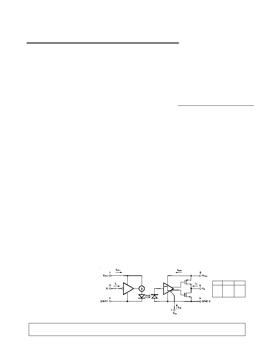
The HCPL-7100/7101 optocoup-
ler combines the latest CMOS IC
technology, a new high-speed
high-efficiency AlGaAs LED, and
an optimized light coupling system
to achieve outstanding perfor-
mance with very low power
consumption. It requires only two
bypass capacitors for complete
CMOS/TTL compatibility.
Basic building blocks of the
HCPL-7100/7101 are a CMOS
LED driver IC, an AlGaAs LED,
and a CMOS detector IC. A CMOS
or TTL logic input signal controls
the LED driver IC which supplies
current to the LED. The detector
IC incorporates an integrated
photodiode, a high-speed trans-
impedance amplifier and a voltage
comparator with hysteresis. The
3-state output is CMOS and TTL
compatible and is controlled by
the output enable pin, V
OE
.
The HCPL-7100/7101 consumes
very little power, due to the
CMOS IC technology and the light
coupling system. The entire
optocoupler typically uses only 10
mA of supply current, including
the LED current.
World-wide safety approval and
3750 Vac/1 minute dielectric with-
stand is achieved with our
patented "light-pipe" optocoupler
packaging technology.
The HCPL-7100/7101 provides he
user with an easy-to-use CMOS or
TTL compatible optocoupler
ideally suited for a variety of
applications where high speed
and low power consumption are
desired.
HCPL-7100
HCPL-7101
Schematic
CAUTION: It is advised that normal static precautions be taken in handling and assembly of this component to
prevent damage and/or degradation which may be induced by ESD.
H
TRUTH TABLE
(POSITIVE LOGIC)
INPUT
ENABLE
OUTPUT
H
H
Z
L
H
Z
H
L
H
L
L
L
5965-3578E
1-403
Ordering Information
HCPL-710x
0 = 15 MBd Minimum Data Rate
1 = 50 MBd Minimum Data Rate
Option yyy
300 = Gull Wing Surface Mount Lead Option
500 = Tape/Reel Package Option (1 k min.)
Option data sheets available. Contact your Hewlett-Packard sales representative or authorized distributor for
information.
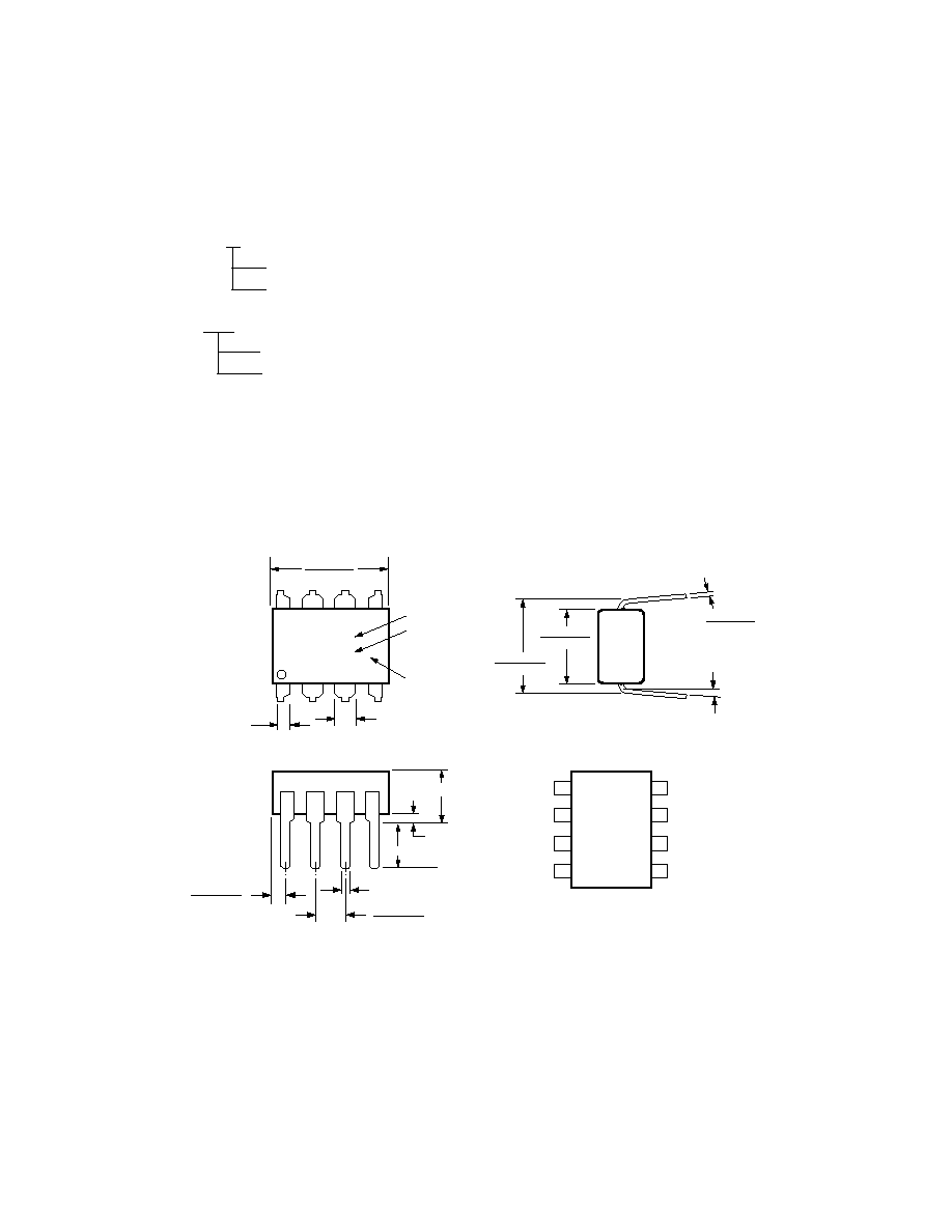
Package Outline Drawings
Standard DIP Package
9.40 (0.370)
9.90 (0.390)
1.78 (0.070) MAX.
1.19 (0.047) MAX.
HP XXXX
YYWW
DATE CODE
0.76 (0.030)
1.40 (0.055)
2.28 (0.090)
2.80 (0.110)
0.51 (0.020) MIN.
0.65 (0.025) MAX.
4.70 (0.185) MAX.
2.92 (0.115) MIN.
* PIN 3 IS THE ANODE OF THE INTERNAL LED AND
MUST BE LEFT UNCONNECTED FOR GUARANTEED
DATA SHEET PERFORMANCE.
DIMENSIONS IN MILLIMETERS AND (INCHES).
5
6
7
8
4
3
2
1
0.20 (0.008)
0.33 (0.013)
6.10 (0.240)
6.60 (0.260)
5� TYP.
7.36 (0.290)
7.88 (0.310)
1
2
3
4
8
7
6
5
GND1
VDD1
VI
*
GND2
VDD2
VOE
VO
PIN ONE
TYPE NUMBER
UL
RECOGNITION
UR
* PIN 3 IS THE ANODE OF THE INTERNAL LED AND
MUST BE LEFT UNCONNECTED FOR GUARANTEED
DATA SHEET PERFORMANCE.
DIMENSIONS IN MILLIMETERS AND (INCHES).

1-404
*Refer to Option 300 data sheet for more information.
0.635 � 0.25
(0.025 � 0.010)
12� NOM.
0.20 (0.008)
0.33 (0.013)
9.65 � 0.25
(0.380 � 0.010)
0.51 � 0.130
(0.020 � 0.005)
7.62 � 0.25
(0.300 � 0.010)
5
6
7
8
4
3
2
1
9.65 � 0.25
(0.380 � 0.010)
6.350 � 0.25
(0.250 � 0.010)
1.02 (0.040)
1.19 (0.047)
1.19 (0.047)
1.78 (0.070)
9.65 � 0.25
(0.380 � 0.010)
4.83
(0.190)
TYP.
0.380 (0.015)
0.635 (0.025)
PIN LOCATION (FOR REFERENCE ONLY)
1.080 � 0.320
(0.043 � 0.013)
4.19
(0.165)
MAX.
1.780
(0.070)
MAX.
1.19
(0.047)
MAX.
2.540
(0.100)
BSC
DIMENSIONS IN MILLIMETERS (INCHES).
TOLERANCES (UNLESS OTHERWISE SPECIFIED): xx.xx = 0.01
xx.xxx = 0.005
HP XXXX
YYWW
DATE CODE
TYPE NUMBER
UL
RECOGNITION
UR
MOLDED
LEAD COPLANARITY
MAXIMUM: 0.102 (0.004)
Gull Wing Surface Mount Option 300*
Maximum Solder Reflow Thermal Profile
240
T = 115�C, 0.3�C/SEC
0
T = 100�C, 1.5�C/SEC
T = 145�C, 1�C/SEC
TIME � MINUTES
TEMPERATURE � �C
220
200
180
160
140
120
100
80
60
40
20
0
260
1
2
3
4
5
6
7
8
9
10
11
12
(NOTE: USE OF NON-CHLORINE ACTIVATED FLUXES IS RECOMMENDED.)
1-405
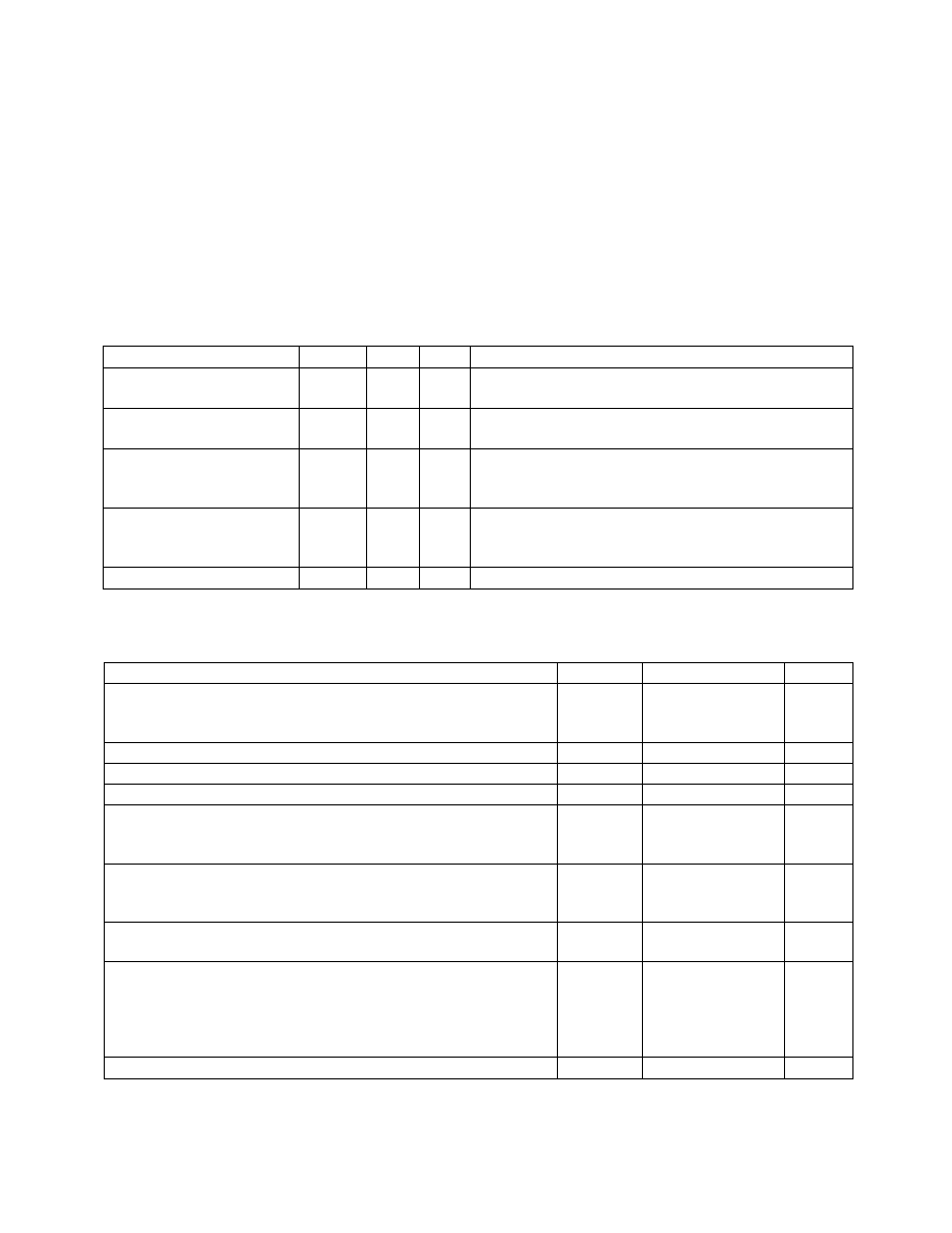
VDE 0884 (06.92) Insulation Characteristics
Description
Symbol
Characteristic
Unit
Installation classification per DIN VDE 0110, Table 1
for rated mains voltage
300 V
rms
I-IV
for rated mains voltage
600 V
rms
I-III
Climatic Classification
40/85/21
Pollution Degree (DIN VDE 0110, Table 1)*
2
Maximum Working Insulation Voltage
V
IORM
848
V
peak
Input to Output Test Voltage, Method b**
V
PR
= 1.875 x V
IORM
, Production test with t
p
= 1 sec,
V
PR
1591
V
peak
Partial discharge < 5 pC
Input to Output Test Voltage, Method a**
V
PR
= 1.5 x V
IORM
, Type and sample test, t
p
= 60 sec,
V
PR
1273
V
peak
Partial discharge < 5 pC
Highest Allowable Overvoltage**
V
TR
6000
V
peak
(Transient Overvoltage, t
TR
= 10 sec)
Safety-limiting values (Maximum values allowed in the event
of a failure, also see Figure 15)
Case Temperature
T
S
175
�
C
Input Power
P
S,INPUT
80
mW
Output Power
P
S,OUTPUT
250
mW
Insulation Resistance at T
S
, V
IO
= 500 V
R
S
1 x 10
12
*This part may also be used in Pollution Degree 3 environments where the rated mains voltage is
300 V
rms (per DIN VDE 0110).
**Refer to the front of the optocoupler section in the current catalog for a more detailed description of VDE 0884 and other product
safety requirements.
Insulation and Safety Related Specifications
Parameter
Symbol Value Units
Conditions
Min. External Air Gap
L(IO1)
7.4
mm
Measured from input terminals to output terminals,
(External Clearance)
shortest distance through air
Min. External Tracking
L(IO2)
8.0
mm
Measured from input terminals to output terminals,
Path (External Creepage)
shortest distance path along body
Min. Internal Plastic
0.5
mm
Through insulation distance, conductor to conductor,
Gap (Internal Clearance)
usually the direct distance between the photoemitter
and photodetector inside the optocoupler cavity
Tracking Resistance
CTI
175
V
DIN IEC 112/VDE 0303 PART 1
(Comparative
Tracking Index)
Isolation Group
IIIa
Material Group (DIN VDE 0110, 1/89, Table 1)
Option 300 � surface mount classification is Class A in accordance with CECC 00802.
Note: Optocouplers providing safe electrical separation per VDE 0884 do so only within the safety-limiting values to which they are
qualified. Protective cut-out switches must be used to ensure that the safety limits are not exceeded.
VDE
Approved according to VDE
0884/06.92
Regulatory Information
The HCPL-7100/1 has been
approved by the following
organizations:
UL
Recognized under UL 1577,
Component Recognition Program,
File E55361.
CSA
Approved under CSA Component
Acceptance Notice #5, File CA
88324.
1-406
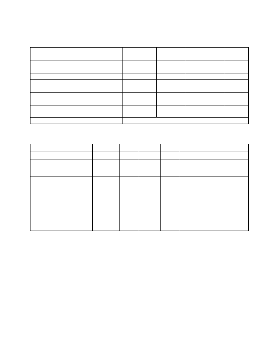
Parameter
Symbol
Min.
Max.
Unit
Storage Temperature
T
S
-55
125
�
C
Ambient Operating Temperature
T
A
-40
85
�
C
Supply Voltages
V
DD1,2
0.0
5.5
V
Input Voltage
V
I
-0.5
V
DD1
+ 0.5
V
Output Voltage
V
O
-0.5
V
DD2
+ 0.5
V
Output Enable Voltage
V
OE
-0.5
V
DD2
+ 0.5
V
Average Output Current
I
O
25
mA
Package Power Dissipation
P
PD
220
mW
Lead Solder Temperature
T
LS
260
�
C
(1.6 mm Below Seating Plane, 10 sec.)
Reflow Temperature Profile
See Package Outline Drawings Section
Parameter
Symbol
Min.
Max.
Unit
Test Conditions
Operating Temperature
T
A
-40
85
�
C
Supply Voltages
V
DD1,2
4.5
5.5
V
Logic High Input Voltage
V
IH
2.0
V
DD1
V
Logic Low Input Voltage
V
IL
0.0
0.8
V
Logic High Output
V
OEH
2.0
V
DD2
V
Output in high impedance
Enable Voltage
state
Logic Low Output
V
OEL
0.0
0.8
V
Output enabled
Enable Voltage
Input Signal Rise and
t
r
, t
f
1
ms
Fall Times
TTL Fanout
N
6
Standard Loads
Absolute Maximum Ratings
Recommended Operating Conditions