 | –≠–ª–µ–∫—Ç—Ä–æ–Ω–Ω—ã–π –∫–æ–º–ø–æ–Ω–µ–Ω—Ç: HCPL-7710 | –°–∫–∞—á–∞—Ç—å:  PDF PDF  ZIP ZIP |
Features
∑ +5 V CMOS compatibility
∑ 8 ns maximum pulse width
distortion
∑ 20 ns maximum prop. delay skew
∑ High speed: 12 Mbd
∑ 40 ns maximum prop. delay
∑ 10 kV/
µ
s minimum common mode
rejection
∑ -40
∞
C to 100
∞
C temperature range
∑ Safety and regulatory approvals
UL Recognized
3750 V rms for 1 min. per
UL 1577
CSA Component Acceptance
Notice #5
IEC/EN/DIN EN 60747-5-2
≠ V
IORM
= 630 Vpeak for
HCPL-7710 Option 060
≠ V
IORM
= 560 Vpeak for
HCPL-0710 Option 060
Applications
∑ Digital fieldbus isolation:
DeviceNet, SDS, Profibus
∑ AC plasma display panel level
shifting
∑ Multiplexed data transmission
∑ Computer peripheral interface
∑ Microprocessor system interface
Description
Available in either an 8-pin DIP or
SO-8 package style respectively,
the HCPL-7710 or HCPL-0710
optocouplers utilize the latest
CMOS IC technology to achieve
outstanding performance with
very low power consumption. The
HCPL-x710 require only two
bypass capacitors for complete
CMOS compatibility.
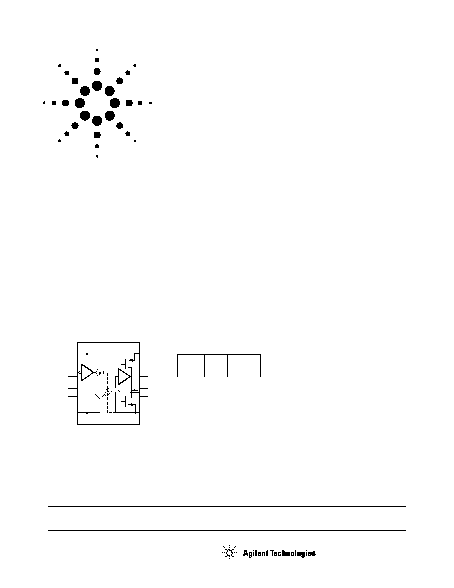
Functional Diagram
Basic building blocks of the
HCPL-x710 are a CMOS LED
driver IC, a high speed LED and a
CMOS detector IC. A CMOS logic
input signal controls the LED
driver IC which supplies current
to the LED. The detector IC
incorporates an integrated
photodiode, a high-speed
transimpedance amplifier, and a
voltage comparator with an
output driver.
CAUTION: It is advised that normal static precautions be taken in handling and assembly of this
component to prevent damage and/or degradation which may be induced by ESD.
* Pin 3 is the anode of the internal LED and must be left unconnected for guaranteed data sheet
performance. Pin 7 is not connected internally.
** A 0.1
µ
F bypass capacitor must be connected between pins 1 and 4, and 5 and 8.
8
7
6
1
3
SHIELD
5
2
4
**VDD1
VI
*
GND1
VDD2**
VO
GND2
VI, INPUT
LED1
H
L
OFF
ON
TRUTH TABLE
(POSITIVE LOGIC)
NC*
IO
LED1
VO, OUTPUT
H
L
Agilent HCPL-7710, HCPL-0710
40 ns Propagation Delay,
CMOS Optocoupler
Data Sheet
2
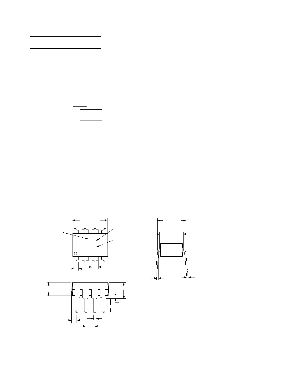
Package Outline Drawing
HCPL-7710 8-Pin DIP Package
9.65 ± 0.25
(0.380 ± 0.010)
1.78 (0.070) MAX.
1.19 (0.047) MAX.
A XXXXV
YYWW
DATE CODE
1.080 ± 0.320
(0.043 ± 0.013)
2.54 ± 0.25
(0.100 ± 0.010)
0.51 (0.020) MIN.
0.65 (0.025) MAX.
4.70 (0.185) MAX.
2.92 (0.115) MIN.
DIMENSIONS IN MILLIMETERS AND (INCHES).
5
6
7
8
4
3
2
1
5∞ TYP.
0.254
+ 0.076
- 0.051
(0.010
+ 0.003)
- 0.002)
7.62 ± 0.25
(0.300 ± 0.010)
6.35 ± 0.25
(0.250 ± 0.010)
TYPE NUMBER
*OPTION 300 AND 500 NOT MARKED.
NOTE: FLOATING LEAD PROTRUSION IS 0.25 mm (10 mils) MAX.
OPTION 060 CODE*
3.56 ± 0.13
(0.140 ± 0.005)
Selection Guide
8-Pin DIP
Small Outline
(300 Mil)
SO-8
HCPL-7710
HCPL-0710
Ordering Information
Specify Part Number followed by Option Number (if desired)
Example
HCPL-7710#XXXX
060 = IEC/EN/DIN EN 60747-5-2 Option.
300 = Gull Wing Surface Mount Option (HCPL-7710 only).
500 = Tape and Reel Packaging Option.
XXXE = Lead Free Option
No Option and Option 300 contain 50 units (HCPL-7710), 100 units (HCPL-0710) per tube.
Option 500 contain 1000 units (HCPL-7710), 1500 units (HCPL-0710) per reel.
Option data sheets available. Contact Agilent sales representative or authorized distributor.
Remarks: The notation "#" is used for existing products, while (new) products launched since 15th July 2001 and lead free option will use "≠"

3
Package Outline Drawing
HCPL-7710 Package with Gull Wing Surface Mount Option 300
Package Outline Drawing
HCPL-0710 Outline Drawing (Small Outline SO-8 Package)
0.635 ± 0.25
(0.025 ± 0.010)
12∞ NOM.
9.65 ± 0.25
(0.380 ± 0.010)
0.635 ± 0.130
(0.025 ± 0.005)
7.62 ± 0.25
(0.300 ± 0.010)
5
6
7
8
4
3
2
1
9.65 ± 0.25
(0.380 ± 0.010)
6.350 ± 0.25
(0.250 ± 0.010)
1.016 (0.040)
1.27 (0.050)
10.9 (0.430)
2.0 (0.080)
LAND PATTERN RECOMMENDATION
1.080 ± 0.320
(0.043 ± 0.013)
3.56 ± 0.13
(0.140 ± 0.005)
1.780
(0.070)
MAX.
1.19
(0.047)
MAX.
2.54
(0.100)
BSC
DIMENSIONS IN MILLIMETERS (INCHES).
LEAD COPLANARITY = 0.10 mm (0.004 INCHES).
NOTE: FLOATING LEAD PROTRUSION IS 0.25 mm (10 mils) MAX.
0.254
+ 0.076
- 0.051
(0.010
+ 0.003)
- 0.002)
XXXV
YWW
8
7
6
5
4
3
2
1
5.994 ± 0.203
(0.236 ± 0.008)
3.937 ± 0.127
(0.155 ± 0.005)
0.406 ± 0.076
(0.016 ± 0.003)
1.270
(0.050)
BSC
5.080 ± 0.127
(0.200 ± 0.005)
3.175 ± 0.127
(0.125 ± 0.005)
1.524
(0.060)
45∞ X
0.432
(0.017)
0.228 ± 0.025
(0.009 ± 0.001)
TYPE NUMBER
(LAST 3 DIGITS)
DATE CODE
0.305
(0.012)
MIN.
TOTAL PACKAGE LENGTH (INCLUSIVE OF MOLD FLASH)
5.207 ± 0.254 (0.205 ± 0.010)
DIMENSIONS IN MILLIMETERS (INCHES).
LEAD COPLANARITY = 0.10 mm (0.004 INCHES) MAX.
OPTION NUMBER 500 NOT MARKED.
NOTE: FLOATING LEAD PROTRUSION IS 0.15 mm (6 mils) MAX.
0.203 ± 0.102
(0.008 ± 0.004)
7∞
PIN ONE
0 ~ 7∞
*
*
7.49 (0.295)
1.9 (0.075)
0.64 (0.025)
LAND PATTERN RECOMMENDATION
4
All Agilent data sheets report the
creepage and clearance inherent
to the optocoupler component
itself. These dimensions are
needed as a starting point for the
equipment designer when
determining the circuit insulation
requirements. However, once
mounted on a printed circuit
board, minimum creepage and
clearance requirements must be
met as specified for individual
equipment standards. For
creepage, the shortest distance
path along the surface of a
printed circuit board between the
solder fillets of the input and
output leads must be considered.
There are recommended
techniques such as grooves and
ribs which may be used on a
printed circuit board to achieve
desired creepage and clearances.
Creepage and clearance distances
will also change depending on
factors such as pollution degree
and insulation level.
Regulatory Information
The HCPL-x710 have been
approved by the following
organizations:
UL
Recognized under UL 1577,
component recognition program,
File E55361.
CSA
Approved under CSA Component
Acceptance Notice #5, File CA
88324.
IEC/EN/DIN EN 60747-5-2
Approved under:
IEC 60747-5-2:1997 + A1:2002
EN 60747-5-2:2001 + A1:2002
DIN EN 60747-5-2 (VDE 0884
Teil 2):2003-01.
(Option 060 only)
Recommended Pb-Free IR Profile
0
TIME (SECONDS)
TEMPERATURE (
∞
C)
200
100
50
150
100
200
250
300
0
30
SEC.
50 SEC.
30
SEC.
160∞C
140∞C
150∞C
PEAK
TEMP.
245∞C
PEAK
TEMP.
240∞C
PEAK
TEMP.
230∞C
SOLDERING
TIME
200∞C
PREHEATING TIME
150∞C, 90 + 30 SEC.
2.5∞C ± 0.5∞C/SEC.
3∞C + 1∞C/≠0.5∞C
TIGHT
TYPICAL
LOOSE
ROOM
TEMPERATURE
PREHEATING RATE 3∞C + 1∞C/≠0.5∞C/SEC.
REFLOW HEATING RATE 2.5∞C ± 0.5∞C/SEC.
Solder Reflow Thermal Profile
Insulation and Safety Related Specifications
Value
Parameter
Symbol
7710
0710
Units
Conditions
Minimum External Air
L(I01)
7.1
4.9
mm
Measured from input terminals to output
Gap (Clearance)
terminals, shortest distance through air.
Minimum External
L(I02)
7.4
4.8
mm
Measured from input terminals to output
Tracking (Creepage)
terminals, shortest distance path along
body.
Minimum Internal Plastic
0.08
0.08
mm
Insulation thickness between emitter and
Gap (Internal Clearance)
detector; also known as distance through
insulation.
Tracking Resistance
CTI
175
175
Volts
DIN IEC 112/VDE 0303 Part 1
(Comparative Tracking
Index)
Isolation Group
IIIa
IIIa
Material Group (DIN VDE 0110, 1/89,
Table 1)
217 ∞C
RAMP-DOWN
6 ∞C/SEC. MAX.
RAMP-UP
3 ∞C/SEC. MAX.
150 - 200 ∞C
260 +0/-5 ∞C
t 25 ∞C to PEAK
60 to 150 SEC.
20-40 SEC.
TIME WITHIN 5 ∞C of ACTUAL
PEAK TEMPERATURE
t
p
t
s
PREHEAT
60 to 180 SEC.
t
L
T
L
T
smax
T
smin
25
T
p
TIME
TEMPERA
TURE
NOTES:
THE TIME FROM 25 ∞C to PEAK TEMPERATURE = 8 MINUTES MAX.
T
smax
= 200 ∞C, T
smin
= 150 ∞C
5
IEC/EN/DIN EN 60747-5-2 Insulation Related Characteristics (Option 060)
HCPL-7710
HCPL-0710
Description
Symbol
Option 060
Option 060
Units
Installation classification per DIN VDE 0110/1.89, Table 1
for rated mains voltage
150 V rms
I-IV
I-IV
for rated mains voltage
300 V rms
I-IV
I-III
for rated mains voltage
450 V rms
I-III
Climatic Classification
55/100/21
55/100/21
Pollution Degree (DIN VDE 0110/1.89)
2
2
Maximum Working Insulation Voltage
V
IORM
630
560
V peak
Input to Output Test Voltage, Method b
V
PR
1181
1050
V peak
V
IORM
x 1.875 = V
PR
, 100% Production
Test with t
m
= 1 sec, Partial Discharge < 5 pC
Input to Output Test Voltage, Method a
V
PR
945
840
V peak
V
IORM
x 1.5 = V
PR
, Type and Sample Test,
t
m
= 60 sec, Partial Discharge < 5 pC
Highest Allowable Overvoltage
V
IOTM
6000
4000
V peak
(Transient Overvoltage, t
ini
= 10 sec)
Safety Limiting Values
(Maximum values allowed in the event of a failure,
also see Thermal Derating curve, Figure 11.)
Case Temperature
T
S
175
150
∞
C
Input Current
I
S,INPUT
230
150
mA
Output Power
P
S,OUTPUT
600
600
mW
Insulation Resistance at T
S
, V
10
= 500 V
R
IO
10
9
10
9
Refer to the front of the optocoupler section of the Isolation and Control Component Designer's Catalog, under Product Safety Regulations section
IEC/EN/DIN EN 60747-5-2, for a detailed description.
Note: These optocouplers are suitable for "safe electrical isolation" only within the safety limit data. Maintenance of the safety data shall be ensured
by means of protective circuits.
Note: The surface mount classification is Class A in accordance with CECC 00802.
Absolute Maximum Ratings
Parameter
Symbol
Min.
Max.
Units
Figure
Storage Temperature
T
S
≠55
125
∞
C
Ambient Operating Temperature
T
A
≠40
+100
∞
C
Supply Voltages
V
DD1
, V
DD2
0
6.0
Volts
Input Voltage
V
I
≠0.5
V
DD1
+0.5
Volts
Output Voltage
V
O
≠0.5
V
DD2
+0.5
Volts
Input Current
I
I
≠10
+10
mA
Average Output Current
I
O
10
mA
Lead Solder Temperature
260
∞
C for 10 sec., 1.6 mm below seating plane
Solder Reflow Temperature Profile
See Solder Reflow Temperature Profile Section
Recommended Operating Conditions
Parameter
Symbol
Min.
Max.
Units
Figure
Ambient Operating Temperature
T
A
≠40
+100
∞
C
Supply Voltages
V
DD1
, V
DD2
4.5
5.5
V
Logic High Input Voltage
V
IH
2.0
V
DD1
V
1, 2
Logic Low Input Voltage
V
IL
0.0
0.8
V
Input Signal Rise and Fall Times
t
r
, t
f
1.0
ms