 | –≠–ª–µ–∫—Ç—Ä–æ–Ω–Ω—ã–π –∫–æ–º–ø–æ–Ω–µ–Ω—Ç: HCPL-7800 | –°–∫–∞—á–∞—Ç—å:  PDF PDF  ZIP ZIP |
1-216
H
High CMR Isolation Amplifiers
Technical Data
HCPL-7800
HCPL-7800A
HCPL-7800B
applications, we recommend the
HCPL-7800 which exhibits a
part-to-part gain tolerance of
±
5%. For precision applications,
HP offers the HCPL-7800A and
HCPL-7800B, each with part-to-
part gain tolerances of
±
1%.
The HCPL-7800 utilizes sigma-
delta (
) analog-to-digital
converter technology, chopper
stabilized amplifiers, and a fully
differential circuit topology
fabricated using HP's 1
µ
m
CMOS IC process. The part also
couples our high-efficiency, high-
speed AlGaAs LED to a high-
speed, noise-shielded detector
∑ Switch-Mode Power Supply
Signal Isolation
∑ General Purpose Analog
Signal Isolation
∑ Transducer Isolation
Description
The HCPL-7800 high CMR
isolation amplifier provides a
unique combination of features
ideally suited for motor control
circuit designers. The product
provides the precision and
stability needed to accurately
monitor motor current in high-
noise motor control environ-
ments, providing for smoother
control (less "torque ripple") in
various types of motor control
applications.
This product paves the way for a
smaller, lighter, easier to produce,
high noise rejection, low cost
solution to motor current
sensing. The product can also be
used for general analog signal
isolation applications requiring
high accuracy, stability and
linearity under similarly severe
noise conditions. For general
CAUTION: It is advised that normal static precautions be taken in handling and assembly of this component to
prevent damage and/or degradation which may be induced by ESD.
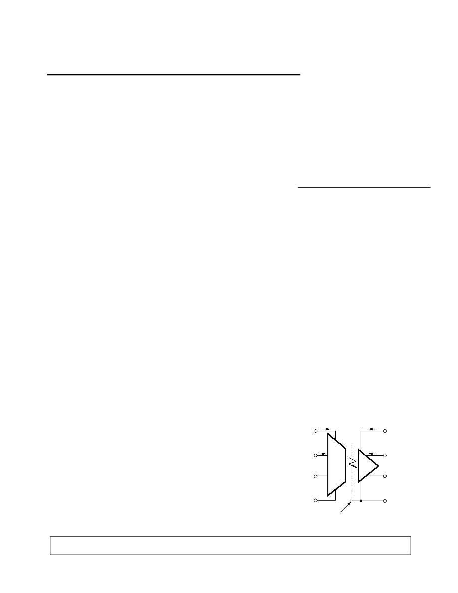
Functional Diagram
Features
∑ 15 kV/
µ
s Common-Mode
Rejection at V
CM
= 1000 V*
∑ Compact, Auto-Insertable
Standard 8-pin DIP Package
∑ 4.6
µ
V/
∞
C Offset Drift vs.
Temperature
∑ 0.9 mV Input Offset Voltage
∑ 85 kHz Bandwidth
∑ 0.1% Nonlinearity
∑ Worldwide Safety Approval:
UL 1577 (3750 V rms/1 min),
VDE 0884 and CSA
∑ Advanced Sigma-Delta (
)
A/D Converter Technology
∑ Fully Differential Circuit
Topology
∑ 1
µ
m CMOS IC Technology
Applications
∑ Motor Phase Current
Sensing
∑ General Purpose Current
Sensing
∑ High-Voltage Power Source
Voltage Monitoring
*The terms common-mode rejection
(CMR) and isolation-mode rejection (IMR)
are used interchangeably throughout this
data sheet.
1
2
3
4
8
7
6
5
V
DD1
V
IN+
V
IN-
GND1
V
DD2
V
OUT+
V
OUT-
GND2
CMR SHIELD
I
DD1
I
DD2
I
IN
I
O
+
+
-
-
5965-3592E

1-217
Ordering Information:
HCPL-7800x
No Specifier =
±
5% Gain Tol.; Mean Gain Value = 8.00
A =
±
1% Gain Tol.; Mean Gain Value = 7.93
B =
±
1% Gain Tol.; Mean Gain Value = 8.07
Option yyy
300 = Gull Wing Surface Mount Lead Option
500 = Tape/Reel Package Option (1 k min.)
Option datasheets available. Contact your Hewlett-Packard sales representative or authorized distributor for
information.
using our patented "light-pipe"
optocoupler packaging
technology.
Together, these features deliver
unequaled isolation-mode noise
rejection, as well as excellent
offset and gain accuracy and
stability over time and tempera-
ture. This performance is
delivered in a compact, auto-
insertable, industry standard 8-
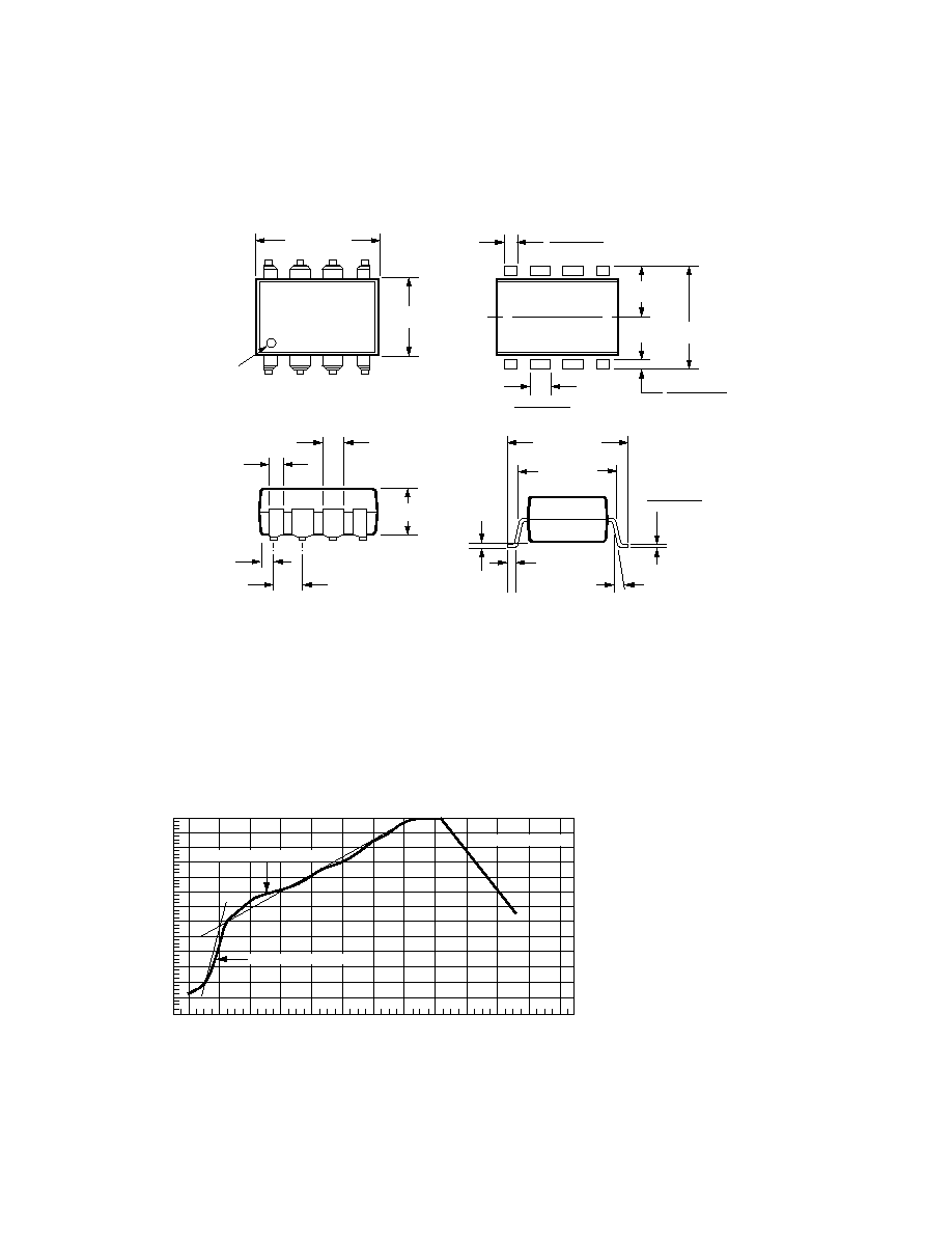
Package Outline Drawings
Standard DIP Package
pin DIP package that meets
worldwide regulatory safety
standards (gull-wing surface
mount option #300 also
available).
9.40 (0.370)
9.90 (0.390)
PIN ONE
1.78 (0.070) MAX.
1.19 (0.047) MAX.
HP 7800
YYWW
DATE CODE
0.76 (0.030)
1.24 (0.049)
2.28 (0.090)
2.80 (0.110)
0.51 (0.020) MIN.
0.65 (0.025) MAX.
4.70 (0.185) MAX.
2.92 (0.115) MIN.
6.10 (0.240)
6.60 (0.260)
0.20 (0.008)
0.33 (0.013)
5∞ TYP.
7.36 (0.290)
7.88 (0.310)
* TYPE NUMBER FOR: HCPL-7800 = 7800
1
2
3
4
8
7
6
5
5
6
7
8
4
3
2
1
GND1
VDD1
VIN+
VIN≠
GND2
VDD2
VOUT+
VOUT≠
PIN DIAGRAM
PIN ONE
TYPE NUMBER*
HCPL-7800A = 7800A
HCPL-7800B = 7800B
DIMENSIONS IN MILLIMETERS AND (INCHES).
1-218
Maximum Solder Reflow Thermal Profile
240
T = 115∞C, 0.3∞C/SEC
0
T = 100∞C, 1.5∞C/SEC
T = 145∞C, 1∞C/SEC
TIME ≠ MINUTES
TEMPERATURE ≠ ∞C
220
200
180
160
140
120
100
80
60
40
20
0
260
1
2
3
4
5
6
7
8
9
10
11
12
(NOTE: USE OF NON-CHLORINE ACTIVATED FLUXES IS RECOMMENDED.)
Gull Wing Surface Mount Option 300*
0.635 ± 0.25
(0.025 ± 0.010)
12∞ NOM.
0.20 (0.008)
0.33 (0.013)
9.65 ± 0.25
(0.380 ± 0.010)
0.51 ± 0.130
(0.020 ± 0.005)
7.62 ± 0.25
(0.300 ± 0.010)
5
6
7
8
4
3
2
1
9.65 ± 0.25
(0.380 ± 0.010)
6.350 ± 0.25
(0.250 ± 0.010)
1.02 (0.040)
1.19 (0.047)
1.19 (0.047)
1.78 (0.070)
9.65 ± 0.25
(0.380 ± 0.010)
4.83
(0.190)
TYP.
0.380 (0.015)
0.635 (0.025)
PIN LOCATION (FOR REFERENCE ONLY)
1.080 ± 0.320
(0.043 ± 0.013)
4.19
(0.165)
MAX.
1.780
(0.070)
MAX.
1.19
(0.047)
MAX.
2.540
(0.100)
BSC
DIMENSIONS IN MILLIMETERS (INCHES).
TOLERANCES (UNLESS OTHERWISE SPECIFIED):
* REFER TO OPTION 300 DATA SHEET FOR MORE INFORMATION.
xx.xx = 0.01
xx.xxx = 0.005
HP 7800
YYWW
MOLDED
LEAD COPLANARITY
MAXIMUM: 0.102 (0.004)
1-219
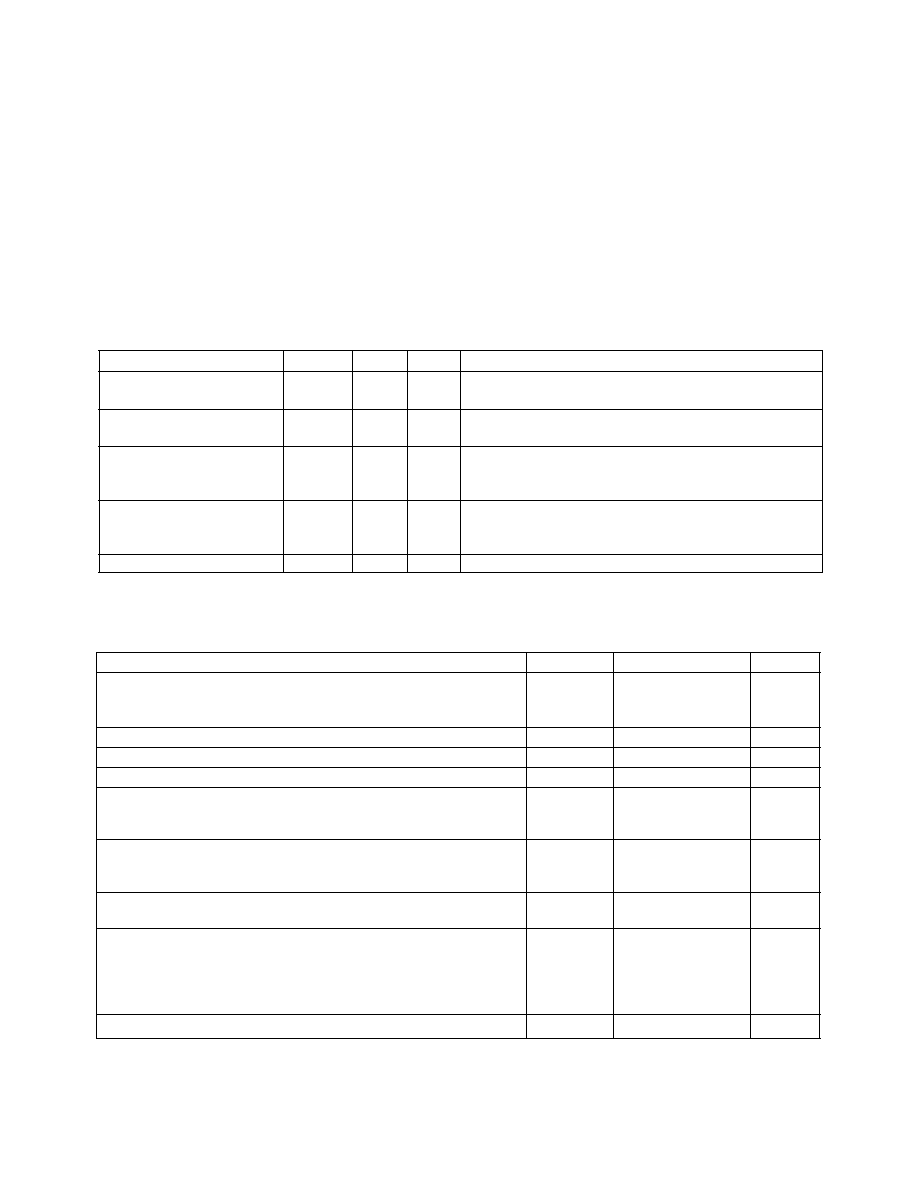
VDE 0884 (06.92) Insulation Characteristics
Description
Symbol
Characteristic
Unit
Installation classification per DIN VDE 0110, Table 1
for rated mains voltage
300 V rms
I-IV
for rated mains voltage
600 V rms
I-III
Climatic Classification
40/100/21
Pollution Degree (DIN VDE 0110, Table 1)*
2
Maximum Working Insulation Voltage
V
IORM
848
V
peak
Input to Output Test Voltage, Method b**
V
PR
1591
V
peak
V
PR
= 1.875 x V
IORM
, Production test with t
p
= 1 sec,
Partial discharge < 5 pC
Input to Output Test Voltage, Method a**
V
PR
1273
V
peak
V
PR
= 1.5 x V
IORM
, Type and sample test with t
p
= 60 sec,
Partial discharge < 5 pC
Highest Allowable Overvoltage**
(Transient Overvoltage t
TR
= 10 sec)
V
TR
6000
V
peak
Safety-limiting values (Maximum values allowed in the event
of a failure, also see Figure 27)
Case Temperature
T
S
175
∞
C
Input Power
P
S,Input
80
mW
Output Power
P
S,Output
250
mW
Insulation Resistance at T
S
, V
IO
= 500 V
R
S
1x10
12
*This part may also be used in Pollution Degree 3 environments where the rated mains voltage is
300 V rms (per DIN VDE 0110).
**Refer to the front of the optocoupler section of the current catalog for a more detailed description of VDE 0884 and other product
safety requirements.
Note: Optocouplers providing safe electrical separation per VDE 0884 do so only within the safety-limiting values to which they are
qualified. Protective cut-out switches must be used to ensure that the safety limits are not exceeded.
Regulatory Information
The HCPL-7800 has been
approved by the following
organizations:
UL
Recognized under UL 1577,
Component Recognition
Program, File E55361.
CSA
Approved under CSA Component
Acceptance Notice #5, File CA
88324.
Insulation and Safety Related Specifications
Parameter
Symbol
Value Units
Conditions
Min. External Air Gap
L(IO1)
7.4
mm
Measured from input terminals to output terminals,
(External Clearance)
shortest distance through air
Min. External Tracking
L(IO2)
8.0
mm
Measured from input terminals to output terminals,
Path (External Creepage)
shortest distance path along body
Min. Internal Plastic Gap
0.5
mm
Through insulation distance, conductor to conductor,
(Internal Clearance)
usually the direct distance between the photoemitter
and photodetector inside the optocoupler cavity
Tracking Resistance
CTI
175
V
DIN IEC 112/VDE 0303 Part 1
(Comparative Tracking
Index)
Isolation Group
III a
Material Group (DIN VDE 0110, 1/89, Table 1)
Option 300 ≠ surface mount classification is Class A in accordance with CECC 00802.
VDE
Approved according to VDE
0884/06.92.
1-220
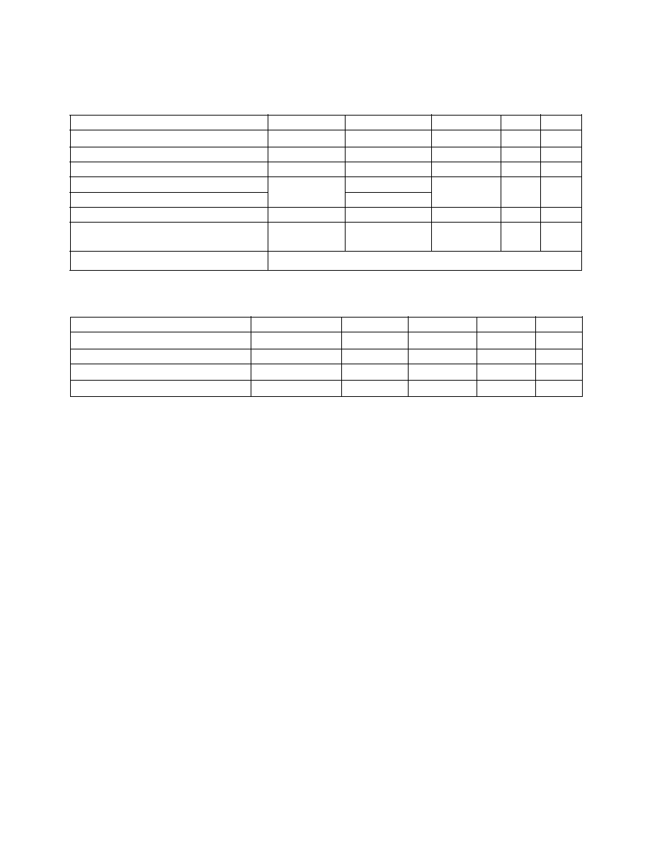
Absolute Maximum Ratings
Parameter
Symbol
Min.
Max.
Unit
Note
Storage Temperature
T
S
-55
125
∞
C
Ambient Operating Temperature
T
A
-
40
100
∞
C
Supply Voltages
V
DD1
, V
DD2
0.0
5.5
V
Steady-State Input Voltage
V
IN+
, V
IN-
-2.0
V
DD1
+0.5
V
Two Second Transient Input Voltage
-6.0
Output Voltages
V
OUT+
, V
OUT-
-0.5
V
DD2
+0.5
V
Lead Solder Temperature
T
LS
260
∞
C
1
(1.6 mm below seating plane, 10 sec.)
Reflow Temperature Profile
See Package Outline Drawings Section
Recommended Operating Conditions
Parameter
Symbol
Min.
Max.
Unit
Note
Ambient Operating Temperature
T
A
-40
85
∞
C
2
Supply Voltages
V
DD1
, V
DD2
4.5
5.5
V
3
Input Voltage
V
IN+
, V
IN-
-200
200
mV
4
Output Current
|I
O
|
1
mA
5