 | –≠–ª–µ–∫—Ç—Ä–æ–Ω–Ω—ã–π –∫–æ–º–ø–æ–Ω–µ–Ω—Ç: HCPL-7860 | –°–∫–∞—á–∞—Ç—å:  PDF PDF  ZIP ZIP |
1-260
H
CAUTION: It is advised that normal static precautions be taken in handling and assembly of this component to
prevent damage and/or degradation which may be induced by ESD.
Isolated 15-bit A/D Converter
Technical Data
HCPL-7860
HCPL-0870, -7870
Features
∑ 12-bit Linearity
∑ 700 ns Conversion Time
(Pre-Trigger Mode 2)
∑ 5 Conversion Modes for
Resolution/Speed Trade-Off;
12-bit Effective Resolution
with 18
µ
s Signal Delay
(14-bit with 94
µ
s)
∑ Fast 3
µ
s Over-Range
Detection
∑ Serial I/O (SPI
Æ
, QSPI
Æ
and
Microwire
Æ
Compatible)
∑
±
200 mV Input Range with
Single 5 V Supply
∑ 1% Internal Reference
Voltage Matching
Hewlett-Packard's Isolated A/D Converter delivers the reliability, small size, superior
isolation and over-temperature performance motor drive designers need to accurately
measure current at half the price of traditional solutions.
SPI and QSPI are trademarks of Motorola Corp.
Microwire is a trademark of National Semiconductor Inc.
∑ Offset Calibration
∑ -40
∞
C to +85
∞
C Operating
Temperature Range
∑ 15 kV/
µ
s Isolation Transient
Immunity
∑ Regulatory Approvals; UL,
CSA, VDE
HP7860
YYWW
HPx870
YYWW
DIGITAL
INTERFACE IC
ISOLATED
MODULATOR
ISOLATION
BOUNDARY
+
+
INPUT
CURRENT
OUTPUT
DATA
MICRO-CONTROLLER
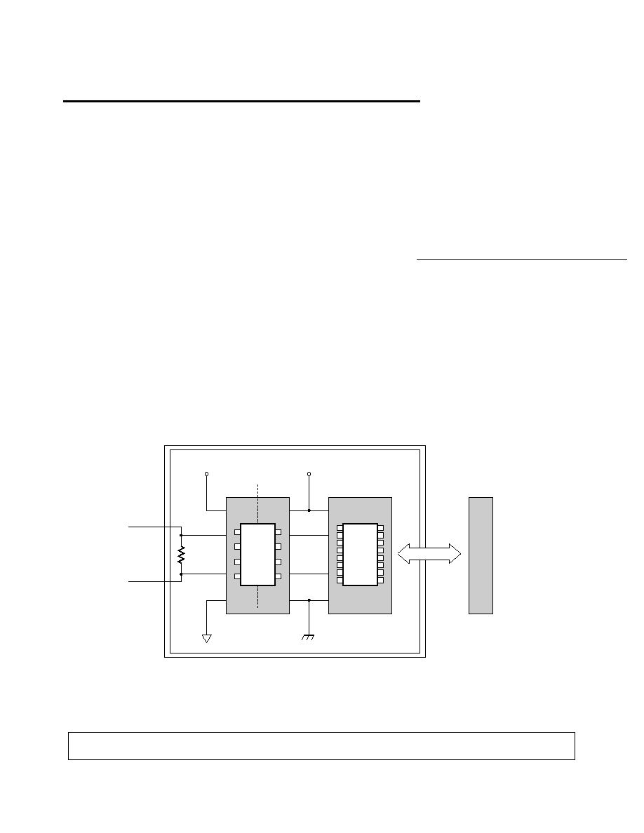
DIGITAL CURRENT SENSOR
5965-5255E
1-261
RSHUNT
0.02
INPUT
CURRENT
VDD1
ISOLATED
+ 5 V
VIN+
VIN-
GND1
VDD2
MCLK
MDAT
GND2
C1
0.1 µF
+
CDAT
SCLK
CCLK
VDD
CLAT
CHAN
MCLK1
SDAT
MDAT1
CS
MCLK2
THR1
MDAT2
OVR1
GND
RESET
NON-ISOLATED
+ 5 V
C3
10 µF
+
HCPL-7860
3-WIRE
SERIAL
INTERFACE
C2
0.1 µF
HCPL-x870
Digital Current Sensing
Circuit
As shown in Figure 1, using the
Isolated 2-chip A/D converter to
sense current can be as simple as
connecting a current-sensing
resistor, or shunt, to the input
and reading output data through
the 3-wire serial output interface.
By choosing the appropriate
shunt resistance, any range of
current can be monitored, from
less than 1 A to more than 100 A.
Even better performance can be
achieved by fully utilizing the
more advanced features of the
Isolated A/D converter, such as
the pre-trigger circuit which can
reduce conversion time to less
Figure 1: Typical Application Circuit.
Product Overview
Description
The HCPL-7860 Isolated Modu-
lator and the HCPL-x870 Digital
Interface IC together form an
isolated programmable two-chip
analog-to-digital converter. The
isolated modulator allows direct
measurement of motor phase
currents in power inverters while
the digital interface IC can be
programmed to optimize the
conversion speed and resolution
trade-off.
In operation, the HCPL-7860
Isolated Modulator (optocoupler
with 3750 V
RMS
dielectric with-
stand voltage rating) converts a
low-bandwidth analog input into
a high-speed one-bit data stream
by means of a sigma-delta (
)
oversampling modulator. This
modulation provides for high
noise margins and excellent
immunity against isolation-mode
transients. The modulator data
and on-chip sampling clock are
encoded and transmitted across
the isolation boundary where they
are recovered and decoded into
separate high-speed clock and
data channels.
The Digital Interface IC converts
the single-bit data stream from
the Isolated Modulator into
fifteen-bit output words and
provides a serial output interface
that is compatible with SPI
Æ
,
QSPI
Æ
, and Microwire
Æ
proto-
cols, allowing direct connection
to a microcontroller. The Digital
Interface IC is available in two
package styles: the HCPL-7870 is
in a 16-pin DIP package and the
HCPL-0870 is in a 300-mil wide
SO-16 surface-mount package.
Features of the Digital Interface
IC include five different conver-
sion modes, three different pre-
trigger modes, offset calibration,
fast over-range detection, and
adjustable threshold detection.
Programmable features are con-
figured via the Serial Configura-
tion port. A second multiplexed
input is available to allow
measurements with a second
than 1
µ
s, the fast over-range
detector for quickly detecting
short circuits, different conversion
modes giving various resolution/
speed trade-offs, offset calibra-
tion mode to eliminate initial
offset from measurements, and
an adjustable threshold detector
for detecting non-short circuit
overload conditions.

1-262
isolated modulator without
additional hardware. Because the
two inputs are multiplexed, only
one conversion at a time can be
made and not all features are
available for the second channel.
The available features for both
channels are shown in the table
at right.
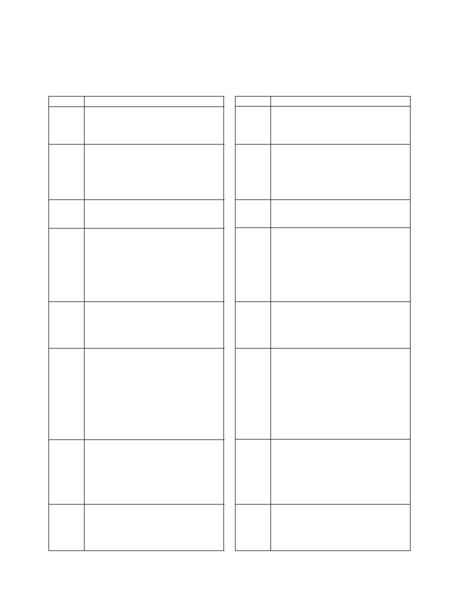
HCPL-x870 Digital Interface IC
Feature
Channel #1
Channel #2
Conversion Mode
Offset Calibration
Pre-Trigger Mode
Over-Range Detection
Adjustable Threshold Detection
5
6
12
11
MDAT1
MCLK2
CS
THR1
CON-
VERSION
INTER-
FACE
CONFIG.
INTER-
FACE
7
10
MDAT2
OVR1
8
9
GND
RESET
1
2
16
15
CCLK
CLAT
VDD
CHAN
3
14
CDAT
SCLK
4
13
MCLK1
SDAT
CH1
CH2
THRES-
HOLD
DETECT
&
RESET
Functional Diagrams
Pin Description, Isolated Modulator
Symbol
Description
Symbol
Description
V
DD1
Supply voltage input (4.5 V to 5.5 V)
V
DD2
Supply voltage input (4.5 V to 5.5 V)
V
IN+
Positive input (
±
200 mV
MCLK
Clock output (10 MHz typical)
recommended)
V
IN≠
Negative input
MDAT
Serial data output
(normally connected to GND1)
GND1
Input ground
GND2
Output ground
HCPL-7860 Isolated Modulator
HCPL-x870 Digital Interface IC
1
2
3
4
8
7
6
5
VDD1
VIN+
VIN≠
GND1
VDD2
MCLK
MDAT
GND2
SHIELD
ISOLATION
BOUNDARY
DECODE
SIGMA-
DELTA
MOD./
ENCODE
1-263
Pin Description, Digital Interface IC
Symbol
Description
CCLK
Clock input for the Serial Configuration
Interface (SCI). Serial Configuration
data is clocked in on the rising edge
of CCLK.
CLAT
Latch input for the Serial Configuration
Interface (SCI). The last 8 data bits
clocked in on CDAT by CCLK are
latched into the appropriate
configuration register on the rising
edge of CLAT.
CDAT
Data input for the Serial Configuration
Interface (SCI). Serial configuration
data is clocked in MSB first.
MCLK1
Channel 1 Isolated Modulator clock
input. Input Data on MDAT1 is clocked
in on the rising edge of MCLK1.
MDAT1
Channel 1 Isolated Modulator data
input.
MCLK2
Channel 2 Isolated Modulator clock
input. Input Data on MDAT2 is clocked
in on the rising edge of MCLK2.
MDAT2
Channel 2 Isolated Modulator data
input.
GND
Digital ground.
Symbol
Description
V
DD
Supply voltage (4.5 V to 5.5 V).
CHAN
Channel select input. The input level on
CHAN determines which channel of
data is used during the next conversion
cycle. An input low selects channel 1,
a high selects channel 2.
SCLK
Serial clock input. Serial data is clocked
out of SDAT on the falling edge of SCLK.
SDAT
Serial data output. SDAT changes from
high impedance to a logic low output
at the start of a conversion cycle.
SDAT then goes high to indicate that
data is ready to be clocked out. SDAT
returns to a high-impedance state after
all data has been clocked out and CS
has been brought high.
CS
Conversion start input. Conversion
begins on the falling edge of CS. CS
should remain low during the entire
conversion cycle and then be brought
high to conclude the cycle.
THR1
Continuous, programmable-threshold
detection for channel 1 input data. A
high level output on THR1 indicates
that the magnitude of the channel 1
input signal is beyond a user
programmable threshold level between
160 mV and 310 mV. This signal
continuously monitors channel 1
independent of the channel select
(CHAN) signal.
OVR1
High speed continuous over-range
detection for channel 1 input data. A
high level output on OVR1 indicates
that the magnitude of the channel 1
input is beyond full-scale. This signal
continuously monitors channel 1
independent of the CHAN signal.
RESET
Master reset input. A logic high input
for at least 100 ns asynchronously
resets all configuration registers to
their default values and zeroes the
Offset Calibration registers.
1-264
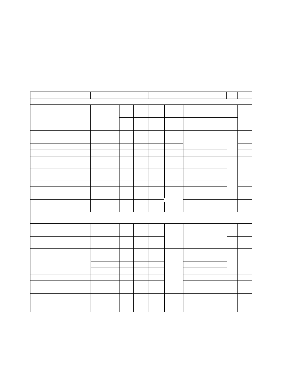
Isolated A/D Converter Performance
Electrical Specifications
Unless otherwise noted, all specifications are at V
IN+
= -200 mV to +200 mV and V
IN-
= 0 V; all Typical
specifications are at T
A
= 25
∞
C and V
DD1
= V
DD2
= V
DD
= 5 V; all Minimum/Maximum specifications are at
T
A
= -40
∞
C to +85
∞
C, V
DD1
= V
DD2
= V
DD
= 4.5 to 5.5 V.
Parameter
Symbol
Min.
Typ.
Max.
Units
Test Conditions
Fig. Note
STATIC CONVERTER CHARACTERISTICS
Resolution
15
bits
1
Integral Nonlinearity
INL
6
30
LSB
3
2
0.025
0.14
%
4
Differential Nonlinearity
DNL
1
LSB
3
Uncalibrated Input Offset
V
OS
-1
1
2.5
mV
V
IN+
= 0 V
5
Offset Drift vs. Temperature
dV
OS
/dT
A
4
µ
V/
∞
C
4
Offset drift vs. V
DD1
dV
OS
/dV
DD1
0.7
mV/V
Internal Reference Voltage
V
REF
326
mV
Absolute Reference Voltage
-4
4
%
6
5
Tolerance
Reference Voltage
-1
1
%
T
A
= 25
∞
C.
Matching
See Note 5
V
REF
Drift vs. Temperature
dV
REF
/dT
A
190
ppm/
∞
C
V
REF
Drift vs. V
DD1
dV
REF
/dV
DD1
0.9
%
Full Scale Input Range
-V
REF
+V
REF
mV
6
Recommended Input
-200
+200
Voltage Range
DYNAMIC CONVERTER CHARACTERISTICS
(Digital Interface IC is set to Conversion Mode 3.)
Signal-to-Noise Ratio
SNR
62
73
dB
V
IN+
= 35 Hz,
2,9
Total Harmonic Distortion
THD
-67
Signal-to-(Noise
SND
66
+ Distortion)
Effective Number of Bits
ENOB
10
12
bits
8
7
Conversion Time
t
C2
0.7
1.0
µ
s
Pre-Trigger Mode 2
7,
8
t
C1
18
22
Pre-Trigger Mode 1
t
C0
37
44
Pre-Trigger Mode 0
Signal Delay
t
DSIG
18
22
10
9
Over-Range Detect Time
t
OVR1
2.0
2.7
4.2
V
IN+
= 0 to 400 mV 12
10
Threshold Detect Time
t
THR1
10
11
Signal Bandwidth
BW
18
22
kHz
11
12
Isolation Transient
CMR
15
20
kV/
µ
s
V
ISO
= 1 kV
13
Immunity
400 mV
pk-pk
(141 mV
rms
) sine
wave.
step waveform
14