 | –≠–ª–µ–∫—Ç—Ä–æ–Ω–Ω—ã–π –∫–æ–º–ø–æ–Ω–µ–Ω—Ç: HCPL-M456 | –°–∫–∞—á–∞—Ç—å:  PDF PDF  ZIP ZIP |
Document Outline
- Selector Guide
- List of Figures
- 1. HCPL-4506 Outline Drawing (Standard DIP Package).
- 2. HCPL-4506 Gull Wing Surface Mount Option #300 Outline Drawing.
- 3. HCPL-0466 Outline Drawing (8-Pin Small Outline Package).
- 4a. HCNW4506 Outline Drawing (8-Pin Widebody Package).
- 4b. HCNW4506 Outline Drawing (8-Pin Widebody Package with Gull Wing Surface Mount Option 300).
- 5. Typical Transfer Characteristics
- 6. Normalized Output Current vs. Temperature.
- 7. High Level Output Current vs. Temperature.
- 8. HCPL-4506 and HCPL-0466 Input Current vs. Forward Voltage.
- 9. HCNW4506 Input Current vs. Forward Voltage.
- 10. Propagation Delay Test Circuit.
- 11. CMR Test Circuit. Typical CMR Waveform.
- 12. Propagation Delay with External 20 kW RL vs. Temperature.
- 13. Propagation Delay with Internal 20 kW RL vs. Temperature.
- 14. Propagation Delay vs. Load Resistance.
- 15. Propagation Delay vs. Load Capacitance.
- 16. Propagation Delay vs. Supply Voltage.
- 17. Propagation Delay vs. Input Current.
- 18. Thermal Derating Curve, Dependence of Safety Limiting Value with Case Temperature per VDE 0884.
- 19. Recommended LED Drive Circuit.
- 20. Optocoupler Input to Output Capacitance Model for Unshielded Optocouplers.
- 21. Optocoupler Input to Output Capacitance Model for Shielded Optocouplers.
- 22. LED Drive Circuit with Resistor Connected to LED Anode (Not Recommended).
- 23. AC Equivalent Circuit for Figure 22 During Common Mode Transients.
- 24. AC Equivalent Circuit for Figure 19 During Common Mode Transients.
- 25. Not Recommended Open Collector LED Drive Circuit.
- 26. AC Equivalent Circuit for Figure 25 During Common Mode Transients.
- 27. Recommended LED Drive Circuit for Ultra High CMR.
- 28. Typical Application Circuit.
- 29. Minimum LED Skew for Zero Dead Time.
- 30. Waveforms for Dead Time Calculation.
- Features
- Applications
- Description
- Functional Diagram
- Truth Table
- Selection Guide
- Ordering Information
- Package Outline Drawings
- Pin Location (for reference only)
- Solder Reflow Temperature Profile
- Regulatory Information
- Insulation and Safety Related Specifications
- VDE 0884 Insulation Related Characteristics (HCPL-4506 OPTION 060 ONLY)
- VDE 0884 Insulation Related Characteristics (HCNW4506 ONLY)
- Absolute Maximum Ratings
- Recommended Operating Conditions
- Electrical Specifications
- Switching Specifications (R L = 20 kO External)
- Switching Specifications (R L = Internal Pull-up)
- Package Characteristics
- LED Drive Circuit Considerations for Ultra High CMR Performance
- CMR with the LED On (CMR L )
- CMR with the LED Off (CMR H )
- IPM Dead Time and Propagation Delay Specifications

1-49
H
Intelligent Power Module and
Gate Drive Interface Optocouplers
Technical Data
Features
∑ Performance Specified for
Common IPM Applications
over Industrial Temperature
Range: -40
∞
C to 100
∞
C
∑ Fast Maximum Propagation
Delays
t
PHL
= 400 ns
t
PLH
= 550 ns
∑ Minimized Pulse Width
Distortion (PWD = 450 ns)
∑ 15 kV/
µ
s Minimum Common
Mode Transient Immunity at
V
CM
= 1500 V
∑ CTR > 44% at I
F
= 10 mA
∑ Safety Approval
UL Recognized - 2500 V rms
for 1 minute (5000 V rms for
1 minute for HCNW4506 and
HCPL-4506 Option 020) per
UL1577
CSA Approved
VDE 0884 Approved
-V
IORM
= 630 V
peak
for
HCPL-4506 Option 060
-V
IORM
= 1414 V
peak
for
HCNW4506
BSI Certified (HCNW4506)
Applications
∑ IPM Isolation
∑ Isolated IGBT/MOSFET Gate
Drive
∑ AC and Brushless DC Motor
Drives
∑ Industrial Inverters
Description
The HCPL-4506 and HCPL-0466
contain a GaAsP LED while the
HCNW4506 contains an AlGaAs
LED. The LED is optically
coupled to an integrated high gain
photo detector. Minimized propa-
The connection of a 0.1
µ
F bypass capacitor between pins 5 and 8 is recommended.
gation delay difference between
devices make these optocouplers
excellent solutions for improving
inverter efficiency through
reduced switching dead time.
An on chip 20 k
output pull-up
resistor can be enabled by short-
ing output pins 6 and 7, thus
eliminating the need for an
external pull-up resistor in
common IPM applications. Speci-
fications and performance plots
are given for typical IPM
applications.
HCPL-4506
HCPL-0466
HCNW4506
Functional Diagram
Truth Table
LED
V
O
ON
L
OFF
H
8
7
6
1
3
SHIELD
5
2
4
20 k
NC
ANODE
CATHODE
NC
VCC
VL
VO
GND
CAUTION: It is advised that normal static precautions be taken in handling and assembly of this component to
prevent damage and/or degradation which may be induced by ESD.
Selection Guide
Operating Temperature
T
A
[
∞
C]
Single Channel Packages
8-Pin DIP
Small Outline
Widebody
Min.
Max.
(300 Mil)
SO-8
(400 Mil)
Hermetic*
-40
100
HCPL-4506
HCPL-0466
HCNW4506
-55
125
HCPL-5300
HCPL-5301
*Technical data for these products are on separate HP publications.
5965-3603E

1-50
0.635 ± 0.25
(0.025 ± 0.010)
12∞ NOM.
9.65 ± 0.25
(0.380 ± 0.010)
0.635 ± 0.130
(0.025 ± 0.005)
7.62 ± 0.25
(0.300 ± 0.010)
5
6
7
8
4
3
2
1
9.65 ± 0.25
(0.380 ± 0.010)
6.350 ± 0.25
(0.250 ± 0.010)
1.016 (0.040)
1.194 (0.047)
1.194 (0.047)
1.778 (0.070)
9.398 (0.370)
9.906 (0.390)
4.826
(0.190)
TYP.
0.381 (0.015)
0.635 (0.025)
PAD LOCATION (FOR REFERENCE ONLY)
1.080 ± 0.320
(0.043 ± 0.013)
4.19
(0.165)
MAX.
1.780
(0.070)
MAX.
1.19
(0.047)
MAX.
2.54
(0.100)
BSC
DIMENSIONS IN MILLIMETERS (INCHES).
LEAD COPLANARITY = 0.10 mm (0.004 INCHES).
0.254
+ 0.076
- 0.051
(0.010
+ 0.003)
- 0.002)
9.65 ± 0.25
(0.380 ± 0.010)
1.78 (0.070) MAX.
1.19 (0.047) MAX.
HP XXXXZ
YYWW
DATE CODE
1.080 ± 0.320
(0.043 ± 0.013)
2.54 ± 0.25
(0.100 ± 0.010)
0.51 (0.020) MIN.
0.65 (0.025) MAX.
4.70 (0.185) MAX.
2.92 (0.115) MIN.
DIMENSIONS IN MILLIMETERS AND (INCHES).
5
6
7
8
4
3
2
1
5∞ TYP.
OPTION CODE*
UL
RECOGNITION
UR
0.254
+ 0.076
- 0.051
(0.010
+ 0.003)
- 0.002)
7.62 ± 0.25
(0.300 ± 0.010)
TYPE NUMBER
* MARKING CODE LETTER FOR OPTION NUMBERS.
"L" = OPTION 020
"V" = OPTION 060
OPTION NUMBERS 300 AND 500 NOT MARKED.
6.35 ± 0.25
(0.250 ± 0.010)
Package Outline Drawings
Figure 2. HCPL-4506 Gull Wing Surface Mount Option #300 Outline Drawing.
Figure 1. HCPL-4506 Outline Drawing (Standard DIP Package).
Ordering Information
Specify Part Number followed by Option Number (if desired).
Example:
HCPL-4506#XXX
020 = UL 5000 V rms/1 Minute Option*
060 = VDE 0884 V
IORM
= 630 V
peak
Option*
300 = Gull Wing Surface Mount Option
500 = Tape and Reel Packaging Option
Option data sheets are available. Contact your Hewlett-Packard sales representative or authorized
distributor for information.
*
For HCPL-4506 only. Combination of Option 020 and
Option 060 is not available.
Gull wing surface mount option applies to through
hole parts only.

1-51
1.00 ± 0.15
(0.039 ± 0.006)
7∞ NOM.
12.30 ± 0.30
(0.484 ± 0.012)
0.75 ± 0.25
(0.030 ± 0.010)
11.00
(0.433)
5
6
7
8
4
3
2
1
11.15 ± 0.15
(0.442 ± 0.006)
9.00 ± 0.15
(0.354 ± 0.006)
1.3
(0.051)
12.30 ± 0.30
(0.484 ± 0.012)
6.15
(0.242)
TYP.
0.9
(0.035)
PAD LOCATION (FOR REFERENCE ONLY)
1.78 ± 0.15
(0.070 ± 0.006)
4.00
(0.158)
MAX.
1.55
(0.061)
MAX.
2.54
(0.100)
BSC
DIMENSIONS IN MILLIMETERS (INCHES).
LEAD COPLANARITY = 0.10 mm (0.004 INCHES).
0.254
+ 0.076
- 0.0051
(0.010
+ 0.003)
- 0.002)
MAX.
5
6
7
8
4
3
2
1
11.15 ± 0.15
(0.442 ± 0.006)
1.78 ± 0.15
(0.070 ± 0.006)
5.10
(0.201)
MAX.
1.55
(0.061)
MAX.
2.54 (0.100)
TYP.
DIMENSIONS IN MILLIMETERS (INCHES).
7∞ TYP.
0.254
+ 0.076
- 0.0051
(0.010
+ 0.003)
- 0.002)
11.00
(0.433)
9.00 ± 0.15
(0.354 ± 0.006)
MAX.
10.16 (0.400)
TYP.
HP
HCNWXXXX
YYWW
DATE CODE
TYPE NUMBER
0.51 (0.021) MIN.
0.40 (0.016)
0.56 (0.022)
3.10 (0.122)
3.90 (0.154)
XXX
YWW
8
7
6
5
4
3
2
1
5.842 ± 0.203
(0.236 ± 0.008)
3.937 ± 0.127
(0.155 ± 0.005)
0.381 ± 0.076
(0.016 ± 0.003)
1.270
(0.050)
BSG
5.080 ± 0.127
(0.200 ± 0.005)
3.175 ± 0.127
(0.125 ± 0.005)
1.524
(0.060)
45∞ X
0.432
(0.017)
0.228 ± 0.025
(0.009 ± 0.001)
TYPE NUMBER
(LAST 3 DIGITS)
DATE CODE
0.305
(0.012)
MIN.
DIMENSIONS IN MILLIMETERS (INCHES).
LEAD COPLANARITY = 0.10 mm (0.004 INCHES).
0.152 ± 0.051
(0.006 ± 0.002)
7∞
Figure 3. HCPL-0466 Outline Drawing (8-Pin Small Outline Package).
Figure 4a. HCNW4506 Outline Drawing (8-Pin Widebody Package).
Pin Location
(for reference only)
Figure 4b. HCNW4506 Outline Drawing (8-Pin Widebody Package with Gull Wing Surface Mount Option 300).
1-52
Insulation and Safety Related Specifications
8-Pin DIP
Widebody
(300 Mil)
SO-8
(400 Mil)
Parameter
Symbol
Value
Value
Value
Units
Conditions
Minimum External
L(101)
7.1
4.9
9.6
mm
Measured from input terminals
Air Gap (External
to output terminals, shortest
Clearance)
distance through air.
Minimum External
L(102)
7.4
4.8
10.0
mm
Measured from input terminals
Tracking (External
to output terminals, shortest
Creepage)
distance path along body.
Minimum Internal
0.08
0.08
1.0
mm
Through insulation distance,
Plastic Gap
conductor to conductor, usually
(Internal Clearance)
the direct distance between the
photoemitter and photodetector
inside the optocoupler cavity.
Minimum Internal
NA
NA
4.0
mm
Measured from input terminals
Tracking (Internal
to output terminals, along
Creepage)
internal cavity.
Tracking Resistance
CTI
200
200
200
Volts
DIN IEC 112/VDE 0303 Part 1
(Comparative
Tracking Index)
Isolation Group
IIIa
IIIa
IIIa
Material Group
(DIN VDE 0110, 1/89, Table 1)
Option 300 - surface mount classification is Class A in accordance with CECC 00802.
Regulatory Information
The devices contained in this data
sheet have been approved by the
following organizations:
UL
Recognized under UL 1577,
Component Recognition
Program, File E55361.
CSA
Approved under CSA Component
Acceptance Notice #5, File CA
88324.
VDE
Approved according to VDE
0884/06.92 (HCNW4506 and
HCPL-4506 Option 060 only).
BSI
Certification according to
BS451:1994
(BS EN60065:1994);
BS EN60950:1992
(BS7002:1992) and
EN41003:1993 for Class II
applications (HCNW4506 only).
Note: Use of nonchlorine activated fluxes is recommended.
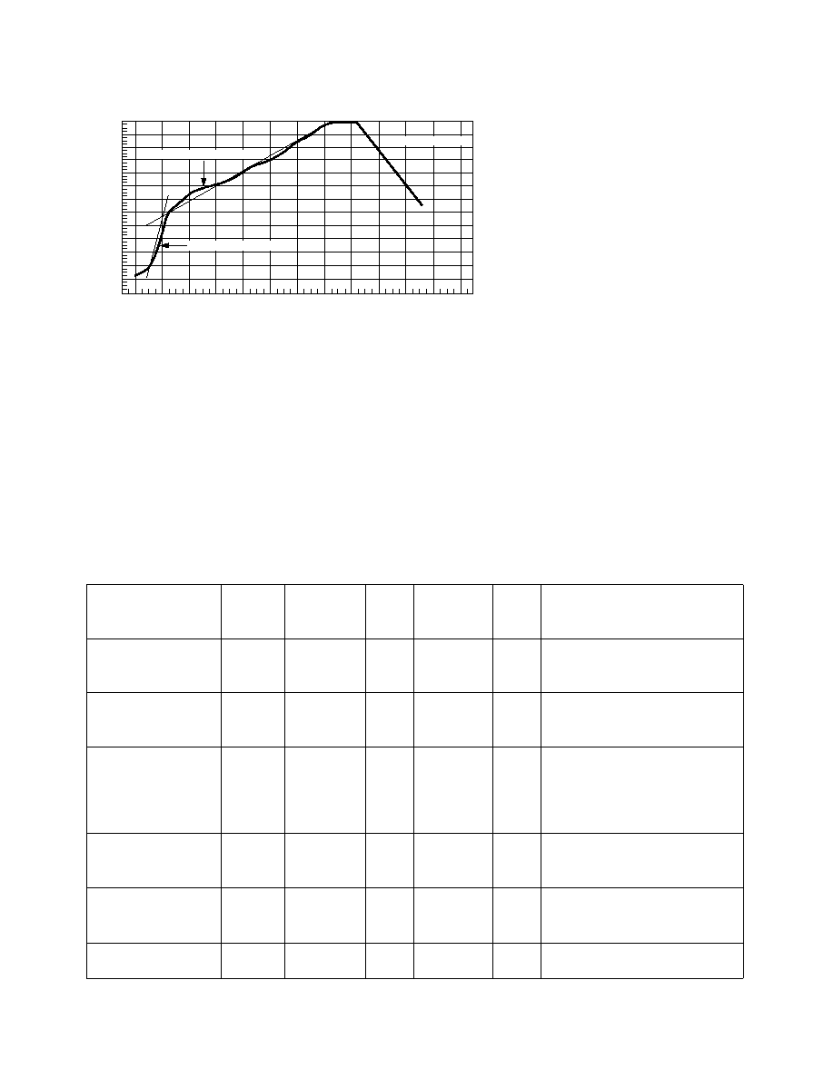
240
T = 115∞C, 0.3∞C/SEC
0
T = 100∞C, 1.5∞C/SEC
T = 145∞C, 1∞C/SEC
TIME ≠ MINUTES
TEMPERATURE ≠ ∞C
220
200
180
160
140
120
100
80
60
40
20
0
260
1
2
3
4
5
6
7
8
9
10
11
12
Solder Reflow Temperature Profile
1-53
VDE 0884 Insulation Related Characteristics
(HCPL-4506 OPTION 060 ONLY)
Description
Symbol
Characteristic
Units
Installation classification per DIN VDE 0110/1.89, Table 1
for rated mains voltage
300 V rms
I-IV
for rated mains voltage
450 V rms
I-III
Climatic Classification
55/100/21
Pollution Degree (DIN VDE 0110/1.89)
2
Maximum Working Insulation Voltage
V
IORM
630
V
peak
Input to Output Test Voltage, Method b*
V
IORM
x 1.875 = V
PR
, 100% Production Test with t
m
= 1 sec,
V
PR
1181
V
peak
Partial Discharge < 5 pC
Input to Output Test Voltage, Method a*
V
IORM
x 1.5 = V
PR
, Type and sample test,
V
PR
945
V
peak
t
m
= 60 sec, Partial Discharge < 5 pC
Highest Allowable Overvoltage*
(Transient Overvoltage, t
ini
= 10 sec)
V
IOTM
6000
V
peak
Safety Limiting Values
(Maximum values allowed in the event of a failure,
also see Figure 18, Thermal Derating curve.)
Case Temperature
T
S
175
∞
C
Input Current
I
S,INPUT
230
mA
Output Power
P
S,OUTPUT
600
mW
Insulation Resistance at T
S
, V
IO
= 500 V
R
S
10
9
VDE 0884 Insulation Related Characteristics (HCNW4506 ONLY)
Description
Symbol
Characteristic
Units
Installation classification per DIN VDE 0110/1.89, Table 1
for rated mains voltage
600 V rms
I-IV
for rated mains voltage
1000 V rms
I-III
Climatic Classification
55/100/21
Pollution Degree (DIN VDE 0110/1.89)
2
Maximum Working Insulation Voltage
V
IORM
1414
V
peak
Input to Output Test Voltage, Method b*
V
IORM
x 1.875 = V
PR
, 100% Production Test with t
m
= 1 sec,
V
PR
2652
V
peak
Partial Discharge < 5 pC
Input to Output Test Voltage, Method a*
V
IORM
x 1.5 = V
PR
, Type and sample test,
V
PR
2121
V
peak
t
m
= 60 sec, Partial Discharge < 5 pC
Highest Allowable Overvoltage*
(Transient Overvoltage, t
ini
= 10 sec)
V
IOTM
8000
V
peak
Safety Limiting Values
(Maximum values allowed in the event of a failure,
also see Figure 18, Thermal Derating curve.)
Case Temperature
T
S
150
∞
C
Input Current
I
S,INPUT
400
mA
Output Power
P
S,OUTPUT
700
mW
Insulation Resistance at T
S
, V
IO
= 500 V
R
S
10
9
*Refer to the front of the optocoupler section of the current catalog, under Product Safety Regulations section (VDE 0884), for a
detailed description.
Note: Isolation characteristics are guaranteed only within the safety maximum ratings which must be ensured by protective circuits in
application.