
Seven Segment Displays for High
Light Ambient Conditions
Technical Data
Features
∑ High Light Output
Typical Intensities of Up to 7.0
mcd/seg at 100 mA pk 1 of 5
Duty Factor
∑ Capable of High Current
Drive
Excellent for Long Digit String
Multiplexing
∑ Four Character Sizes
7.6 mm, 10.9 mm, 14.2 mm,
and 20.3 mm
∑ Choice of Two Colors
High Efficiency Red
Yellow
∑ Excellent Character
Appearance
Evenly Lighted Segments
Wide Viewing Angle
Gray Body for Optimum
Contrast
∑ Categorized for Luminous
Intensity; Yellow
Categorized for Color
Use of Like Categories Yields a
Uniform Display
∑ IC Compatible
∑ Mechanically Rugged
Description
The HDSP-3530/-3730/-5530/
-3900 and HDSP-4030/-4130/
-5730/-4200 are 7.6 mm, 10.9
mm/14.2 mm/20.3 mm high
efficiency red and yellow displays
designed for use in high light
ambient condition. The four sizes
of displays allow for viewing
distances at 3, 6, 7, and 10
meters. These seven segment
displays utilize large junction
high efficiency LED chips made
from GaAsP on a transparent GaP
substrate. Due to the large
junction area, these displays can
be driven at high peak current
levels needed for high ambient
conditions or many character
multiplexed operation.
These displays have industry
standard packages, and pin
configurations and
±
1 overflow
display are available in all four
sizes. These numeric displays are
ideal for applications such as
Automotive and Avionic
Instrumentation, Point of Sale
Terminals, and Gas Pump.
High Efficiency Red
HDSP-3530/-3730/-5530/
-3900 Series
Yellow
HDSP-4030/-4130/-5730/
-4200 Series
2
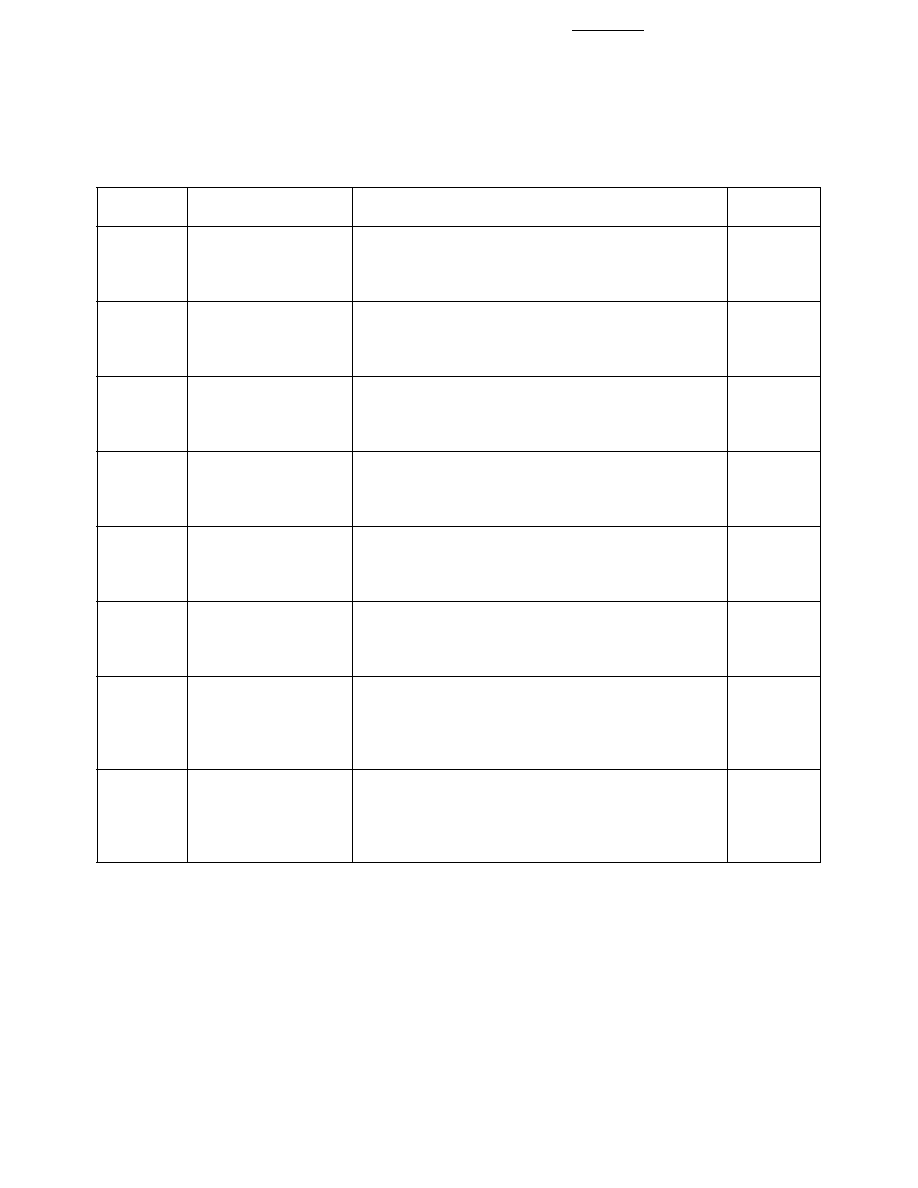
Devices
Part No.
Package
HDSP-
Color
Description
Drawing
3530
High Efficiency Red
7.6 mm Common Anode Left Hand Decimal
A
3531
7.6 mm Common Anode Right Hand Decimal
B
3533
7.6 mm Common Cathode Right Hand Decimal
C
3536
7.6 mm Universal Overflow
±
1 Right Hand Decimal
D
4030
Yellow
7.6 mm Common Anode Left Hand Decimal
A
4031
7.6 mm Common Anode Right Hand Decimal
B
4033
7.6 mm Common Cathode Right Hand Decimal
C
4036
7.6 mm Universal Overflow
±
1 Right Hand Decimal
D
3730
High Efficiency Red
10.9 mm Common Anode Left Hand Decimal
E
3731
10.9 mm Common Anode Right Hand Decimal
F
3733
10.9 mm Common Cathode Right Hand Decimal
G
3736
10.9 mm Universal Overflow
±
1 Right Hand Decimal
H
4130
Yellow
10.9 mm Common Anode Left Hand Decimal
E
4131
10.9 mm Common Anode Right Hand Decimal
F
4133
10.9 mm Common Cathode Right Hand Decimal
G
4136
10.9 mm Universal Overflow
±
1 Right Hand Decimal
H
5531
High Efficiency Red
14.2 mm Common Anode Right Hand Decimal
I
5533
14.2 mm Common Cathode Right Hand Decimal
J
5537
14.2 mm Overflow
±
1 Common Anode
K
5538
14.1 mm Overflow
±
1 Common Cathode
L
5731
Yellow
14.2 mm Common Anode Right Hand Decimal
I
5733
14.2 mm Common Cathode Right Hand Decimal
J
5737
14.2 mm Overflow
±
1 Common Anode
K
5738
14.1 mm Overflow
±
1 Common Cathode
L
3900
High Efficiency Red
20.3 mm Common Left Hand Decimal
M
3901
20.3 mm Common Anode Right Hand Decimal
N
3903
20.3 mm Common Cathode Right Hand Decimal
O
3905
20.3 mm Common Cathode Left Hand Decimal
P
3906
20.3 mm Universal Overflow
±
1 Right Hand Decimal
Q
4200
Yellow
20.3 mm Common Left Hand Decimal
M
4201
20.3 mm Common Anode Right Hand Decimal
N
4203
20.3 mm Common Cathode Right Hand Decimal
O
4205
20.3 mm Common Cathode Left Hand Decimal
P
4206
20.3 mm Universal Overflow
±
1 Right Hand Decimal
Q
Note: Universal pinout brings the anode and cathode of each segment's LED out to separate pins. See internal diagrams D and H.
Absolute Maximum Ratings (All Products)
Average Power per Segment or DP (T
A
= 25
∞
C) ................................................................................. 105 mW
Peak Forward Current per Segment or DP (T
A
= 25
∞
C) ............................... 135 mA (Pulse Width = 0.16 ms)
DC Forward Current per Segment
[2]
or DP (T
A
= 25
∞
C) ........................................................................ 40 mA
Operating Temperature Range ................................................................................................. - 40
∞
C to +85
∞
C
Storage Temperature Range .................................................................................................... - 40
∞
C to +85
∞
C
Reverse Voltage per Segment or DP ........................................................................................................ 5.0 V
Lead Solder Temperature (1.59 mm [1/16 inch] below seating plane) .................................... 260
∞
C for 3 sec
Notes:
1. See Figure 1 to establish pulsed operating conditions
2. Derate maximum DC current above T
A
= 25
∞
C at 0.50 mA/
∞
C per segment, see Figure 2.


