1-37
H
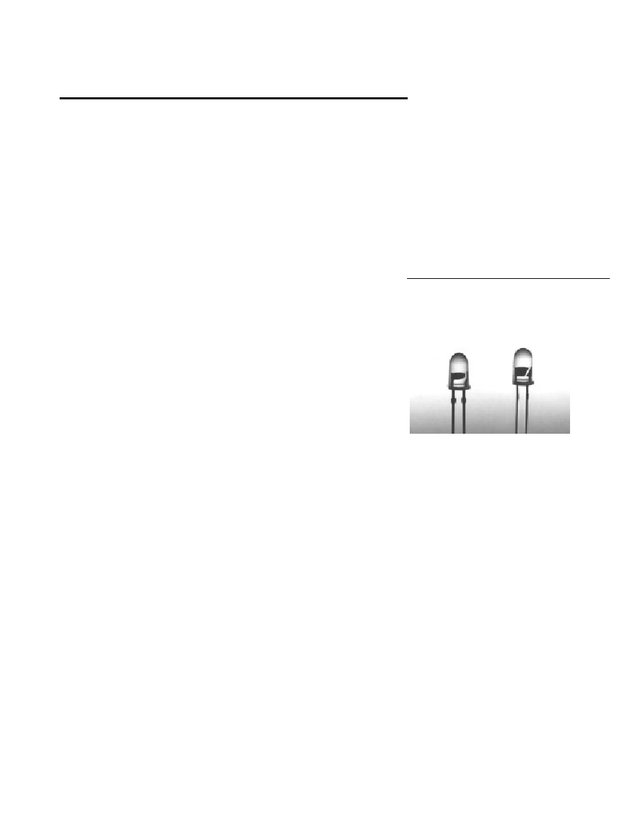
Description
These untinted, non-diffused, solid
state lamps utilize the latest
absorbing/transparent substrate
aluminum indium gallium phos-
phide (AS/TS AlInGaP) LED tech-
nology. These materials have a very
high luminous efficiency, capable
of producing high light output over
a wide range of drive currents. In
addition, these LED lamps are at
wavelengths ranging from amber
to reddish orange and at viewing
angles ranging from 7 to 45
degrees.
Features
· Outstanding LED Material
Efficiency
· High Light Output over a
Wide Range of Currents
· Low Electrical Power
Dissipation
· CMOS/MOS Compatible
· Colors: 590/592 nm Amber,
615/617 nm and 622 nm
Reddish-Orange
· Variety of Packages Available
Applications
· Outdoor Message Boards
· Safety Lighting Equipment
· Signaling Applications
· Emitter for Emitter/
Detector Applications
· Changeable Message Signs
· Portable Equipment
· Medical Equipment
· Automotive Lighting
· Alternative to Incandescent
Lamps
SunPower Series
HLMA-CX00 Series
HLMA-DX00 Series
HLMA-KX00 Series
HLMT-CX00 Series
HLMT-DX00 Series
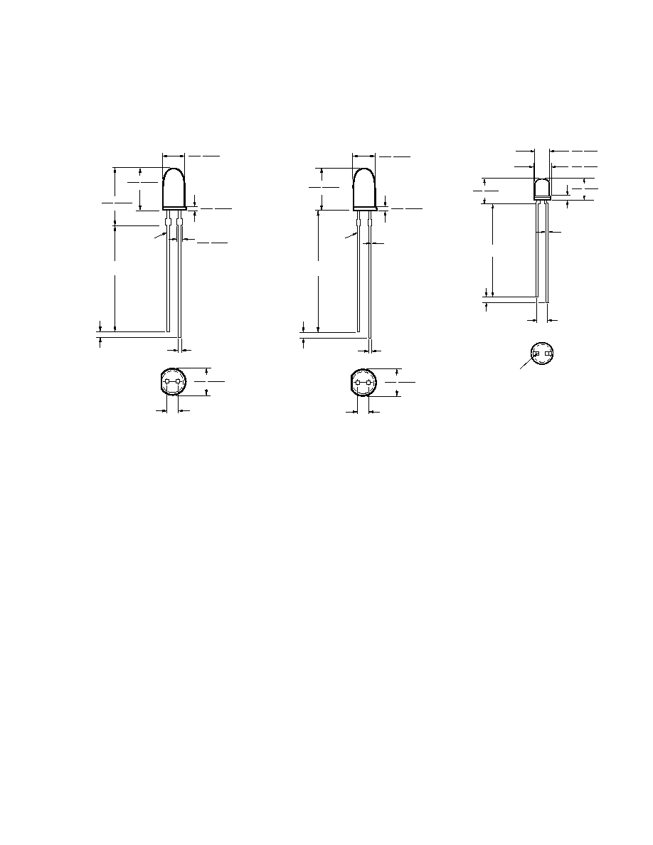
T-1
3
/
4
(5 mm), T-1 (3 mm), High
Performance AlInGaP LED
Lamps
Technical Data
5963-2323E

1-39
Absolute Maximum Ratings at T
A
= 25
°
C
(T-1
3
/
4
Package)
DC Forward Current
[1,4,5]
........................................................... 50 mA
Peak Forward Current
[2]
........................................................... 200 mA
Time Average Input Power
[2]
................................................... 103 mW
Transient Forward Current
[3]
(10
µ
s Pulse) .............................. 500 mA
Reverse Voltage (I
R
= 100
µ
A) ......................................................... 5 V
Operating Temperature Range .......................................... -40 to 100
°
C
Storage Temperature ......................................................... -40 to 120
°
C
Junction Temperature ................................................................. 130
°
C
Soldering Temperature .......................................... 260
°
C for 5 seconds
[1.59 mm (0.06 in.) below seating plane]
Notes:
1. Derate linearly as shown in Figure 4.
2. Any pulsed operation cannot exceed the Absolute Max Peak Forward Current or the
Max Allowable Time Average Power as specified in Figure 5.
3. The transient peak current is the maximum nonrecurring peak current the device can
withstand without damaging the LED die and wire bonds.
4. Drive Currents between 10 and 30 mA are recommended for best long term
performance.
5. Operation at currents below 10 mA is not recommended, please contact your
Hewlett-Packard sales representative.
Absolute Maximum Ratings at T
A
= 25
°
C
(T-1 Package)
DC Forward Current
[1,4,5]
........................................................... 50 mA
Peak Forward Current
[2]
........................................................... 200 mA
Time Average Input Power
[2]
................................................... 103 mW
Transient Forward Current
[3]
(10
µ
s Pulse) .............................. 500 mA
Reverse Voltage (I
R
= 100
µ
A) ......................................................... 5 V
Operating Temperature Range .......................................... -40 to 100
°
C
Storage Temperature ......................................................... -40 to 100
°
C
Junction Temperature .................................................................. 110
°
C
Solder Temperature ................................................ 260
°
C for 5 seconds
[1.59 mm (0.06 in.) below seating plane]
Notes:
1. Derate linearly as shown in Figure 4.
2. Any pulsed operation cannot exceed the Absolute Max Peak Forward Current or the
Max Allowable Time Average Power as specified in Figure 5.
3. The transient peak current is the maximum nonrecurring peak current the device can
withstand without damaging the LED die and wire bonds.
4. Drive Currents between 10 mA and 30 mA are recommended for best long term
performance.
5. Operation at currents below 10 mA is not recommended, please contact your
Hewlett-Packard sales representative.
1-40
Optical Characteristics at T
A
= 25
°
C
TS-AlInGaP T-1
3
/
4
Luminous
Color,
Intensity
Peak
Dominant
Viewing Angle
Luminous
Part
I
V
(mcd)
Wavelength
Wavelength
2
1
/
2
Efficacy
Number
@ 20 mA
[1]
peak
(nm)
d
[2]
(nm)
Degrees
[3]
v
Package
HLMT-
Min.
Typ.
Typ.
Typ.
Typ.
(lm/w)
Drawing
CL00
[1]
2600 8300
594
592
8
480
A
CH00
[1]
2900 9000
623
617
8
263
DL00
[4]
450
1500
594
592
24
480
B
DH00
[4]
500
1800
623
617
24
263
AS-AlInGaP T-1
Luminous
Color,
Intensity
Peak
Dominant
Viewing Angle
Luminous
Part
I
V
(mcd)
Wavelength
Wavelength
2
1
/
2
Efficacy
Number
@ 20 mA
[1]
peak
(nm)
d
[2]
(nm)
Degrees
[3]
v
Package
HLMA-
Min.
Typ.
Typ.
Typ.
Typ.
(lm/w)
Drawing
KL00
35
200
592
590
45
480
C
KH00
35
200
621
615
45
263
Notes:
1. The luminous intensity, I
v
, is measured at the mechanical axis of the lamp package. The actual peak of the spatial radiation pattern
may not be aligned with this axis.
2. The dominant wavelength,
d
, is derived from the CIE Chromaticity Diagram and represents the color of the device.
3.
1/2
is the off-axis angle where the luminous intensity is 1/2 the peak intensity.
Notes:
1. The luminous intensity, I
V
, is measured at the peak of the spatial radiation pattern which may not be aligned with the mechanical axis
of the lamp package.
2. The dominant wavelength,
d
, is derived from the CIE Chromaticity Diagram and represents the color of the device.
3.
1/2
is the off-axis angle where the luminous intensity is 1/2 the peak intensity.
4. The luminous intensity, I
v
, is measured at the mechanical axis of the lamp package. The actual peak of the spatial radiation pattern
may not be aligned with this axis.
AS-AlInGaP T-1
3
/
4
Luminous
Color,
Intensity
Peak
Dominant
Viewing Angle
Luminous
Part
I
V
(mcd)
Wavelength
Wavelength
2
1
/
2
Efficacy
Number
@ 20 mA
[1]
peak
(nm)
d
[2]
(nm)
Degrees
[3]
v
Package
HLMA-
Min.
Typ.
Typ.
Typ.
Typ.
(lm/w)
Drawing
CL00
[1]
1000 3500
592
590
7
480
A
CH00
[1]
1000 3500
621
615
7
263
DL00
[4]
300 800
592
590
24
480
B
DH00
[4]
290
600
621
615
24
263
DG00
[4]
290 500
630
622
24
197
Notes:
1. The luminous intensity, I
V
, is measured at the peak of the spatial radiation pattern which may not be aligned with the mechanical axis
of the lamp package.
2. The dominant wavelength,
d
, is derived from the CIE Chromaticity Diagram and represents the color of the device.
3.
1/2
is the off-axis angle where the luminous intensity is 1/2 the peak intensity.
4. The luminous intensity, I
v
, is measured at the mechanical axis of the lamp package. The actual peak of the spatial radiation pattern
may not be aligned with this axis.