 | –≠–ª–µ–∫—Ç—Ä–æ–Ω–Ω—ã–π –∫–æ–º–ø–æ–Ω–µ–Ω—Ç: HLMP-4101 | –°–∫–∞—á–∞—Ç—å:  PDF PDF  ZIP ZIP |

Agilent HLMP-4100/4101
T-1
3
/
4
(5 mm)
Double Heterojunction AlGaAs
Very High Intensity Red LED Lamps
Data Sheet
Features
∑ 1000 mcd at 20 mA
∑ Very high intensity at low drive
currents
∑ Narrow viewing angle
∑ Outstanding material efficiency
∑ Low forward voltage
∑ CMOS/MOS compatible
∑ TTL compatible
∑ Deep red color
Applications
∑ Bright ambient lighting conditions
∑ Emitter/detector and signaling
applications
∑ General use
Description
These solid state LED lamps
utilize newly developed double
heterojunction (DH) AlGaAs/GaAs
material technology. This LED
material has outstanding light
output efficiency over a wide range
of drive currents. The lamp package
has a tapered lens designed to
concentrate the luminous flux
into a narrow radiation pattern to
achieve a very high intensity. The
LED color is deep red at the
dominant wavelength of 637
nanometers. These lamps may be
DC or pulse driven to achieve
desired light output.
Package Dimensions
6.10 (0.240)
5.59 (0.220)
2.54 (0.100)
NOMINAL
CATHODE
23.0 (0.90) MIN.
12.44 (0.490)
11.68 (0.460)
9.19 (0.362)
8.43 (0.332)
1.32 (0.052)
1.02 (0.040)
0.64 (0.025)
SQUARE
NOMINAL
0.89 (0.035)
0.64 (0.025)
1.27 (0.050) NOM.
5.08 (0.200)
4.57 (0.180)

2
Note:
1.
1
/
2
is the angle from optical centerline where the luminous intensity is
1
/
2
the optical
centerline value.
Selection Guide
Luminous Intensity Iv (mcd) at 20 mA
2
1/2
[1]
Device HLMP-
Min.
Typ.
Max.
Degree
4100
500.0
750.0
≠
8
4101
700.0
1000.0
≠
8
4101-ST0xx
1400.0
2700.0
4000.0
8
Part Numbering System
Notes:
1. `0' indicates no maximum intensity limit.
2. `0' indicates full color distribution.
HLMX
-
4
1
XX
-
X
X
X
XX
Mechanical Option
00: Bulk
Color Bin Options
0: Full color bin distribution
Maximum Iv Bin Options
0: Open (No. max. limit)
Others: Please refer to the Iv bin Table
Minimum Iv Bin Options
Please refer to the Iv bin Table
Brightness Level
00: Lower brightness
01: Higher brightness

3
Absolute Maximum Ratings at T
A
= 25
∞
C
Parameter
Maximum Rating
Units
Peak Forward Current
[1, 2]
300
mA
Average Forward Current
[2]
20
mA
DC Current
[3]
30
mA
Power Dissipation
87
mW
Reverse Voltage (I
R
= 100
µ
A)
5
V
Transient Forward Current (10
µ
s Pulse)
[4]
500
mA
Operating Temperature Range
-20 to +100
∞
C
Storage Temperature Range
-55 to +100
∞
C
Wave Soldering Temperature [1.59 mm (0.063 in.) from body]
250
∞
C for 3 seconds
Lead Solder Dipping Temperature [1.59 mm (0.063 in.) from body]
260
∞
C for 5 seconds
Notes:
1. Maximum I
PEAK
at f = 1 kHz, DF = 6.7%.
2. Refer to Figure 6 to establish pulsed operating conditions.
3. Derate linerally as shown in Figure 5.
4. The transient peak current is the maximum non-recurring peak current the device can withstand without damaging the LED die and wire bonds. It
is not recommended that the device be operated at peak currents beyond the Absolute Maximum Peak Forward Current.
Electrical/Optical Characteristics at T
A
= 25
∞
C
Symbol
Description
Min.
Typ.
Max.
Unit
Test Condition
V
F
Forward Voltage
1.8
2.2
V
20 mA
V
R
Reverse Breakdown Voltage
5.0
15.0
V
I
R
= 100
µ
A
PEAK
Peak Wavelength
650
nm
Measurement at peak
d
Dominant Wavelength
642
nm
Note 1
1
/
2
Spectral Line Halfwidth
20
nm
s
Speed of Response
30
ns
Exponential Time
Constant, e
-t/2
C
Capacitance
30
pF
V
F
= 0, f = 1 MHz
jc
Thermal Resistance
220
∞
C/W
Junction to Cathode Lead
v
Luminous Efficacy
80
1 m/W
Note 2
Notes:
1. The dominant wavelength,
d, is derived from the CIE chromaticity diagram and represents the color of the device.
2. The radiant intensity, Ie, in watts per steradian, may be found from the equation Ie = Iv/
v, where Iv is the luminous intensity in candelas and
v is
luminous efficacy in lumens/watt.
3. The approximate total luminous flux output within a cone angle of 2
about the optical axis,
v(2
), may be obtained from the following formula:
v(2
) = [
v(
)/Iv(0)]Iv; Where:
v(
)/Iv(0) is obtained from Figure 7.
4
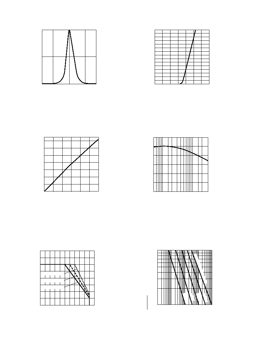
Figure 1. Relative intensity vs. wavelength.
Figure 2. Forward current vs. forward voltage.
Figure 3. Relative luminous intensity vs. dc forward current.
Figure 4. Relative efficiency vs. peak forward current.
Figure 5. Maximum forward dc current vs. ambient temperature
derating based on T
J
MAX. = 110
∞
C.
Figure 6. Maximum tolerable peak current vs. peak duration (I
PEAK
MAX. determined from temperature derated I
DC
MAX.).
RELATIVE INTENSITY
0
0
WAVELENGTH ≠ nm
700
1.0
0.5
650
600
I F
≠
FORWARD CURRENT
≠
mA
0
0
VF ≠ FORWARD VOLTAGE ≠ V
3.0
300
2.0
0.5
1.0
1.5
2.5
3.5
280
260
240
220
200
180
160
140
120
100
80
60
40
20
NORMALIZED LUMINOUS INTENSITY
(NORMALIZED AT 20 mA)
0
0
IDC ≠ DC FORWARD CURRENT ≠ mA
30
20
5
10
15
25
1.4
1.2
1.0
0.8
0.6
0.4
0.2
V
≠
RELATIVE EFFICIENCY (NORMALIZED AT 20 mA)
5
0
IPEAK ≠ PEAK FORWARD CURRENT ≠ mA
100
10
20
50
200 300
1.2
1.0
0.8
0.6
0.4
0.2
I F
≠
FORWARD CURRENT
≠
mA
0
0
TA ≠ AMBIENT TEMPERATURE ≠
∞
C
90
20
70 80
100 110
40
35
30
25
20
15
10
5
60
50
40
30
10
R
J-A
= 559
∞
C/W
R
J-A
= 574
∞
C/W
R
J-A
= 689
∞
C/W
RATIO OF MAXIMUM PEAK CURRENT
TO TEMPERATURE DERATED
MAXIMUM DC CURRENT
I PEAK
MAX.
I DC
MAX.
tp ≠ PULSE DURATION ≠
µ
s
3
1
10
10
10000
1000
100
1
3 KHz
10 KHz
1 KHz
300 Hz
f
≠
REFRESH RATE
≠
100 Hz
2
9
8
7
6
5
4

5
Figure 7. Relative luminous intensity vs. angular displacement.
Note:
All categories are established for classification of products. Products may not be available in all
categories. Please contact your local Agilent representative for further clarification/information.
Mechanical Option Matrix
Mechanical Option Code
Definition
00
Bulk Packaging, minimum increment 500 pcs/bag
Intensity Bin Limits
Intensity Range (mcd)
Color
Bin
Min.
Max.
Red
P
540.0
850.0
Q
850.0
1200.0
R
1200.0
1700.0
S
1700.0
2400.0
T
2400.0
3400.0
U
3400.0
4900.0
V
4900.0
7100.0
W
7100.0
10200.0
X
10200.0
14800.0
Y
14800.0
21400.0
Z
21400.0
30900.0
Tolerance for each bin limit is
±
18%.
10
100
40
70
20
60
80
30
50
90
LUMINOUS FLUX TO INTENSITY RATIO
WITHIN A GIVEN CONE ANGLE
0
∞
10
∞
20
∞
30
∞
40
∞
50
∞
60
∞
70
∞
80
∞
90
∞
0
0.02
0.04
0.06
0.08
0.10
0.12
0.14
0.135
N
(
)
I V
(0)
≠ ANGLE FROM OPTICAL CENTERLINE ≠ DEGREES
(CONE HALF ANGLE)
NORMALIZED INTENSITY
0