 | –≠–ª–µ–∫—Ç—Ä–æ–Ω–Ω—ã–π –∫–æ–º–ø–æ–Ω–µ–Ω—Ç: HSMB-C190 | –°–∫–∞—á–∞—Ç—å:  PDF PDF  ZIP ZIP |

Surface Mount Chip LEDs
Technical Data
HSMB-C190/C170/
C110/C150
Features
∑ Small Size
∑ Industry Standard Footprint
∑ Compatible with IR Solder
∑ Diffused Optics
∑ Operating Temperature
Range of -30
∞
C to +85
∞
C
∑ Right Angle Package
Available
∑ SiC Blue Color
∑ Available in 8 mm tape on 7"
(178 mm) Diameter Reels
Applications
∑ Keypad Backlighting
∑ Push-Button Backlighting
∑ LCD Backlighting
∑ Symbol Backlighting
∑ Front Panel Indicator
Description
These Blue chip LEDs are
designed in an industry standard
package for ease of handling
and use. Blue color chip LED is a
new product that offers color
differentiation for backlighting
applications.
The HSMB-C150 has the industry
standard 3.2 x 1.6 mm footprint
that is excellent for all around use.
The HSMB-C170 has the widely
used 2.0 x 1.25 mm footprint. The
HSMB-C190 has the industry
standard 1.6 x 0.8 mm footprint,
its low 0.8 mm profile and wide
viewing angle make this LED
exceptional for backlighting
applications.
The HSMB-C110 is a right-angle
package with the universally
accepted dimensions of 3.2 x 1.0
Footprint (mm)
SiC Blue
Parts Per Reel
2.00 x 1.25
HSMB-C170
4000
1.60 x 0.80
HSMB-C190
4000
3.20 x 1.00
[1]
HSMB-C110
3000
3.20 x 1.60
HSMB-C150
3000
Note:
1. Right-angle package.
x 1.5 mm. This part is ideal for
LCD backlighting and sidelighting
applications.
All packages are compatible with
IR reflow solder processes. The
small size and wide viewing angle
make these LEDs prime choices
for backlighting applications and
front panel illumination especially
where space is a premium.
Device Selection Guide

2
Package Dimensions
HSMB-C190
HSMB-C170
HSMB-C110
1.6
(0.063 )
0.3 (0.012)
0.3 ± 0.15
(0.012 ± 0.006)
0.3 (0.012)
POLARITY
CATHODE
MARK
0.8 (0.031)
0.3 ± 0.15
(0.012 ± 0.006)
1.0
(0.039)
0.4 (0.016)
LED DIE
DIFFUSED EPOXY
PC BOARD
SOLDERING
TERMINAL
0.8 (0.031)
2.0 (0.079 )
0.3 (0.012)
0.4 ± 0.15
(0.016 ± 0.006)
0.3 (0.012)
POLARITY
CATHODE
MARK
0.8 (0.031)
0.4 ± 0.15
(0.016 ± 0.006)
1.4
(0.055)
0.62 (0.024)
LED DIE
DIFFUSED
EPOXY
PC BOARD
SOLDERING
TERMINAL
1.25 (0.049)
3.2 (0.126 )
0.5 (0.020)
1.0 (0.039)
POLARITY
CATHODE
MARK
1.5 (0.059)
LED DIE
CLEAR
EPOXY
PC BOARD
SOLDERING
TERMINAL
1.0 (0.039)
1.0 (0.039)
2.6 (0.102 )
1.6 (0.063 )
CATHODE LINE
NOTE:
1. ALL DIMENSIONS IN MILLIMETERS (INCHES).
2. TOLERANCE IS ± 0.1 mm (± 0.004 IN.) UNLESS OTHERWISE SPECIFIED.
3.2 (0.126 )
0.5 (0.020)
0.50 ± 0.2
(0.020 ± 0.008)
0.6 (0.024)
POLARITY
CATHODE
MARK
1.1 (0.043)
0.50 ± 0.2
(0.020 ± 0.008)
2.0 (0.079)
0.8 (0.031)
LED DIE
DIFFUSED
EPOXY
PC BOARD
SOLDERING
TERMINAL
1.6 (0.063)
HSMB-C150

3
Absolute Maximum Ratings at T
A
=25
∞
C
Parameter
HSMB-C190/C170/C110/C150
Units
DC Forward Current
[1]
20
mA
Peak Pulsing Current
[2]
100
mA
Power Dissipation
92
mW
Reverse Voltage (I
R
= 100
µ
A)
5
V
Maximum LED Junction Temperature
95
∞
C
Operating Temperature Range
-30 to +85
∞
C
Storage Temperature Range
-40 to +85
∞
C
Soldering Temperature
See IR soldering profile (Figure 7)
Notes:
1. Derate linearly as shown in Figure 4 for temperature above 25
∞
C.
2. Pulse condition of 1/10 duty and 0.1 msec. width.
Optical Characteristics at T
A
=25
∞
C
Luminous
Peak
Dominant
Viewing
Intensity
[1]
Wavelength
Wavelength
Angle 2
1/2
Part No.
Color
I
v
(mcd) @ 20 mA
peak
(nm)
d
(nm)
(degrees)
[2]
Min.
Typ.
Typ.
Typ.
Typ.
HSMB-
SiC Blue
1.60
6.0
428
466
170
C190/C170/C150
HSMB-C110
SiC Blue
1.60
6.5
428
466
130
Notes:
1. The luminous intensity, I
v
, is measured at the peak of the spatial radiation pattern, which may not be aligned with the mechanical
axis of the lamp package.
2.
1/2
is the off-axis angle where the luminous intensity is 1/2 the peak intensity.
Electrical Characteristics at T
A
=25
∞
C
Reverse
Forward Voltage
Breakdown
Thermal
Capacitance C
V
F
(Volts)
V
R
(Volts)
Resistance
(pF) @ V
F
= 0 V,
Part No.
@ I
F
= 20 mA
@ I
R
= 100
µ
A
R
J-P
(
∞
C/W)
f = 1 MHz
Typ.
Max.
Min.
Typ.
Typ.
HSMB-C190/C170/C150
3.8
4.6
5
300
67
HSMB-C110
3.8
4.6
5
300
67

4
Figure 1. Relative Intensity vs.
Wavelength.
Figure 3. Relative Luminous Intensity
vs. Forward Current.
Figure 4. Maximum Forward Current
vs. Ambient Temperature.
Figure 5. Relative Intensity vs. Angle for HSMB-C110.
Figure 2. Forward Current vs.
Forward Voltage.
100
10
1
0.1
3.0
3.2
3.6
3.8
4.0
VF ≠ FORWARD VOLTAGE ≠ V
I F
≠ FORWARD CURRENT ≠ mA
3.4
0
5
15
25
IF ≠ FORWARD CURRENT ≠ mA
0
0.4
1.0
1.2
RELATIVE LUMINOUS INTENSITY
(NORMALIZED AT 20 mA)
20
0.6
0.2
0.8
10
0
25
0
20
60
80
100
5
I F MAX.
≠ MAXIMUM FORWARD CURRENT ≠ mA
TA ≠ AMBIENT TEMPERATURE ≠ ∞C
40
15
10
20
380
100
0
580
680
20
RELATIVE INTENSITY ≠ %
WAVELENGTH ≠ nm
480
60
40
80
RELATIVE INTENSITY ≠ %
100
0
ANGLE
80
60
50
70
20
10
30
40
90
-70
-50
-30
0
20 30
50
70
90
-90
-20
-80
-60
-40
-10
10
40
60
80
RELATIVE INTENSITY ≠ %
100
0
ANGLE
80
60
50
70
20
10
30
40
90
-70
-50
-30
0
20 30
50
70
90
-90
-20
-80
-60
-40
-10
10
40
60
80
5
Figure 6. Relative Intensity vs. Angle for HSMB-C170, HSMB-C190, and
HSMB-C150.
Figure 8. Recommended Soldering Pattern for
HSMB-C170.
Figure 9. Recommended Soldering Pattern for
HSMB-C190.
Figure 10. Recommended Soldering Pattern for
HSMB-C110.
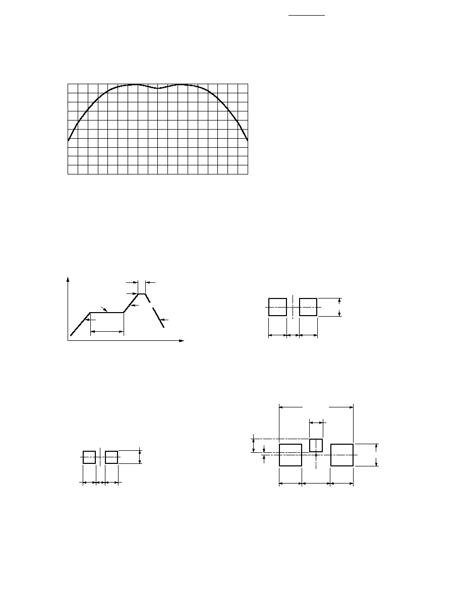
Figure 7. Recommended Reflow Soldering Profile.
Note:
1. All dimensions in millimeters (inches).
230∞C MAX.
10 SEC. MAX.
4∞C/SEC.
MAX.
OVER 2 MIN.
TIME
TEMPERATURE
4∞C/SEC. MAX.
140-160∞C
≠3∞C/SEC. MAX.
1.2 (0.047)
1.2
(0.047)
0.9
(0.035)
1.2
(0.047)
0.8 (0.031)
0.8
(0.031)
0.7
(0.028)
0.8
(0.031)
5.0 (0.200)
1.5 (0.059)
1.5
(0.059)
1.5
(0.059)
2.0
(0.079)
0.9 (0.035)
0.2 (0.008)
0.9 (0.035)
RELATIVE INTENSITY ≠ %
100
0
ANGLE
80
60
50
70
20
10
30
40
90
-70
-50
-30
0
20 30
50
70
90
-90
-20
-80
-60
-40
-10
10
40
60
80