 | –≠–ª–µ–∫—Ç—Ä–æ–Ω–Ω—ã–π –∫–æ–º–ø–æ–Ω–µ–Ω—Ç: HSMP-3892 | –°–∫–∞—á–∞—Ç—å:  PDF PDF  ZIP ZIP |
Document Outline
- HSMP-38XX, -48XX Series
- Features
- Description/Applications
- Package Lead Code Identification
- Absolute Maximum Ratings
- Electrical Specifications
- Typical Specifications
- Typical Parameters
- Equivalent Circuit Model
- Typical Applications
- Microstrip Series Connection
- Microstrip Shunt Connections
- Package Dimensions
- PC Board Footprints
- Package Characteristics
- Profile Option Descriptions
- Ordering Information

Surface Mount PIN Diodes
Technical Data
Features
∑ Diodes Optimized for:
Low Current Switching
Low Distortion Attenuating
Ultra-Low Distortion
Switching
Microwave Frequency
Operation
∑ Surface Mount SOT-23 and
SOT-143 Packages
Single and Dual Versions
Tape and Reel Options
Available
∑ Low Failure in Time (FIT)
Rate
[1]
Note:
1. For more information see the
Surface Mount PIN Reliability Data
Sheet.
HSMP-38XX and
HSMP-48XX Series
Package Lead Code
Identification
COMMON
CATHODE
#4
UNCONNECTED
PAIR
#5
COMMON
ANODE
#3
SERIES
#2
SINGLE
#0
DUAL ANODE
#A
DUAL CATHODE
#B
required. The HSMP-48XX series
are special products featuring
ultra low parasitic inductance in
the SOT-23 package, specifically
designed for use at frequencies
which are much higher than the
upper limit for conventional
SOT-23 PIN diodes. The
HSMP-4810 diode is a low distor-
tion attenuating PIN designed for
operation to 3 GHz. The
HSMP-4820 diode is ideal for
limiting and low inductance
switching applications up to
1.5 GHz. The HSMP-4890 is
optimized for low current switch-
ing applications up to 3 GHz.
The HSMP-386X series of general
purpose PIN diodes are designed
for two classes of applications.
The first is attenuators where
current consumption is the most
important design consideration.
The second application for this
series of diodes is in switches
where low cost is the driving
issue for the designer.
The HSMP-386X series Total
Capacitance (C
T
) and Total
Resistance (R
T
) are typical
specifications. For applications
that require guaranteed perfor-
mance, the general purpose
HSMP-383X series is recom-
mended. For low distortion
Description/Applications
The HSMP-380X and HSMP-381X
series are specifically designed for
low distortion attenuator applica-
tions. The HSMP-382X series is
optimized for switching applica-
tions where ultra-low resistance is
required. The HSMP-3880 switch-
ing diode is an ultra low distortion
device optimized for higher power
applications from 50 MHz to
1.5 GHz. The HSMP-389X series is
optimized for switching applica-
tions where low resistance at low
current and low capacitance are
attenuators, the HSMP-380X or
-381X series are recommended.
For high performance switching
applications, the HSMP-389X
series is recommended.
A SPICE model is not available
for PIN diodes as SPICE does not
provide for a key PIN diode
characteristic, carrier lifetime.

2
Absolute Maximum Ratings
[1]
T
A
= 25
∞
C
Symbol
Parameter
Units
Absolute Maximum
I
f
Forward Current (1 ms Pulse)
Amp
1
P
t
Total Device Dissipation
mW
[2]
250
P
iv
Peak Inverse Voltage
--
Same as V
BR
T
j
Junction Temperature
∞
C
150
T
STG
Storage Temperature
∞
C
-65 to 150
Notes:
1. Operation in excess of any one of these conditions may result in permanent damage to
this device.
2. CW Power Dissipation at T
LEAD
= 25
∞
C. Derate to zero at maximum rated temperature.
PIN Switching Diodes
Electrical Specifications T
A
= 25
∞
C
Nearest
Maximum
Equivalent
Minimum
Maximum
Maximum
Shunt Mode
Part
Package
Axial Lead
Breakdown
Series
Total
Harmonic
Number
Marking
Lead
Part No.
Voltage
Resistance
Capacitance
Distortion
HSMP-
Code
[1]
Code
Configuration
5082-
V
BR
(V)
R
S
(
)
C
T
(pF)
Hmd (dBc)
3820
F0
0
Single
3188
50
0.6*
0.8*
--
3822
F2
2
Series
3823
F3
3
Common Anode
3824
F4
4
Common Cathode
3880
S0
0
Single
--
100
6.5
0.40
≠55
3890
G0
0
Single
--
100
2.5
0.30**
--
3892
G2
2
Series
3893
G3
3
Common Anode
3894
G4
4
Common Cathode
3895
G5
5
Unconnected Pair
Test Conditions
V
R
= V
BR
I
F
= 5 mA
V
R
= 50 V
2 f
o,
Z
o
= 50 W
Measure
f = 100 MHz
f = 1 MHz
f
o
= 400 MHz
I
R
10
µ
A
I
F
= 10 mA*
V
R
= 20 V*
P
in
= +30 dBm
V
R
= 5 V**
0 V bias
Note:
1. Package marking code is white.
PIN Attenuator Diodes
Electrical Specifications T
A
= 25
∞
C (Each Diode)
Nearest
Equivalent
Minimum
Maximum
Maximum
Minimum
Maximum
Part
Package
Axial Lead Breakdown
Series
Total
High
Low
Number
Marking
Lead
Part No.
Voltage
Resistance
Capacitance
Resistance
Resistance
HSMP-
Code
[1]
Code
Configuration
5082-
V
BR
(V)
R
S
(
)
C
T
(pF)
R
H
(
)
R
L
(
)
3800
D0
0
Single
3080
100
2.0
0.37
1000
8
3802
D2
2
Series
3804
D4
4
Common Cathode
3810
E0
0
Single
3081
100
3.0
0.35
1500
10
3812
E2
2
Series
3813
E3
3
Common Anode
3814
E4
4
Common Cathode
Test Conditions
V
R
= V
BR
I
F
= 100 mA
V
R
= 50 V
I
F
= 0.01 mA
I
F
= 20 mA
Measure
f = 100 MHz
f = 1 MHz
f = 100 MHz
f= 100 MHz
I
R
10
µ
A

3
PIN General Purpose Diodes, Electrical Specifications T
A
= 25
∞
C
Nearest
Equivalent
Minimum
Maximum
Maximum
Part
Package
Axial Lead
Breakdown
Series
Total
Number
Marking
Lead
Part No.
Voltage
Resistance
Capacitance
HSMP-
Code
[1]
Code
Configuration
5082-
V
BR
(V)
R
S
(
)
C
T
(pF)
3830
K0
0
Single
3077
200
1.5
0.3
3832
K2
2
Series
3833
K3
3
Common Anode
3834
K4
4
Common Cathode
Test Conditions
V
R
= V
BR
I
F
= 100 mA
V
R
= 50 V
Measure
f = 100 MHz
f = 1 MHz
I
R
10 mA
High Frequency (Low Inductance, 500 MHz ≠ 3 GHz) PIN Diodes, Electrical Specifications T
A
= 25
∞
C
Minimum
Maximum
Typical
Maximum
Typical
Break-
Series
Total
Total
Total
Part
Package
down
Resis-
Capaci-
Capaci-
Induc-
Number
Marking
Lead
Config-
Voltage
tance
tance
tance
tance
Appli-
HSMP-
Code
Code
uration
V
BR
(V)
R
S
(
)
C
T
(pF)
C
T
(pF)
L
T
(nH)
cation
4810
EB
B
Dual
100
3.0
0.35
0.4
1.0
Attenu-
Cathode
ator
4820
FA
A
Dual Anode
50
0.6*
0.75*
1.0
1.0*
Limiter
4890
GA
A
Dual Anode
100
2.5**
0.33
0.375
1.0
Switch
V
R
= V
BR
I
F
= 100 mA
V
R
= 50 V
V
R
= 50 V
f = 500 MHz ≠
Measure
I
F
= 10 mA*
f = 1 MHz
f = 1 MHz
3 GHz
I
R
10
µ
A
I
F
= 5 mA**
V
R
= 20 V*
V
R
= 0 V
V
R
= 20 V*
PIN General Purpose Diodes, Typical Specifications T
A
= 25
∞
C
Code
Minimum
Typical Series
Typical Total
Part Number
Marking
Lead
Breakdown
Resistance
Capacitance
HSMP-
Code
[1]
Code
Configuration
Voltage V
BR
(V)
R
S
(
)
C
T
(pF)
3860
L0
0
Single
50
3.0/1.5*
0.20
3862
L2
2
Series
3863
L3
3
Common Anode
3864
L4
4
Common Cathode
Test Conditions
V
R
= V
BR
I
F
= 10 mA
V
R
= 50 V
Measure
f = 100 MHz
f = 1 MHz
I
R
10
µ
A
*I
F
= 100 mA
Typical Parameters at T
A
= 25
∞
C
Part Number
Series Resistance
Carrier Lifetime
Reverse Recovery Time
Total Capacitance
HSMP-
R
S
(
)
(ns)
T
rr
(ns)
C
T
(pF)
380X
55
1800
500
0.32 @ 50 V
381X
75
1500
300
0.27 @ 50 V
382X
1.5
70*
7
0.60 @ 20 V
383X
20
500
80
0.20 @ 50 V
388X
3.8
2500
550
0.30 @ 50 V
389X
3.8
200*
≠
0.20 @ 5 V
Test Conditions
I
F
= 1 mA
I
F
= 50 mA
V
R
= 10 V
f = 100 MHz
I
R
= 250 mA
I
F
= 20 mA
I
F
= 10 mA*
I
F
= 10 mA*
90% Recovery
I
R
= 6 mA*
Note:
1. Package marking code is white.
4
Typical Parameters at T
A
= 25
∞
C (unless otherwise noted), Single Diode
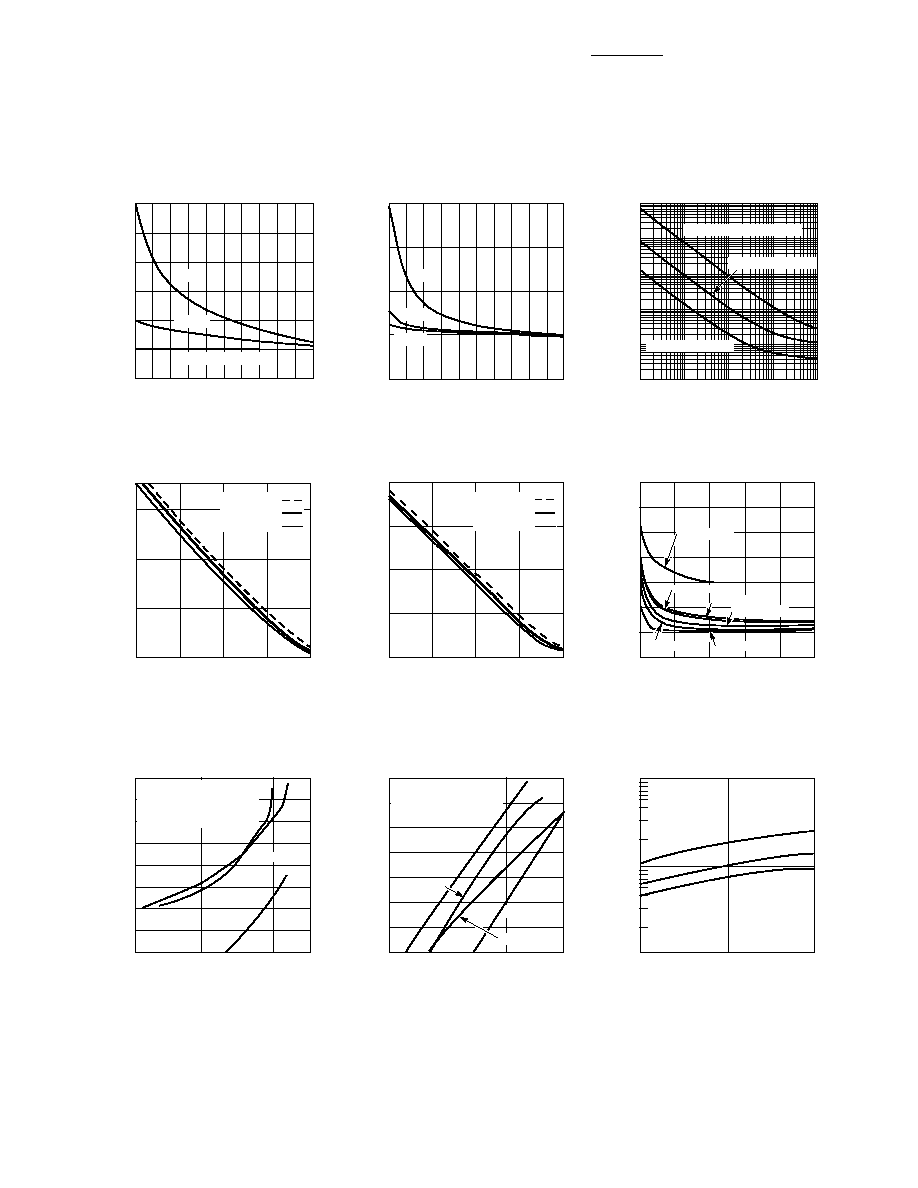
Figure 2. RF Capacitance vs. Reverse
Bias, HSMP-3830 Series.
0.15
0.30
0.25
0.20
0.35
0.40
0.45
0
2
6
4
10 12
8
16
14
18 20
TOTAL CAPACITANCE (pF)
REVERSE VOLTAGE (V)
Figure 1. RF Capacitance vs. Reverse
Bias, HSMP-3810 Series.
Figure 3. Resistance at 25
∞
C vs.
Forward Bias Current.
1 MHz
30 MHz
frequency>100 MHz
0.15
0.30
0.25
0.20
0.35
0
2
6
4
10 12
8
16
14
18 20
TOTAL CAPACITANCE (pF)
REVERSE VOLTAGE (V)
1 GHz
100 MHz
1 MHz
10000
1000
100
10
1
0.1
RESISTANCE (OHMS)
I
F
≠ FORWARD BIAS CURRENT (mA)
0.01
0.1
1
10
100
3000
1000
100
10
1
0.01
0.1
1
10
100
RF RESISTANCE (OHMS)
I
F
≠ FORWARD BIAS CURRENT (mA)
T
A
= +85
∞
C
T
A
= +25
∞
C
T
A
= ≠55
∞
C
10000
1000
100
10
1
RF RESISTANCE (OHMS)
0.01
0.1
1
10
100
I
F
≠ FORWARD BIAS CURRENT (mA)
T
A
= +85
∞
C
T
A
= +25
∞
C
T
A
= ≠55
∞
C
Figure 5. RF Resistance vs. Forward
Bias Current for HSMP-3810/
HSMP-4810.
1.4
1.2
1
0.8
0.6
0.4
0.2
0
0
10
20
30
40
50
V
R
≠ REVERSE VOLTAGE (V)
CAPACITANCE (pF)
HSMP-382X
HSMP-3880
HSMP-3800
HSMP-3890
HSMP-381X
HSMP-3830
Figure 6. Capacitance vs. Reverse
Voltage.
Figure 4. RF Resistance vs. Forward
Bias Current for HSMP-3800.
120
110
100
90
80
70
60
50
40
1000
100
10
Diode Mounted as a
Series Attenuator
in a 50 Ohm Microstrip
and Tested at 123 MHz
DIODE RF RESISTANCE (OHMS)
Figure 7. 2nd Harmonic Input
Intercept Point vs. Diode RF
Resistance for Attenuator Diodes.
INPUT INTERCEPT POINT (dBm)
HSMP-3810
HSMP-3830
HSMP-3830
120
115
110
105
100
95
90
85
1
10
30
I
F
≠ FORWARD BIAS CURRENT (mA)
Figure 8. 2nd Harmonic Input
Intercept Point vs. Forward Bias
Current for Switch Diodes.
INPUT INTERCEPT POINT (dBm)
HSMP-3880
HSMP-3820
HSMP-3880
HSMP-3830
HSMP-3890
Diode Mounted as a
Series Attenuator in a
50 Ohm Microstrip and
Tested at 123 MHz
FORWARD CURRENT (mA)
Figure 9. Reverse Recovery Time vs.
Forward Current for Various Reverse
Voltages. HSMP-3820 Series.
T
rr
≠ REVERSE RECOVERY TIME (ns)
1
10
100
10
20
30
V
R
= 2 V
V
R
= 5 V
V
R
= 10 V
HSMP-382X
HSMP-381x, /HSMP-4810
HSMP-382x, -4820
HSMP-383x, -386x
5
Typical Parameters
(continued)
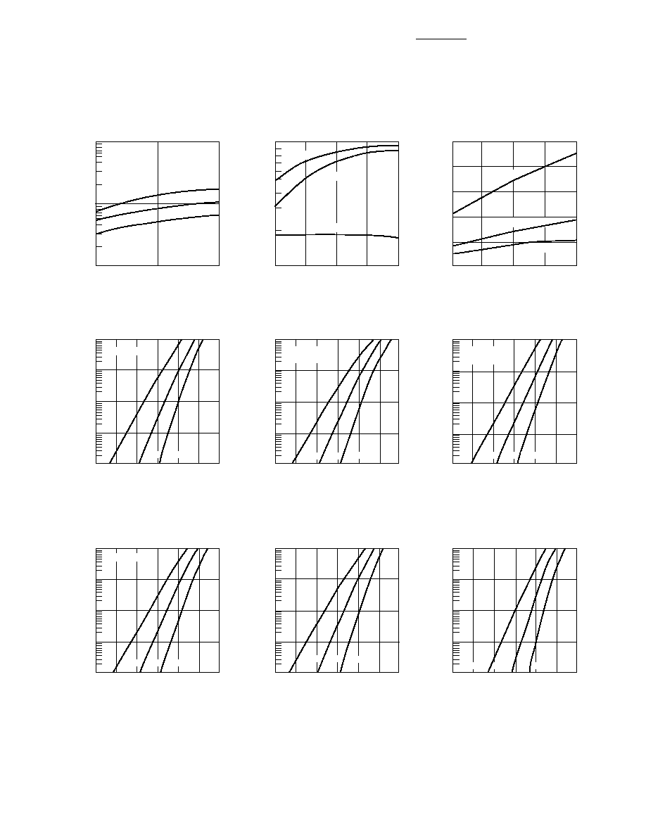
1000
100
10
10
20
30
T
rr
- REVERSE RECOVERY TIME (nS)
FORWARD CURRENT (mA)
Figure 10. Reverse Recovery Time vs.
Forward Current for Various Reverse
Voltage. HSMP-3830 Series.
HSMP-3830
V
R
= 5V
V
R
= 10V
V
R
= 20V
1000
900
800
400
100
10
20
25
15
30
REVERSE RECOVERY TIME (nS)
FORWARD CURRENT (mA)
Figure 11. Typical Reverse Recovery
Time vs. Reverse Voltage. HSMP-3880
Series.
700
600
500
200
300
V
R
= 5 V
V
R
= 10 V
V
R
= 20 V
200
160
120
80
40
0
10
20
15
25
30
T
RR
- REVERSE RECOVERY TIME (nS)
FORWARD CURRENT (mA)
Figure 12. Typical Reverse Recovery
Time vs. Reverse Voltage. HSMP-3890
Series.
V
R
= ≠2 V
V
R
= ≠5 V
V
R
= ≠10 V
100
10
1
0.1
0.01
0
0.2
0.4
0.6
0.8
1.0
1.2
I
F
≠ FORWARD CURRENT (mA)
V
F
≠ FORWARD VOLTAGE (mA)
Figure 13. Forward Current vs.
Forward Voltage. HSMP-3800 Series.
125
∞
C
25
∞
C ≠50
∞
C
HSMP-3800
100
10
1
0.1
0.01
0
0.2
0.4
0.6
0.8
1.0
1.2
I
F
≠ FORWARD CURRENT (mA)
V
F
≠ FORWARD VOLTAGE (mA)
Figure 14. Forward Current vs.
Forward Voltage. HSMP-3810 and
HSMP-4810 Series.
HSMP-3810
HSMP-4810
125
∞
C 25
∞
C ≠50
∞
C
100
10
1
0.1
0.01
0
0.2
0.4
0.6
0.8
1.0
1.2
I
F
≠ FORWARD CURRENT (mA)
V
F
≠ FORWARD VOLTAGE (mA)
Figure 15. Forward Current vs.
Forward Voltage. HSMP-3820 and
HSMP-4820 Series.
HSMP-382X
HSMP-482X
125
∞
C 25
∞
C ≠50
∞
C
100
10
1
0.1
0.01
0
0.2
0.4
0.6
0.8
1.0
1.2
I
F
≠ FORWARD CURRENT (mA)
V
F
≠ FORWARD VOLTAGE (mA)
Figure 16. Forward Current vs.
Forward Voltage. HSMP-3830 Series.
HSMP-3830
125
∞
C 25
∞
C ≠50
∞
C
100
10
1
0.1
0.01
0
0.2
0.4
0.6
0.8
1.0
1.2
I
F
≠ FORWARD CURRENT (mA)
V
F
≠ FORWARD CURRENT (mA)
Figure 17. Forward Current vs.
Forward Voltage. HSMP-3880 Series.
125
∞
C
25
∞
C ≠55
∞
C
100
10
1
0.1
0.01
0
0.2
0.4
0.6
0.8
1.0
1.2
I
F
≠ FORWARD CURRENT (mA)
V
F
≠ FORWARD VOLTAGE (mA)
Figure 18. Forward Current vs.
Forward Voltage. HSMP-3890 and
HSMP-4890 Series.
25
∞
C
125
∞
C
≠55
∞
C