 | –≠–ª–µ–∫—Ç—Ä–æ–Ω–Ω—ã–π –∫–æ–º–ø–æ–Ω–µ–Ω—Ç: HSMS-H670 | –°–∫–∞—á–∞—Ç—å:  PDF PDF  ZIP ZIP |
ƒÓÍÛÏÂÌÚýˆËˇ Ë ÓÔËÒýÌˡ www.docs.chipfind.ru
Device Selection Guide
High
Footprint
Efficiency
(mm)
[1][2]
Red
Orange
Yellow
Green
1.6 x 0.8 x 0.6
HSMS-H690
HSMD-H690
HSMY-H690
HSMG-H690
2.0 x 1.25 x 1.1
HSMS-H670
HSMD-H670
HSMY-H670
HSMG-H670
H
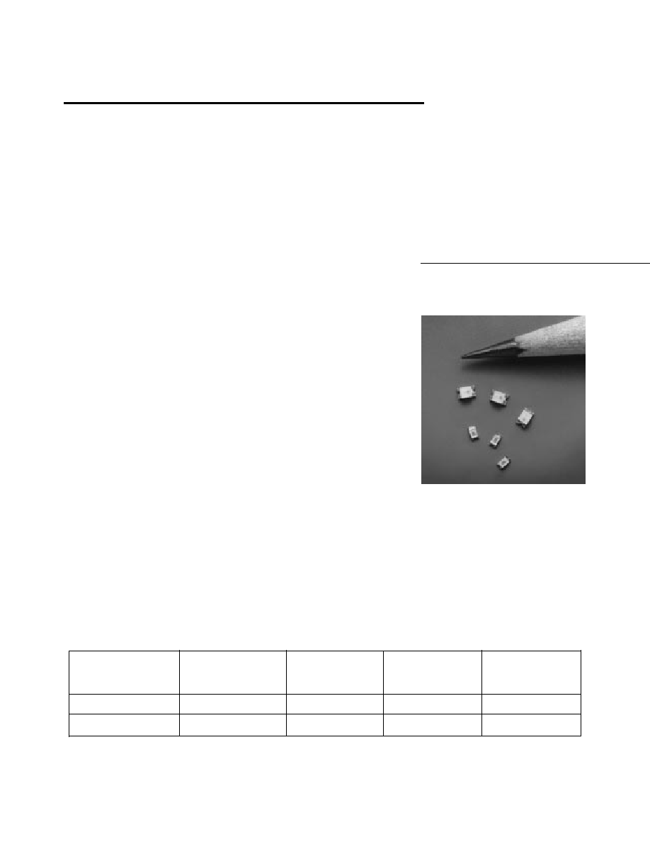
Surface Mount Flip Chip LEDs
Technical Data
Features
∑ Improved Reliability
Through Elimination of
Internal Wire Bond
∑ -40 to 85
∞
C Operating
Temperature Range
∑ Small Size
∑ Industry Standard Footprint
∑ Diffused Optics
∑ Compatible with IR
Solder Process
∑ Four Colors Available
∑ Available in 8 mm Tape on 7"
(178 mm) Diameter Reels
Applications
∑ Keypad Backlighting
∑ LCD Backlighting
∑ Symbol Backlighting
∑ Front Panel Indicator
Description
The HSMX-H670 and HSMX-H690
introduce a revolutionary concept
to the world of LEDs. The internal
flip chip construction eliminates
the wire bond between the chip
and printed circuit board.
Consequently as a result of the
robust construction, product
reliability is greatly improved.
The HSMX-H670 and HSMX-H690
are available in four colors. The
HSMX-H670 adheres to the
industry standard 2.0 x 1.25 mm
footprint and is intended for
designs where space is limited.
The small size, low 1.1 mm profile
and wide viewing angle make these
LEDs excellent for backlighting
applications and front panel
illumination. The HSMX-H690
adheres to the 1.6 x 0.8 mm
HSMX-H670 Series
HSMX-H690 Series
Notes:
1. Dimensions in mm.
2. Tolerance
±
0.1 mm unless otherwise noted.
industry standard footprint. The
low 0.6 mm profile make this
excellent for designs where
space is limited.
Both packages are compatible
with IR and convective reflow
soldering processes.
Absolute Maximum Ratings at T
A
= 25
∞
C
Parameter
HSMX-H670
HSMX-H690
Units
DC Forward Current
[1]
20
20
mA
Power Dissipation
50
50
mW
Reverse Voltage (I
R
= 100
µ
A)
5
5
V
Operating Temperature Range
-40 to +85
-40 to +85
∞
C
Storage Temperature Range
[2]
-40 to +85
-40 to +85
∞
C
Notes:
1. Derate linearly as shown in Figure 4 for temperatures above 25
∞
C.
2. Maximum temperature for tape and reel packaging is 60
∞
C.
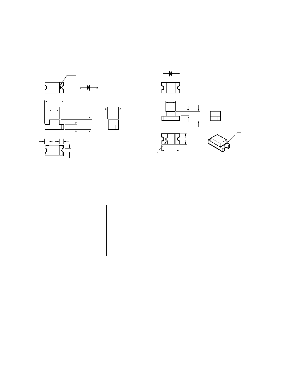
Package Dimensions
CATHODE MARK
2.00
(0.079)
1.10
(0.043)
0.50 (0.020)
0.40 (0.016)
1.25
(0.049)
1.27
(0.050)
POLARITY
0.48 (0.019)
0.40
(0.016)
HSMX-H670 Series
HSMX-H690 Series
NOTES:
1. DIMENSIONS ARE IN MILLIMETERS (INCHES).
2. TOLERANCE, UNLESS OTHERWISE SPECIFIED,
±
0.1 mm (
±
0.004 INCH).
3. THE LEADS ARE GOLD PLATED; PLATING THICKNESS IS: GOLD ≠ 0.05
MICRONS, NICKEL ≠ 3 MICRONS, COPPER ≠18 MICRONS.
,
0.60
0.30
1.00
POLARITY
0.80
1.60
BOTTOMSIDE CATHODE MARK
TOPSIDE
CATHODE
MARK
Optical Characteristics at T
A
= 25
∞
C
Luminous
Color,
Viewing
Luminous
Intensity
Peak
Dominant
Angle
Efficacy
I
V
(mcd)
Wavelength
Wavelength
2
1/2
v
Part
@ I
F
= 20 mA
[1]
peak
(nm)
d
[2]
(nm)
Degrees
[3]
(lm/W)
Number
Color
Min.
Typ.
Typ.
Typ.
Typ.
HSMS-H6X0
High
Efficiency
1.6
5.0
639
626
165
145
Red
HSMD-H6X0
Orange
1.6
4.0
606
604
165
380
HSMY-H6X0
Yellow
1.6
5.0
584
586
165
500
HSMG-H6X0
Green
4.0
9.0
566
571
165
595
Notes:
1. The luminous intensity I
V
is measured at the peak of the spatial radiation pattern which may not be aligned with the
mechanical axis of the lamp package.
2. The dominant wavelength
d
is derived from the CIE Chromaticity Diagram and represents the perceived color of the device.
3.
1/2
is the off-axis angle where the luminous intensity is 1/2 the peak intensity.
Electrical Characteristics at T
A
= 25
∞
C
Forward
Reverse
Capacitance
Voltage
Breakdown
C (pF),
Thermal
V
F
(Volts)
V
R
(Volts)
V
F
= 0,
Resistance
Part
@ I
F
= 20 mA
@ I
R
= 100
µ
A
f = 1 MHz
R
J-PIN
(
∞
C/W)
Number
Color
Typ.
Max.
Min.
Typ.
HSMS-H670
High Efficiency
2.0
2.6
5
6
250
HSMS-H690
Red
HSMD-H670
Orange
2.0
2.6
5
5
250
HSMD-H690
HSMY-H670
Yellow
2.1
2.6
5
5
250
HSMY-H690
HSMG-H670
Green
2.3
2.6
5
5
250
HSMG-H690
Green Color Bins
[1]
Bin ID
Minimum (nm)
Maximum (nm)
Notes
A
561.0
565.0
B
564.0
568.0
C
567.0
571.0
D
570.0
574.0
E
573.0
577.0
F
561.0
568.0
Bin A & Bin B
G
564.0
571.0
Bin B & Bin C
H
567.0
574.0
Bin C & Bin D
J
570.0
577.0
Bin D & Bin E
Luminous Intensity Bin Limits
[1]
Bin ID
Minimum (med)
Maximum (med)
A
0.10
0.20
B
0.16
0.32
C
0.25
0.50
D
0.40
0.80
E
0.63
1.25
F
1.00
2.00
G
1.60
3.20
H
2.50
5.00
J
4.00
8.00
K
6.30
12.50
L
10.00
20.00
M
16.00
32.00
N
25.00
50.00
P
40.00
80.00
Q
63.00
125.00
R
100.00
200.00
S
160.00
320.00
T
250.00
500.00
U
400.00
800.00
V
630.00
1250.00
W
1000.00
2000.00
X
1600.00
3200.00
Y
2500.00
5000.00
Note:
1. Bin categories are established for classification of products. Products may not be available in all bin categories.
Please contact your Hewlett-Packard representative for information on currently available bins.
Yellow Color Bins
[1]
Bin ID
Minimum (nm)
Maximum (nm)
Notes
A
581.5
585.0
B
584.0
587.5
C
586.5
590.0
D
589.0
592.5
E
581.5
587.5
Bin A & Bin B
F
584.0
590.0
Bin B & Bin C
G
586.5
592.5
Bin C & Bin D
H
591.5
595.0
J
594.0
597.5
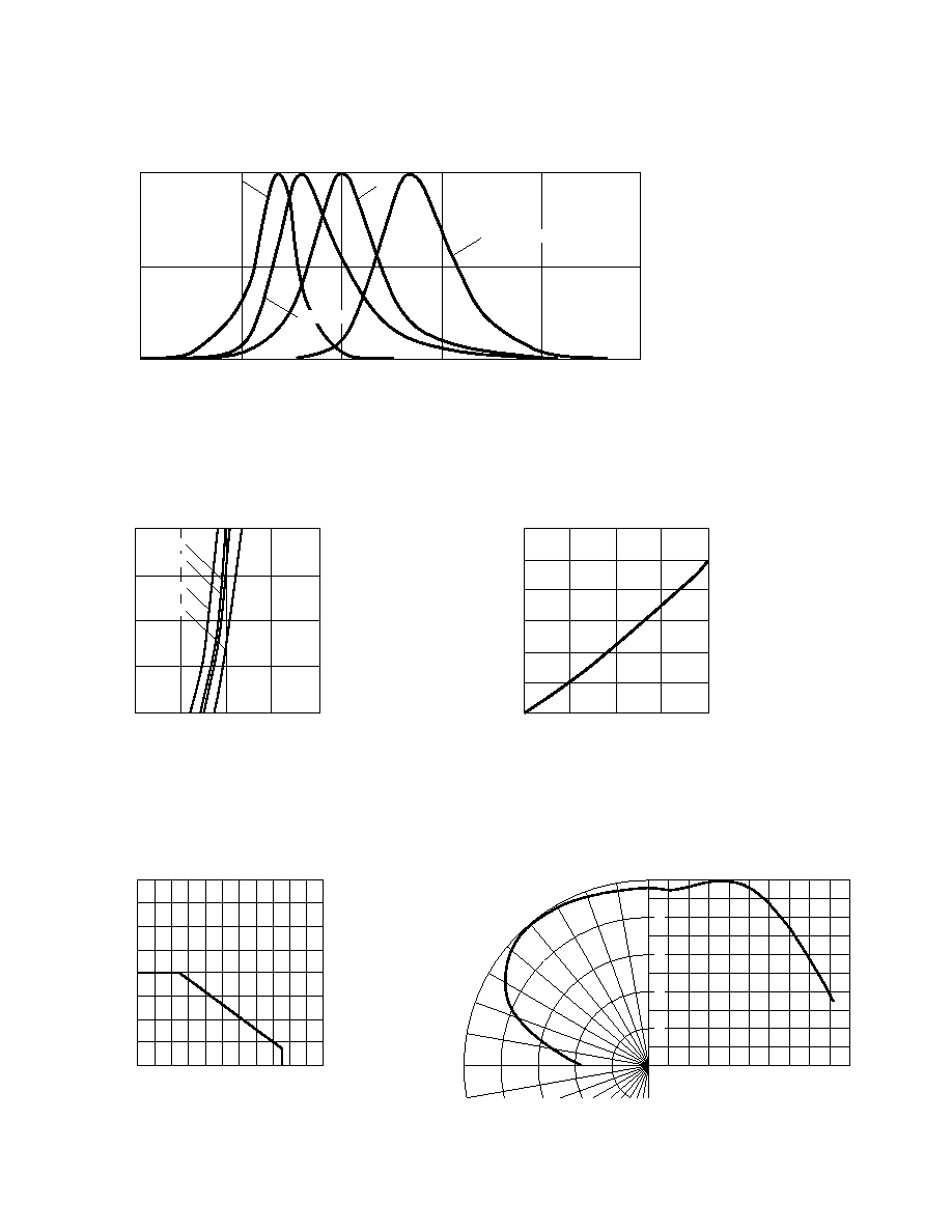
Figure 1. Relative Intensity vs. Wavelength.
WAVELENGTH ≠ nm
ORANGE
HIGH EFFICIENCY RED
GREEN
RELATIVE INTENSITY
1.0
0.5
0
500
550
600
650
700
750
YELLOW
Figure 4. Maximum DC Current vs. Ambient
Temperature.
Figure 5. Intensity vs. Angle.
0
20
40
60
80
100
TA ≠ AMBIENT TEMPERATURE ≠ ∞C
0
5
10
15
20
25
30
35
40
I F
≠ FORWARD CURRENT ≠ mA
10∞
100∞
40∞
70∞
20∞
60∞
80∞
30∞
50∞
90∞
NORMALIZED INTENSITY
ANGLE
0∞
10∞
20∞
30∞
40∞
50∞
60∞
70∞
80∞
90∞
1.0
.6
.8
.2
.4
20
10
0
1.0
1.5
2.0
2.5
3.0
VF ≠ FORWARD VOLTAGE ≠ V
I F
≠ FORWARD CURRENT ≠ mA
15
5
ORANGE
YELLOW
GREEN
HER
Figure 2. Forward Current vs. Forward Voltage.
Figure 3. Relative Luminous Intensity vs. DC Forward
Current.
0
5
10
15
20
IDC ≠ DC FORWARD CURRENT ≠ mA
0
0.2
0.4
0.6
0.8
1.0
1.2
RELATIVE LUMINOUS INTENSITY
(NORMALIZED AT 20 mA)
Document Outline
- List of Figures
- 1. Relative Intensity vs. Wavelength.
- 2. Forward Current vs. Forward Voltage.
- 3. Relative Luminous Intensity vs. DC Forward Current
- 4. Maximum DC Current vs. Ambient Temperature.
- 5. Intensity vs. Angle.
- 6. Recommended Reflow Soldering Profile.
- 7. Recommended Solder Patterns.
- 8. Reeling Orientation.
- 9. Reel Dimensions.
- 10. Tape Dimensions.
- 11. Tape Leader and Trailer Dimensions.
- Features
- Applications
- Description
- Device Selection Guide
- Package Dimensions
- HSMX-H670 Series
- HSMX-H690 Series
- Absolute Maximum Ratings at T A = 25∞C
- Optical Characteristics at T A = 25∞C
- Electrical Characteristics at T A = 25∞C
- Green Color Bins [1]
- Yellow Color Bins [1]
- Luminous Intensity Bin Limits [1]
- Convective IR Reflow Soldering