1-441
60 V/0.7 Ohm,
General Purpose, 1 Form A,
Solid State Relay
Technical Data
HSSR-8060
· Telecommunication
Switching Equipment
· Reed Relay Replacement
· 28 Vdc, 24 Vac, 48 Vdc Load
Driver
· Industrial Relay Coil Driver
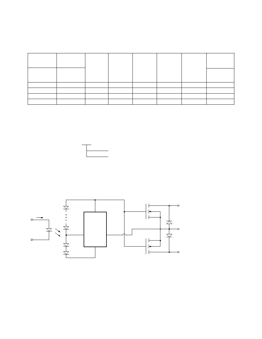
Description
The HSSR-8060 consists of a
high-voltage circuit, optically
coupled with a light emitting
diode (LED). This device is a
solid-state replacement for single-
pole, normally-open (1 Form A)
electromechanical relays used for
general purpose switching of
signals and low-power loads. The
relay turns on (contact closes)
with a minimum input current, I
F
,
of 5 mA through the input LED.
The relay turns off (contact
opens) with an input voltage, V
F
,
of 0.8 V or less. The detector
contains a high speed photosensi-
tive FET driver circuit and two
high voltage MOSFETs.
This relay's logic level input con-
trol and very low typical output
on-resistance of 0.4
makes it
suitable for both ac and dc loads.
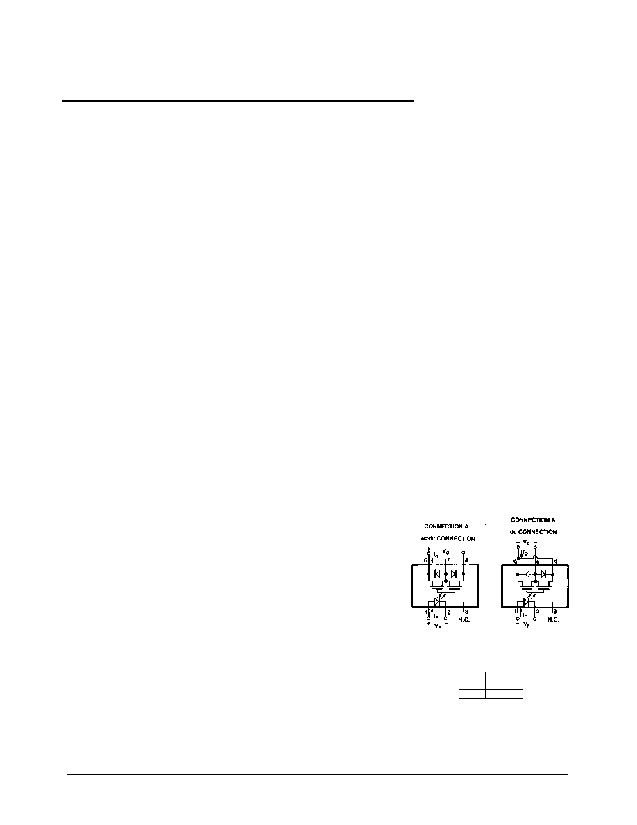
Connection A, as shown in the
schematic, allows the relay to
switch either ac or dc loads.
Connection B, with the polarity
and pin configuration as indicated
in the schematic, allows the relay
to switch dc loads only. The
advantage of Connection B is that
the on-resistance is significantly
reduced, and the output current
capability increases by a factor of
two.
The electrical and switching char-
acteristics of the HSSR-8060 are
specified from -40
°
C to +85
°
C.
Features
· Compact Solid-State
Bidirectional Switch
· Normally-Off Single-Pole
Relay Function (1 Form A)
· 60 V Output Withstand
Voltage in Both Polarities at
25
°
C
· 0.75/1.5 Amp Current
Ratings (See Schematic for
Connections A & B)
· Low Input Current; CMOS
Compatibility
· Very Low On-resistance:
0.4
Typical at 25
°
C
· ac/dc Signal and Power
Switching
· Input-to-Output Momentary
Withstand Insulation
Voltage: 2500 Vac, 1 Minute
· 16-kV ESD Immunity: MIL-
STD-883, Method 3015
· IEEE Surge Withstand
Capability (IEEE STD
472-1974)
· CSA Approved
· UL 508 Approved
Applications
· Programmable Logic
Controllers
CAUTION: It is advised that normal static precautions be taken in handling and assembly of this component to
prevent damage and/or degradation which may be induced by ESD.
Functional Diagram
TRUTH TABLE
(POSITIVE LOGIC)
LED
ON
OFF
OUTPUT
L
H
H
5965-3575E
1-444
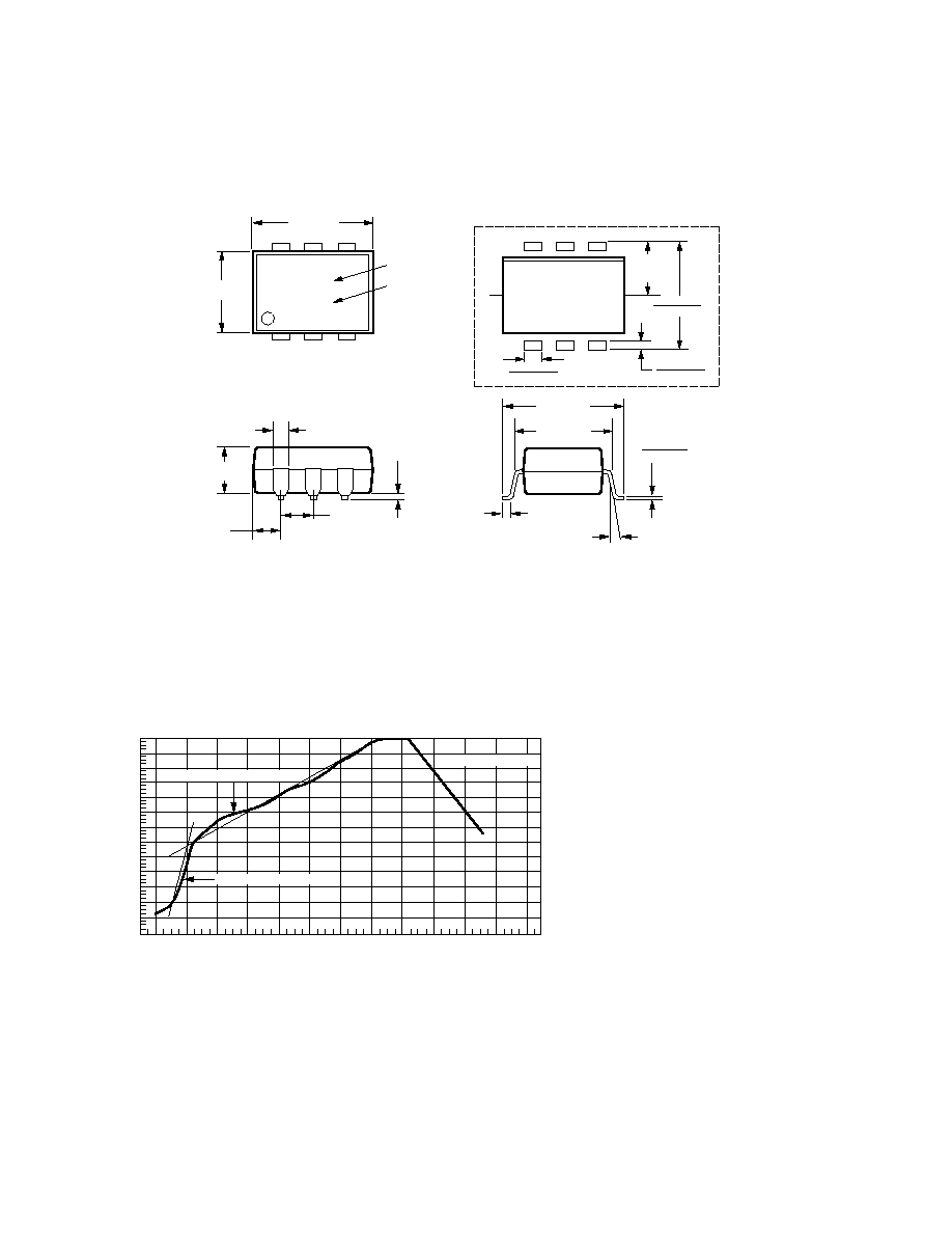
240
T = 115°C, 0.3°C/SEC
0
T = 100°C, 1.5°C/SEC
T = 145°C, 1°C/SEC
TIME MINUTES
TEMPERATURE °C
220
200
180
160
140
120
100
80
60
40
20
0
260
1
2
3
4
5
6
7
8
9
10
11
12
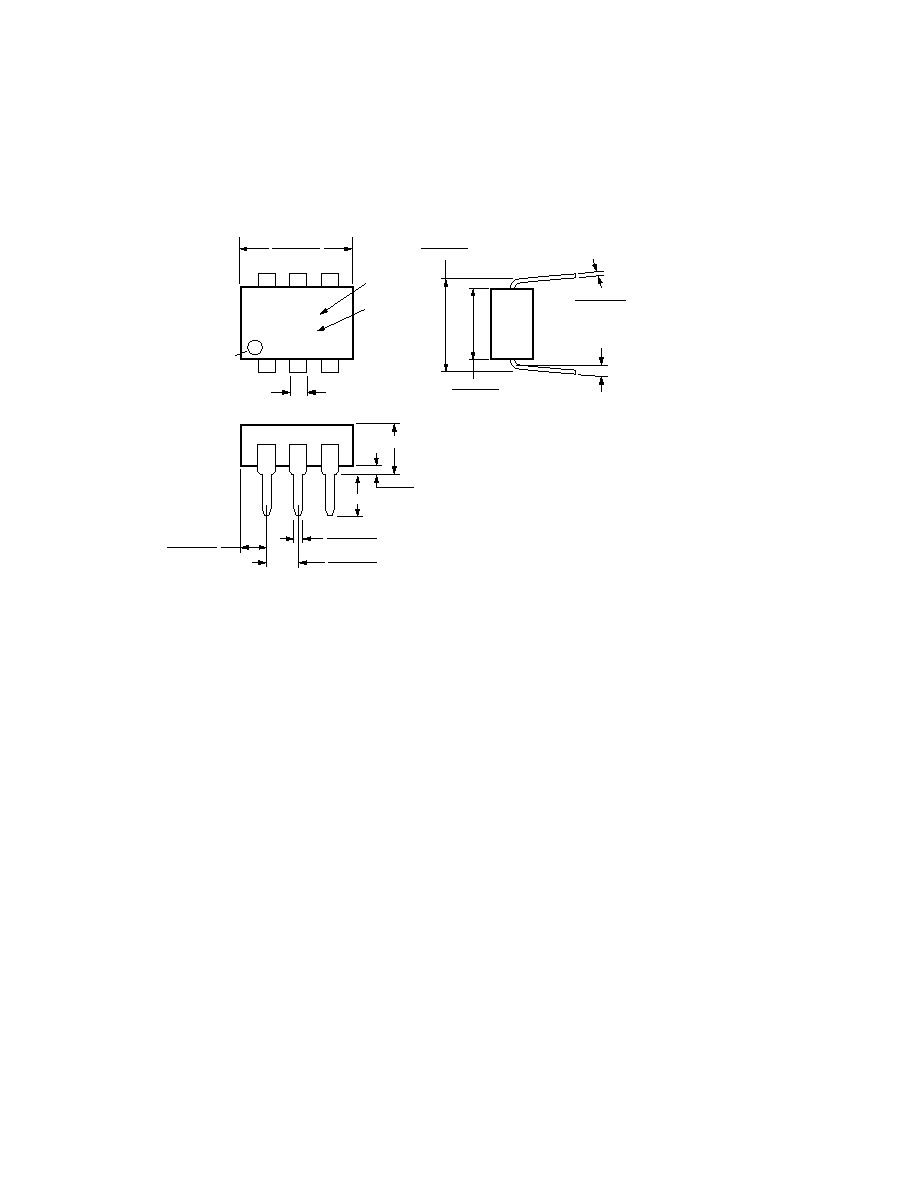
6-Pin Device Outline Drawing Option #300 (Gull Wing Surface Mount)
Thermal Profile (Option #300)
Regulatory Information
The HSSR-8060 has been
approved by the following
organizations:
UL
Recognized under UL 508,
Component Recognition Program,
Industrial Control Switches, File
E142465.
CSA
Approved under CAN/CSA-C22.2
No. 14-95, Industrial Control
Equipment, File LR 87683.
Figure 1. Maximum Solder Reflow Thermal Profile.
(Note: Use of non-chlorine activated fluxes is recommended.)
4.19
(0.165)
2.29
(0.090)
2.54
(0.100)
TYP.
0.635 ± 0.130
(0.025 ± 0.005)
9.65 ± 0.25
(0.380 ± 0.010)
7.62 ± 0.25
(0.300 ± 0.010)
0.635 ± 0.25
(0.025 ± 0.010)
12° NOM.
0.20 (0.008)
0.30 (0.013)
1.78
(0.070)
MAX.
9.65 ± 0.25
(0.380 ± 0.010)
6.35 ± 0.25
(0.250 ± 0.010)
DIMENSIONS IN mm (INCHES)
TOLERANCES: xx.xx = 0.01
xx.xxx = 0.001
(unless otherwise specified)
LEAD COPLANARITY
MAXIMUM: 0.102 (0.004)
[3] [5]
1.194 (0.047)
1.778 (0.070)
4.826
(0.190)
TYP.
9.398 (0.370)
9.906 (0.390)
MAX.
PAD LOCATION (FOR REFERENCE ONLY)
0.381 (0.015)
0.635 (0.025)
HP RXXXX
YYWW
TYPE NUMBER
DATE CODE

1-445
Insulation and Safety Related Specifications
Parameter
Symbol
Value
Units
Conditions
Min. External Air Gap
L(IO1)
7.0
mm
Measured from input terminals to output
(External Clearance)
terminals, shortest distance through air
Min. External Tracking Path
L(IO2)
8.5
mm
Measured from input terminals to output
(External Creepage)
terminals, shortest distance path along body
Min. Internal Plastic Gap
0.5
mm
Through insulation distance, conductor to
(Internal Clearance)
conductor, usually the direct distance
between the photoemitter and photodetector
inside the optocoupler cavity
Tracking Resistance
CTI
200
V
DIN IEC 112/VDE 0303 PART 1
(Comparative Tracking Index)
Isolation Group
IIIa
Material Group (DIN VDE 0110, 1/89, Table 1)
Option 300 surface mount classification is Class A in accordance with CECC 00802.
Absolute Maximum Ratings
Storage Temperature ................................................... -55
°
C to+125
°
C
Operating Temperature - T
A
.......................................... -40
°
C to +85
°
C
Case Temperature - T
C
.......................................................... +105
°
C
[1]
Average Input Current - I
F
............................................................ 20 mA
Repetitive Peak Input Current - I
F
............................................... 40 mA
(Pulse Width
1 ms; duty cycle
50%)
Transient Peak Input Current - I
F
............................................... 100 mA
(Pulse Width
200
µ
s; duty cycle
1%)
Reverse Input Voltage - V
R
................................................................ 3 V
Input Power Dissipation .............................................................. 40 mW
Output Voltage (T
A
= 25
°
C)
Connection A - V
O
......................................................... - 60 to +60 V
Connection B - V
O
............................................................. 0 to +60 V
Average Output Current - Figure 3 (T
A
= 25
°
C, T
C
70
°
C)
Connection A - I
O
..................................................................... 0.75 A
Connection B - I
O
..................................................................... 1.50 A
Single Shot Peak Output Current
(100 ms pulse width, T
A
= 25
°
C, I
F
= 10 mA)
Connection A - I
O
.................................................................... 3.75 A
Connection B - I
O
...................................................................... 7.0 A
Output Power Dissipation ..................................................... 750 mW
[2]
Lead Solder Temperature .... 260
°
C for 10 S (1.6 mm below seating plane)
Infrared and Vapor Phase Reflow Temperature
(Option #300) ......................................... See Fig. 1, Thermal Profile
Thermal Resistance
Typical Output MOSFET Junction
to Case
JC
= 55
°
C/W
Demonstrated ESD
Performance
Human Body Model: MIL-STD-
883 Method 3015.7 - 16 kV
Machine Model: EIAJ 1988.3.28
Version 2), Test Method 20,
Condition C 1200 V
Surge Withstand
Capability
IEEE STD 472-1974