Document Outline
- List of Figures
- 1. Typical Gain and Noise Figure vs. Frequency
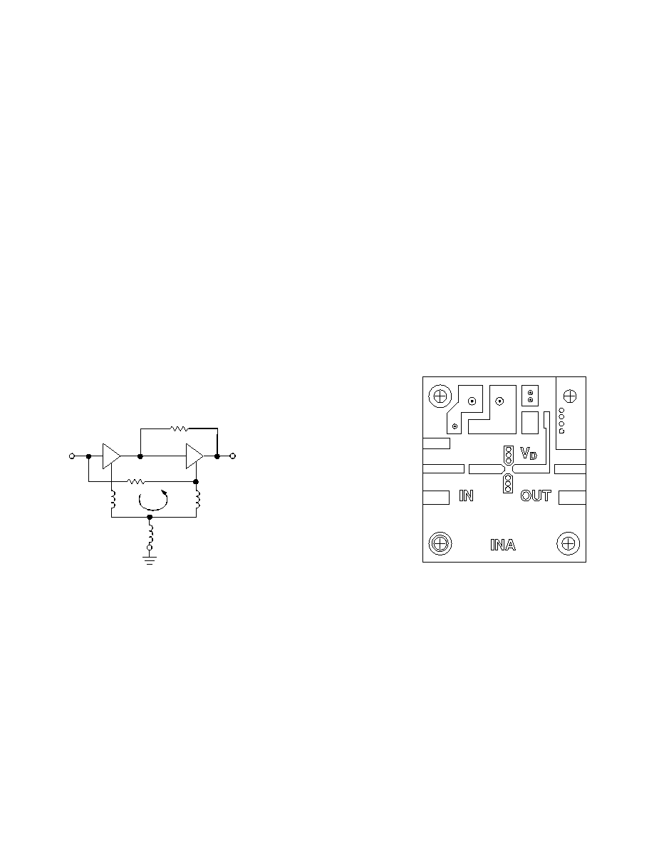
- 1. INA Potential Ground Loop
- 2. Device Current vs. Voltage
- 2. INA Circuit Board 2x Actual Size
- 3. Power Gain vs. Current
- 4. Output Power and 1 dB Gain Compression, NF and Power Gain vs. CaseTemperature
- 5. Output Power at 1 dB Gain Compression vs. Frequency
- 6. Noise Figure vs. Frequency
- 7. Input VSWR vs. Frequency Id = 35mA
- 8. Output VSWR vs. Frequency, Id = 35mA
- Features
- Description
- Typical Biasing Configuration
- Package 84
- Package 86
- INA-02184, -02186 Absolute Maximum Ratings
- INA-02184, -02186 Electrical Specifications [1] , TA = 25∞C
- INA-02184, -02186 Part Number Ordering Information
- INA-02184, -02186 Typical Performance
- Typical INA-02184 Scattering Parameters (Z O = 50 W, T A = 25∞C, I d = 35 mA)
- Typical INA-02186 Scattering Parameters (Z O = 50 W, T A = 25∞C, I d = 35 mA)
- Emitter Inductance and Performance
- Package 84 Dimensions
- Package 86 Dimensions

6-96
Low Noise, Cascadable
Silicon Bipolar MMIC Amplifier
Technical Data
Features
∑ Cascadable 50
Gain Block
∑ Low Noise Figure:
2.0 dB Typical at 0.5 GHz
∑ High Gain:
31 dB Typical at 0.5 GHz
26 dB Typical at 1.5 GHz
∑ 3 dB Bandwidth:
DC to 0.8 GHz
∑ Unconditionally Stable
(k>1)
∑ Low Cost Plastic Package
Package 84
Description
The INA-02184 and INA-02186 are
low-noise silicon bipolar Mono-
lithic Microwave Integrated
Typical Biasing Configuration
INA-02184
INA-02186
Package 86
C
block
C
block
R
bias
V
CC
V
d
= 5.5 V
RFC (Optional)
RF IN
RF OUT
4
1
2
3
Circuit (MMIC) feedback amplifi-
ers housed in low cost plastic
packages. They are designed for
narrow or wide bandwidth
commercial applications that
require high gain and low noise IF
or RF amplification.
The INA series of MMICs is
fabricated using HP's 10 GHz f
T
,
25 GHz f
MAX
, ISOSATTM-I silicon
bipolar process which uses nitride
self-alignment, submicrometer
lithography, trench isolation, ion
implantation, gold metallization
and polyimide intermetal dielec-
tric and scratch protection to
achieve excellent performance,
uniformity and reliability.
5965-9675E

6-97
INA-02184, -02186 Absolute Maximum Ratings
Parameter
Absolute Maximum
[1]
Device Current
50 mA
Power Dissipation
[2,3,4]
400 mW
RF Input Power
+13 dBm
Junction Temperature
+150
∞
C
Storage Temperature
≠65 to 150
∞
C
Thermal Resistance
[2]
:
jc
= 90
∞
C/W -- INA-02184
jc
= 100
∞
C/W -- INA-02186
Notes:
1. Permanent damage may occur if
any of these limits are exceeded.
2. T
CASE
= 25
∞
C.
3. Derate at 11.1 mW/
∞
C for T
C
>
144
∞
C for INA-02184.
4. Derate at 10 mW/
∞
C for T
C
> 110
∞
C
for INA-02186.
G
P
Power Gain (|S
21
|
2
)
f = 0.5 GHz
dB
29.0 31.0
29.0 31.0
G
P
Gain Flatness
f = 0.01 to 1.0 GHz
dB
±
2.0
±
2.0
f
3 dB
3 dB Bandwidth
[2]
GHz
0.8
0.8
ISO
Reverse Isolation (|S
12
|
2
)
f = 0.01 to 1.0 GHz
dB
39
39
Input VSWR (Max over Freq. Range)
f = 0.01 to 1.0 GHz
1.5
2.0
Output VSWR (Max over Freq. Range)
f = 0.01 to 1.0 GHz
1.7
1.7
NF
50
Noise Figure
f = 0.5 GHz
dB
2.0
2.0
P
1 dB
Output Power at 1 dB Gain Compression
f = 0.5 GHz
dBm
11
11
IP
3
Third Order Intercept Point
f = 0.5 GHz
dBm
23
23
t
D
Group Delay
f = 0.5 GHz
psec
330
350
V
d
Device Voltage
V
4.0
5.5
7.0
4.0
5.5
7.0
dV/dT
Device Voltage Temperature Coefficient
mV/
∞
C
+10
+10
Notes:
1. The recommended operating current range for this device is 30 to 40 mA. Typical performance as a function of current
is on the following page.
2. Referenced from 10 MHz Gain (G
P
).
INA-02184, -02186 Electrical Specifications
[1]
, T
A
= 25
∞
C
Symbol Parameters and Test Conditions: I
d
= 35 mA, Z
O
= 50
Units Min. Typ. Max. Min. Typ. Max.
VSWR
INA-02184, -02186 Part Number Ordering Information
Part Number
No. of Devices
Container
INA-02184-TR1
1000
7" Reel
INA-02184-BLK
100
Antistatic Bag
INA-02186-TR1
1000
7" Reel
INA-02186-BLK
100
Antistatic Bag
For more information, see "Tape and Reel Packaging for Semiconductor Devices".
INA-02184 INA-02186

6-98
INA-02184, -02186 Typical Performance, T
A
= 25
∞
C
(unless otherwise noted)
0
10
20
30
40
50
I
d
(mA)
G
p
(dB)
I
d
(mA)
0
4
6
2
8
V
d
(V)
Figure 2. Device Current vs. Voltage.
FREQUENCY (GHz)
FREQUENCY (GHz)
Figure 5. Output Power at 1 dB Gain
Compression vs. Frequency.
Figure 6. Noise Figure vs. Frequency.
NF (dB)
15
20
25
30
35
1.5
.01 .02
.05
0.1 0.2
0.5
1.0
2.0
2.0
2.5
3.0
3.5
G
p
(dB)
NF (dB)
FREQUENCY (GHz)
Figure 1. Typical Gain and Noise Figure
vs. Frequency, T
A
= 25
∞
C, I
d
= 35 mA.
T
C
= +85
∞
C
T
C
= +25
∞
C
T
C
= ≠25
∞
C
15
20
25
30
35
20
30
40
50
Figure 3. Power Gain vs. Current.
0.1 GHz
1.5 GHz
1.0 GHz
0.5 GHz
1.5
2.0
2.5
30
31
32
9
11
13
≠55
≠25
+25
+85
+125
.02
.05
0.1
0.5
0.2
2.0
1.0
.02
.05
0.1
0.5
0.2
2.0
1.0
NF (dB)
0
9
6
15
12
3
1.5
3.0
2.5
3.5
2.0
P
1 dB
(dBm)
P
1 dB
(dBm)
G
p
(dB)
TEMPERATURE (
∞
C)
Figure 4. Output Power and 1 dB Gain
Compression, NF and Power Gain vs.
CaseTemperature, f = 0.5 GHz, I
d
= 35 mA.
G
p
NF
I
d
= 40 mA
I
d
= 35 mA
I
d
= 30 mA
I
d
= 30 to 40 mA
Gain Flat to DC
P
1 dB
FREQUENCY (GHz)
Figure 7. Input VSWR vs. Frequency,
I
d
= 35 mA.
.02
.05
0.1
0.5
0.2
2.0
1.0
1.00:1
1.75:1
1.50:1
2.00:1
1.25:1
INA-02184
INA-02186
FREQUENCY (GHz)
Figure 8. Output VSWR vs. Frequency,
I
d
= 35 mA.
.02
.05
0.1
0.5
0.2
2.0
1.0
1.00:1
1.75:1
1.50:1
2.00:1
1.25:1
INA-02184
INA-02186

6-99
Typical INA-02184 Scattering Parameters (Z
O
= 50
, T
A
= 25
∞
C, I
d
= 35 mA)
Freq.
GHz
Mag
Ang
dB
Mag
Ang
dB
Mag
Ang
Mag
Ang
k
0.01
.09
≠176
31.9
39.33
≠1
≠40.0
.010
1
.25
≠1
1.40
0.05
.09
≠171
31.9
39.24
≠6
≠41.9
.008
≠12
.25
≠4
1.66
0.10
.10
≠163
31.8
39.07
≠13
≠40.9
.009
1
.25
≠8
1.52
0.20
.13
≠159
31.7
38.30
≠26
≠40.0
.010
15
.23
≠13
1.44
0.30
.15
≠161
31.4
37.30
≠39
≠38.4
.012
16
.22
≠17
1.29
0.40
.18
≠168
31.2
36.42
≠51
≠39.2
.011
32
.21
≠15
1.39
0.50
.19
≠175
31.0
35.40
≠63
≠40.0
.010
34
.21
≠16
1.52
0.60
.20
179
30.7
34.20
≠75
≠37.1
.014
35
.21
≠17
1.24
0.80
.19
166
29.9
31.21 ≠101
≠38.4
.012
38
.24
≠26
1.44
1.00
.17
159
28.4
26.36 ≠126
≠36.5
.015
53
.24
≠41
1.40
1.20
.15
159
26.8
21.89 ≠149
≠34.0
.020
56
.22
≠60
1.31
1.40
.15
163
24.8
17.36 ≠169
≠33.2
.022
62
.18
≠78
1.50
1.60
.16
168
22.6
13.59
175
≠31.4
.027
67
.14
≠93
1.50
1.80
.18
168
20.7
10.86
161
≠31.1
.028
61
.11
≠108
1.74
2.00
.19
165
18.8
8.71
149
≠30.2
.031
64
.08
≠125
1.92
2.50
.23
159
14.9
5.56
127
≠29.1
.035
56
.05
≠167
2.54
3.00
.27
150
11.5
3.76
106
≠27.1
.044
65
.04
156
2.89
3.50
.30
143
8.8
2.74
89
≠26.0
.050
57
.04
137
3.39
4.00
.33
133
6.6
2.14
73
≠25.0
.056
62
.05
137
3.78
S
11
S
21
S
12
S
22
Typical INA-02186 Scattering Parameters (Z
O
= 50
, T
A
= 25
∞
C, I
d
= 35 mA)
Freq.
GHz
Mag
Ang
dB
Mag
Ang
dB
Mag
Ang
Mag
Ang
k
0.01
.09
≠178
31.5
37.38
≠1
≠40.0
.010
1
.24
≠1
1.46
0.05
.09
≠172
31.5
37.55
≠6
≠37.7
.013
11
.24
≠5
1.22
0.10
.11
≠160
31.5
37.46
≠13
≠39.2
.011
8
.23
≠9
1.37
0.20
.14
≠153
31.4
37.04
≠25
≠40.9
.009
15
.22
≠17
1.60
0.30
.18
≠156
31.3
36.62
≠37
≠38.4
.012
1
.21
≠25
1.30
0.40
.22
≠161
31.2
36.20
≠49
≠37.7
.013
28
.19
≠30
1.25
0.50
.25
≠169
31.1
35.70
≠61
≠39.2
.011
42
.18
≠35
1.40
0.60
.28
≠177
30.9
34.94
≠74
≠38.4
.012
44
.16
≠39
1.33
0.80
.31
165
30.2
32.34 ≠101
≠36.5
.015
52
.15
≠47
1.20
1.00
.30
148
28.8
27.64 ≠129
≠34.4
.019
57
.12
≠59
1.15
1.20
.27
135
27.0
22.26 ≠153
≠32.4
.024
62
.09
≠70
1.15
1.40
.24
129
24.7
17.22 ≠173
≠31.1
.028
61
.07
≠80
1.23
1.60
.21
128
22.5
13.27
170
≠31.4
.027
62
.04
≠82
1.52
1.80
.20
129
20.4
10.42
156
≠29.1
.035
61
.02
≠83
1.50
2.00
.20
131
18.4
8.34
144
≠29.1
.035
63
.01
≠20
1.79
2.50
.23
133
14.5
5.29
123
≠27.1
.044
59
.02
30
2.15
3.00
.27
130
11.2
3.61
103
≠25.7
.052
63
.02
27
2.56
3.50
.31
124
8.3
2.60
86
≠24.4
.060
64
.02
34
2.97
4.00
.34
118
6.1
2.02
70
≠23.4
.068
58
.01
30
3.28
S
11
S
21
S
12
S
22

6-100
Emitter Inductance and
Performance
As a direct result of their circuit
topology, the performance of INA
MMICs is extremely sensitive to
groundpath ("emitter") induc-
tance. The two stage design
creates the possibility of a feed-
back loop being formed through
the ground returns of the stages. If
the path to ground provided by
the external circuit is "long" (high
in impedance) compared to the
path back through the ground
return of the other stage, then
instability can occur (see Fig. 1).
This phenomena can show up as a
"peaking" in the gain versus
frequency response (perhaps
creating a negative gain slope
amplifier), an increase in input
VSWR, or even as return gain (a
reflection coefficient greater than
unity) at the input of the MMIC.
The "bottomline" is that excellent
grounding is critical when
using INA MMICs. The use of
plated through holes or equivalent
minimal path ground returns at
the device is essential. An
appropriate layout is shown in
Figure 2. A corollary is that
designs should be done on the
thinnest practical substrate. The
parasitic inductance of a pair of
via holes passing through 0.032"
thick P.C. board is approximately
0.1 nH, while that of a pair of via
holes passing through 0.062" thick
board is close to 0.5 nH. HP does
not recommend using INA family
MMICs on boards thicker than
32 mils.
These stability effects are entirely
predictable. A circuit simulation
using the data sheet S-parameters
and including a description of the
ground return path (via model or
equivalent "emitter" inductance)
will give an accurate picture of the
performance that can be ex-
pected. Device characterizations
are made with the ground leads of
the MMIC directly contacting a
solid copper block (system
ground) at a distance of 2 to 4 mils
from the body of the package.
Thus the information in the data
sheet is a true description of the
performance capability of the
MMIC, and contains minimal
contributions from fixturing.
Figure 1. INA Potential
Ground Loop.
Figure 2. INA Circuit Board 2x
Actual Size.


