 | –≠–ª–µ–∫—Ç—Ä–æ–Ω–Ω—ã–π –∫–æ–º–ø–æ–Ω–µ–Ω—Ç: INA-03170 | –°–∫–∞—á–∞—Ç—å:  PDF PDF  ZIP ZIP |
Document Outline
- List of Figures
- 1. Typical Gain and Noise Figure vs. Frequency
- 2. Device Current vs. Voltage
- 3. Power Gain vs. Current
- 4. Output Power and 1 dB Gain Compression, NF and Power Gain vs. CaseTemperature
- 5. Output Power at 1 dB Gain Compression vs. Frequency
- 6. Noise Figure vs. Frequency
- Features
- Description
- Typical Biasing Configuration
- 70 mil Package
- INA-03170 Absolute Maximum Ratings
- INA-03170 Electrical Specifications , TA = 25∞C
- INA-03170 Typical Scattering Parameters
- INA-03170 Typical Performance
- 70 mil Package Dimensions

6-105
Low Noise, Cascadable
Silicon Bipolar MMIC Amplifier
Technical Data
Features
∑ Cascadable 50
Gain Block
∑ Low Noise Figure:
2.5 dB Typical at 1.5 GHz
∑ High Gain:
26.0 dB Typical at 1.5 GHz
∑ 3 dB Bandwidth:
DC to 2.8 GHz
∑ Unconditionally Stable
(k>1)
∑ Low Power Dissipation
∑ Hermetic Gold-Ceramic
Surface Mount Package
INA-03170
70 mil Package
Description
The INA-03170 is a low-noise
silicon bipolar Monolithic Micro-
wave Integrated Circuit (MMIC)
C
block
C
block
R
bias
(Required)
V
CC
> 7 V
V
d
= 4.5 V
RFC (Optional)
RF IN
RF OUT
4
1
2
3
Typical Biasing Configuration
feedback amplifier housed in a
hermetic, high reliability package.
It is designed for narrow or wide
bandwidth commercial, industrial
and military applications that
require high gain and low noise IF
or RF amplification with minimum
power consumption.
The INA series of MMICs is
fabricated using HP's 10 GHz f
T
,
25 GHz f
MAX
, ISOSATTM-I silicon
bipolar process which uses nitride
self-alignment, submicrometer
lithography, trench isolation, ion
implantation, gold metallization
and polyimide intermetal dielec-
tric and scratch protection to
achieve excellent performance,
uniformity and reliability.
5965-9677E
6-106
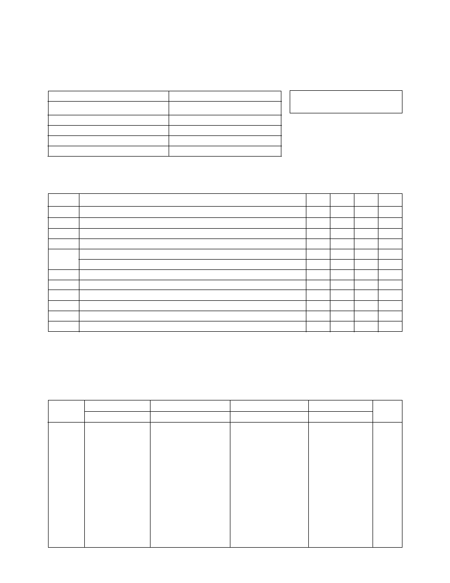
INA-03170 Absolute Maximum Ratings
Parameter
Absolute Maximum
[1]
Device Current
25 mA
Power Dissipation
[2,3]
200 mW
RF Input Power
+13 dBm
Junction Temperature
200
∞
C
Storage Temperature
≠65 to 200
∞
C
Thermal Resistance
[2,4]
:
jc
= 150
∞
C/W
Notes:
1. Permanent damage may occur if
any of these limits are exceeded.
2. T
CASE
= 25
∞
C.
3. Derate at 6.7 mW/
∞
C for T
C
> 170
∞
C.
4. See MEASUREMENTS section
"Thermal Resistance" for more
information.
G
P
Power Gain (|S
21
|
2
)
f = 1.5 GHz
dB
24.5
28.0
30.0
G
P
Gain Flatness
f = 0.01 to 2.0 GHz
dB
±
0.5
f
3 dB
3 dB Bandwidth
[2]
GHz
2.8
ISO
Reverse Isolation (|S
12
|
2
)
f = 0.01 to 2.0 GHz
dB
37
Input VSWR
f = 0.01 to 2.0 GHz
2.0
[3]
Output VSWR
f = 0.01 to 2.0 GHz
3.0
[3]
NF
50
Noise Figure
f = 1.5 GHz
dB
2.5
3.0
P
1 dB
Output Power at 1 dB Gain Compression
f = 1.5 GHz
dBm
1.0
IP
3
Third Order Intercept Point
f = 1.5 GHz
dBm
10
t
D
Group Delay
f = 1.5 GHz
psec
200
V
d
Device Voltage
f = 1.5 GHz
V
4.0
5.3
6.0
dV/dT
Device Voltage Temperature Coefficient
mV/
∞
C
+5
Notes:
1. The recommended operating current range for this device is 8 to 20 mA. Typical performance as a function of current is
on the following page.
2. Referenced from 10 MHz Gain (G
P
).
3. VSWR can be improved by bypassing the bias directly to ground.
INA-03170 Electrical Specifications
[1]
, T
A
= 25
∞
C
Symbol
Parameters and Test Conditions: I
d
= 12 mA, Z
O
= 50
Units
Min.
Typ.
Max.
VSWR
INA-03170 Typical Scattering Parameters (Z
O
= 50
, T
A
= 25
∞
C, I
d
= 12 mA)
Freq.
GHz
Mag
Ang
dB
Mag
Ang
dB
Mag
Ang
Mag
Ang
k
0.05
.35
178
26.6
21.48
≠4
≠35.9
.016
9
.56
≠1
1.24
0.10
.35
176
26.6
21.42
≠7
≠36.5
.015
6
.56
≠4
1.29
0.20
.34
172
26.6
21.37
≠14
≠36.5
.015
≠1
.56
≠7
1.30
0.40
.34
164
26.5
21.19
≠28
≠36.5
.015
≠5
.54
≠13
1.33
0.60
.33
158
26.4
20.91
≠41
≠38.4
.012
2
.53
≠18
1.58
0.80
.32
152
26.3
20.69
≠54
≠37.1
.014
5
.51
≠22
1.46
1.00
.32
147
26.2
20.48
≠67
≠36.5
.015
4
.50
≠27
1.41
1.20
.32
141
26.2
20.40
≠80
≠39.2
.011
13
.49
≠32
1.79
1.40
.31
133
26.3
20.73
≠93
≠37.7
.013
25
.48
≠38
1.57
1.60
.31
125
26.5
21.15 ≠106
≠37.1
.014
28
.47
≠45
1.47
1.80
.30
117
26.8
21.84 ≠121
≠35.4
.017
30
.46
≠52
1.28
2.00
.27
106
26.9
22.20 ≠138
≠37.1
.014
33
.42
≠62
1.48
2.50
.15
94
26.6
21.48 ≠177
≠35.4
.017
23
.31
≠79
1.44
3.00
.16
159
23.7
15.32
133
≠34.4
.019
42
.16
≠72
1.78
3.50
.28
150
19.8
9.81
99
≠35.4
.017
28
.19
≠60
2.71
S
11
S
21
S
12
S
22

6-107
INA-03170 Typical Performance, T
A
= 25
∞
C
(unless otherwise noted)
0
5
10
15
20
25
I
d
(mA)
I
d
(mA)
I
d
(mA)
0
4
6
2
10
8
V
d
(V)
Figure 2. Device Current vs. Voltage.
FREQUENCY (GHz)
FREQUENCY (GHz)
Figure 5. Output Power at 1 dB Gain
Compression vs. Frequency.
Figure 6. Noise Figure vs. Frequency.
NF (dB)
10
15
20
25
30
1.0
0.1
0.2
0.5
1.0
2.0
5.0
2.0
3.0
4.0
5.0
G
p
(dB)
NF (dB)
FREQUENCY (GHz)
Figure 1. Typical Gain and Noise Figure
vs. Frequency, T
A
= 25
∞
C, I
d
= 12 mA.
10
15
20
25
30
5
10
15
25
20
Figure 3. Power Gain vs. Current.
1.5
2.0
2.5
3.5
1.0
24
25
26
27
≠2
0
2
4
≠55
≠25
+25
+85
+125
0.1
0.2
0.5
2.0
1.0
5.0
0.1
0.2
0.5
2.0
1.0
5.0
NF (dB)
≠8
4
0
8
≠4
1.0
4.0
3.0
5.0
2.0
P
1 dB
(dBm)
P
1 dB
(dBm)
G
p
(dB)
TEMPERATURE (
∞
C)
Figure 4. Output Power and 1 dB Gain
Compression, NF and Power Gain vs.
CaseTemperature, f = 1.5 GHz, I
d
= 12 mA.
G
p
P
1 dB
NF
Gain Flat to DC
f = 0.1 ≠ 2 GHz
f = 3 GHz
f = 4 GHz
I
d
= 12 to 20 mA
I
d
= 8 mA
I
d
= 8 mA
I
d
= 12 mA
I
d
= 20 mA
T
C
= +125
∞
C
T
C
= +25
∞
C
T
C
= ≠55
∞
C
70 mil Package Dimensions
1
3
4
2
GROUND
GROUND
RF OUTPUT
AND BIAS
RF INPUT
.020
.508
.070
1.70
.495
±
.030
12.57
±
.76
Notes:
(unless otherwise specified)
1. Dimensions are in
2. Tolerances
in .xxx =
±
0.005
mm .xx =
±
0.13
mm
.040
1.02
.035
.89
.004
±
.002
.10
±
.05