Document Outline
- List of Figures
- 1. Typical Gain and Noise Figure vs. Frequency
- 2. Device Current vs. Voltage
- 3. Power Gain vs. Current
- 4. Output Power at 1 dB Gain Compression, NF and Power Gain vs. Case Temperature
- 5. Output Power at 1 dB Gain Compression vs. Frequency
- 6. Noise Figure vs. Frequency
- Features
- Description
- Typical Biasing Configuration
- 84 Plastic Package
- INA-03184 Absolute Maximum Ratings
- INA-03184 Electrical Specifications [1] , TA = 25∞C
- INA-03184 Part Number Ordering Information
- INA-03184 Typical Scattering Parameters
- INA-03184 Typical Performance, T A = 25∞C
- 84 Plastic Package Dimensions

6-108
Low Noise, Cascadable
Silicon Bipolar MMIC Amplifier
Technical Data
Features
∑ Cascadable 50
Gain Block
∑ Low Noise Figure:
2.6 dB Typical at 1.5 GHz
∑ High Gain:
25 dB Typical at 1.5 GHz
∑ 3 dB Bandwidth:
DC to 2.5 GHz
∑ Unconditionally Stable
(k>1)
∑ Low Power Dissipation:
10 mA Bias
∑ Low Cost Plastic Package
INA-03184
84 Plastic Package
Description
The INA-03184 is a low-noise
silicon bipolar Monolithic Micro-
wave Integrated Circuit (MMIC)
Typical Biasing Configuration
C
block
C
bypass
1
(Optional)
C
block
R
bias
V
CC
V
d
= 4.0 V
(Nominal)
RFC (Optional)
RF IN
RF OUT
4
1
2
3
Note:
1. VSWR can be improved by bypassing
a 100≠120
bias resistor directly to
ground. See AN-S012: Low Noise
Amplifiers.
feedback amplifier housed in a
low cost surface mount plastic
package. It is designed for narrow
or wide bandwidth commercial
and industrial applications that
require high gain and low noise IF
or RF amplification with minimum
power consumption.
The INA series of MMICs is
fabricated using HP's 10 GHz f
T
,
25 GHz f
MAX
, ISOSATTM-I silicon
bipolar process which uses nitride
self-alignment, submicrometer
lithography, trench isolation, ion
implantation, gold metallization
and polyimide intermetal dielec-
tric and scratch protection to
achieve excellent performance,
uniformity and reliability.
5965-9678E

6-109
INA-03184 Absolute Maximum Ratings
Parameter
Absolute Maximum
[1]
Device Current
25 mA
Power Dissipation
[2]
200 mW
RF Input Power
+13 dBm
Junction Temperature
150
∞
C
Storage Temperature
≠65 to 150
∞
C
Thermal Resistance:
jc
= 100
∞
C/W
Notes:
1. Permanent damage may occur if
any of these limits are exceeded.
2. Derate at 10 mW/
∞
C for T
C
> 130
∞
C.
INA-03184 Part Number Ordering Information
Part Number
No. of Devices
Container
INA-03184-TR1
1000
7" Reel
INA-03184-BLK
100
Antistatic Bag
For more information, see "Tape and Reel Packaging for Semiconductor Devices".
G
P
Power Gain (|S
21
|
2
)
f = 1.5 GHz
dB
23.0
25.0
G
P
Gain Flatness
f = 0.1 to 2.0 GHz
dB
±
0.8
f
3 dB
3 dB Bandwidth
[2]
GHz
2.5
ISO
Reverse Isolation (|S
12
|
2
)
f = 1.5 GHz
dB
35
Input VSWR
f = 0.01 to 2.0 GHz
2.0:1
Output VSWR
f = 0.01 to 2.0 GHz
3.0:1
[3]
NF
50
Noise Figure
f = 1.5 GHz
dB
2.6
P
1 dB
Output Power at 1 dB Gain Compression
f = 1.5 GHz
dBm
≠2.0
IP
3
Third Order Intercept Point
f = 1.5 GHz
dBm
7
t
D
Group Delay
f = 1.5 GHz
psec
210
V
d
Device Voltage
V
3.0
4.0
5.0
dV/dT
Device Voltage Temperature Coefficient
mV/
∞
C
+4
Notes:
1. The recommended operating current range for this device is 8 to 18 mA. Typical performance as a function of current is
on the following page.
2. Referenced from 10 MHz Gain (G
P
).
3. VSWR can be improved by bypassing a 100≠200
bias resistor directly to ground. See AN-S012: MagIC Low Noise
Amplifiers.
INA-03184 Electrical Specifications
[1]
, T
A
= 25
∞
C
Symbol
Parameters and Test Conditions: I
d
= 10 mA, Z
O
= 50
Units
Min.
Typ.
Max.
VSWR
6-110
INA-03184 Typical Scattering Parameters (Z
O
= 50
, T
A
= 25
∞
C, I
d
= 10 mA)
Freq.
GHz
Mag
Ang
dB
Mag
Ang
dB
Mag
Ang
Mag
Ang
k
0.05
.32
179
25.6
19.14
≠3
≠37.1
.014
3
.55
0
1.48
0.10
.32
176
25.6
19.05
≠7
≠37.1
.014
4
.57
≠3
1.45
0.20
.32
172
25.6
19.05
≠14
≠37.1
.014
6
.55
≠5
1.48
0.40
.32
165
2.5
18.78
≠29
≠37.1
.014
10
.53
≠11
1.53
0.60
.32
158
25.4
18.71
≠43
≠36.5
.015
11
.51
≠14
1.49
0.80
.32
151
25.4
18.53
≠57
≠36.5
.015
13
.51
≠17
1.50
1.00
.32
144
25.2
18.18
≠72
≠35.9
.016
21
.50
≠20
1.46
1.20
.30
135
25.2
18.27
≠86
≠35.9
.016
25
.50
≠23
1.46
1.40
.31
126
25.2
18.10 ≠102
≠35.4
.017
30
.49
≠29
1.42
1.60
.30
117
25.1
17.92 ≠117
≠34.9
.018
38
.48
≠34
1.38
1.80
.26
102
24.9
17.49 ≠135
≠34.4
.019
44
.45
≠41
1.39
2.00
.22
92
24.4
16.62 ≠153
≠34.0
.020
49
.40
≠50
1.44
2.50
.09
91
22.2
12.88
168
≠33.6
.021
57
.26
≠48
1.87
3.00
.14
160
18.9
8.79
134
≠32.8
.023
65
.22
≠33
2.40
3.50
.24
151
15.4
5.92
108
≠32.0
.025
69
.26
≠33
3.01
4.00
.29
139
12.4
4.18
87
≠30.8
.029
81
.28
≠43
3.52
Note:
1. S-parameters are de-embedded from 70 mil package measured data using the package model found in the DEVICE
MODELS section.
S
11
S
21
S
12
S
22
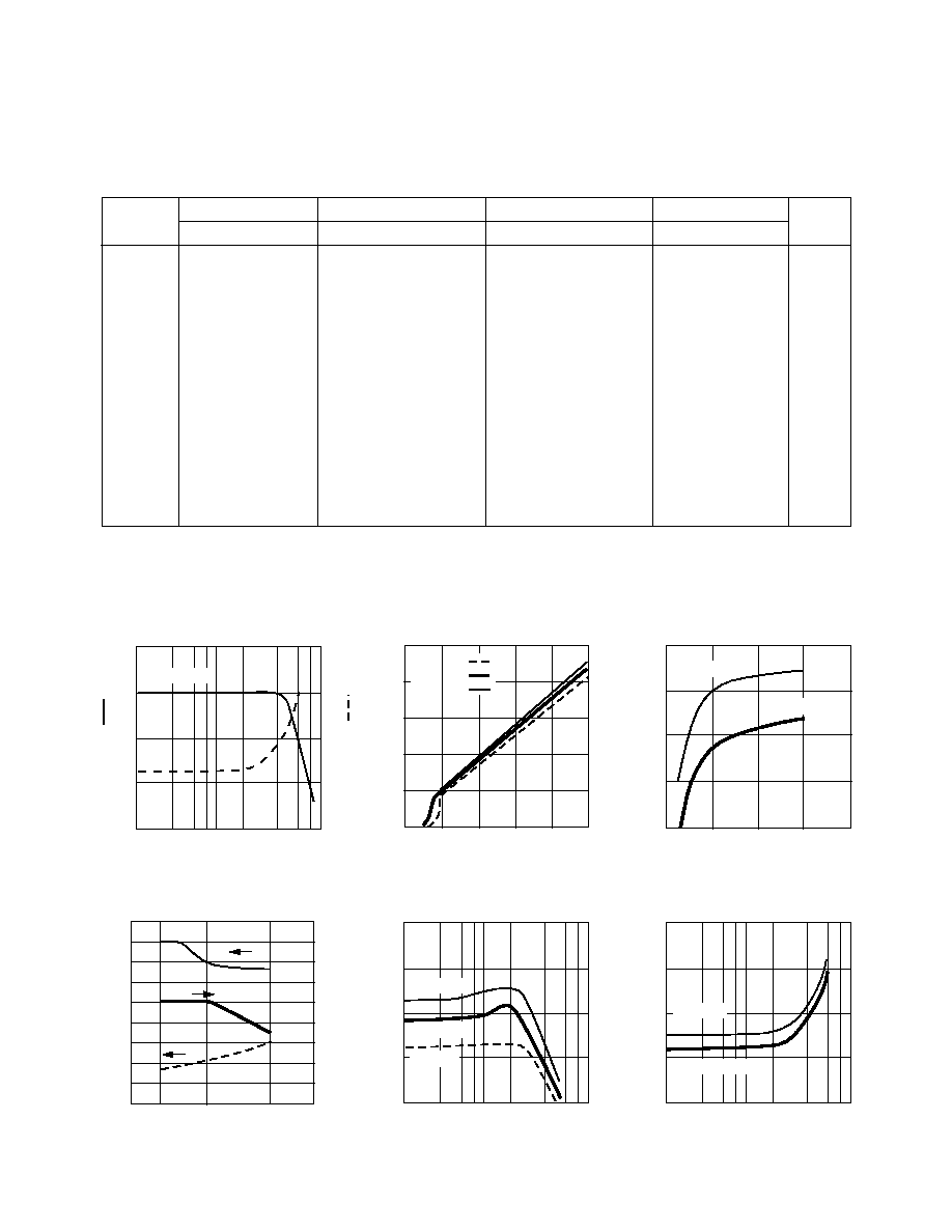
INA-03184 Typical Performance, T
A
= 25
∞
C
(unless otherwise noted)
0
5
10
15
20
25
I
d
(mA)
G
p
(dB)
I
d
(mA)
0
4
6
2
10
8
V
d
(V)
Figure 2. Device Current vs. Voltage.
FREQUENCY (GHz)
FREQUENCY (GHz)
Figure 5. Output Power at 1 dB Gain
Compression vs. Frequency.
Figure 6. Noise Figure vs. Frequency.
NF (dB)
10
15
20
25
30
1.0
0.1
0.2
0.5
1.0
2.0
5.0
2.0
3.0
4.0
5.0
G
p
(dB)
NF (dB)
FREQUENCY (GHz)
Figure 1. Typical Gain and Noise Figure
vs. Frequency, T
A
= 25
∞
C, I
d
= 10 mA.
T
C
= +85
∞
C
T
C
= +25
∞
C
T
C
= ≠25
∞
C
10
15
20
25
30
5
10
15
25
20
Figure 3. Power Gain vs. Current.
3.0
2.0
24
25
26
27
≠6
≠4
≠2
0
≠25
+25
+85
0.1
0.2
0.5
2.0
1.0
5.0
0.1
0.2
0.5
2.0
1.0
5.0
NF (dB)
≠8
4
0
8
≠4
1.0
4.0
3.0
5.0
2.0
P
1 dB
(dBm)
P
1 dB
(dBm)
G
p
(dB)
TEMPERATURE (
∞
C)
Figure 4. Output Power at 1 dB Gain
Compression, NF and Power Gain vs.
CaseTemperature, f = 1.5 GHz, I
d
= 10 mA.
G
p
P
1 dB
NF
Gain Flat to DC
f = 0.1 ≠ 2 GHz
f = 3 GHz
I
d
= 10 to 16 mA
I
d
= 8 mA
I
d
= 8 mA
I
d
= 10 mA
I
d
= 16 mA

6-111
84 Plastic Package Dimensions
1
4
3
2
0.51 (0.020)
0.51
(0.020)
DIMENSIONS ARE IN MILLIMETERS (INCHES)
0.20 ± 0.050
(0.008 ± 0.002)
2.15
(0.085)
1.52 ± 0.25
(0.060 ± 0.010)
5.46 ± 0.25
(0.215 ± 0.010)
5∞
GROUND
RF OUTPUT
AND DC BIAS
GROUND
RF INPUT
031