Document Outline
- List of Figures
- 1. Gain vs. Frequency
- 2. Input Return Loss vs. Frequency
- 3. Output Return Loss vs. Frequency
- 4. Gain at 900 MHz vs. Voltage and Temperature
- 5. Noise Figure at 900 MHz vs. Voltage and Temperature
- 6. Output P1dB at 900 MHz vs. Voltage and Temperature
- 7. Supply Current vs. Voltage and Temperature
- 8. Output P1 dB at 900MHz vs. Device Current for Vd = 3 V
- 9. INA-12063 Schematic.
- 10. Single-Resistor Bias Circuit
- 11. Shunt Stabilizing Resistor for LNA
- 12. PCB Pad Layout for INA-12063 Package
- 13. RF Layout
- 14. Stabilizing Resistor on Output
- 15. CAD File for Stability Analysis and Conjugate Match
- 16. 900 MHz LNA DC Schematic
- 17. Input Impedance Match
- 18. Input Circuit
- 19. Output Impedance Match
- 20. Output Circuit
- 21. PCB Layout of 900 MHz LNA
- 22. 900 MHz Amplifier Schematic
- 23. Completed 900 MHz LNA
- 24. Measured Gain of Example 900 MHz LNA
- 25. Measured Noise Figure of Example 900 MHz LNA
- 26. Measured Input and Output Return Loss of Example 900 MHz LNA
- 27. Measured Gain of Example 900 MHz LNA for Extended Frequency
- 28. Measured Input and Output Return Loss of Example 900 MHz
- 29. Surface Mount Assembly Profile
- 30. Normal Distribution
- 31. Phase Reference Planes
- 32. 900 MHz Test Circuit
- 33. 250 MHz Test Circuit
- Features
- Applications
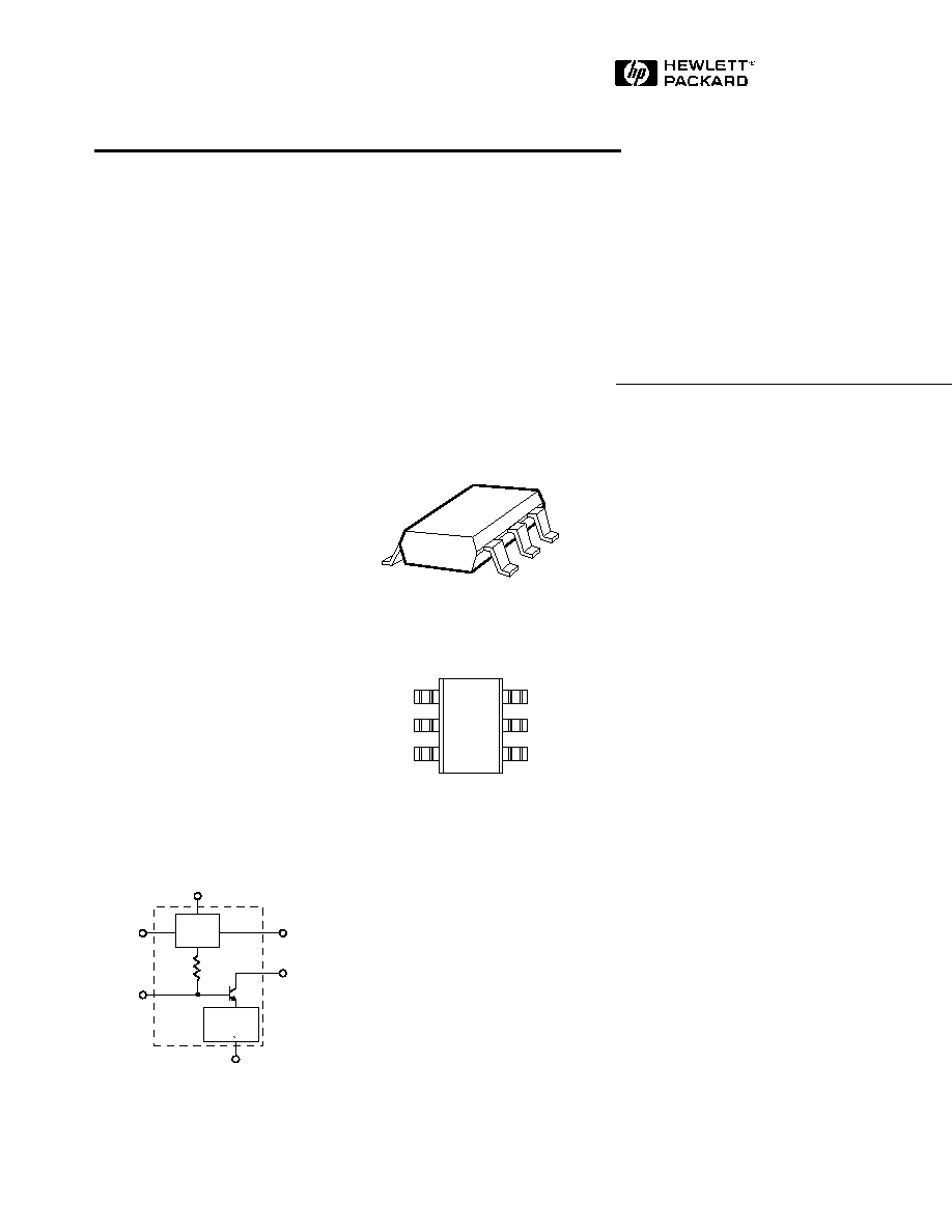
- Equivalent Circuit
- Surface Mount Package SOT-363
- Pin Connections and Package Marking
- Description
- INA-12063 Absolute Maximum Ratings
- Electrical Specifications
- INA-12063 Typical Performance
- INA-12063 Typical Scattering Parameters [1] , IC = 1.5 mA
- Typical Noise Parameters @ 900 MHz, IC = 1.5 mA
- INA-12063 Typical Scattering Parameters [1] , IC = 2.5 mA
- Typical Noise Parameters @ 900 MHz, IC = 2.5 mA
- INA-12063 Typical Scattering Parameters [1] , IC = 5 mA
- Typical Noise Parameters@ 900 MHz, IC= 5 mA
- INA-12063 Typical Scattering Parameters [1] , IC = 8 mA
- Typical Noise Parameters @ 900 MHz, IC = 8 mA
- INA-12063 Applications Information
- Description
- Setting the Bias Current
- PowerDown
- Amplifier Application Guidelines
- 900 MHz LNA Design Example
- Hints and Troubleshooting
- Phase Reference Planes
- Test Circuits
- Electrostatic Sensitivity
- Appendix A - Touchstone Circuit File
- Appendix B Ö Touchstone Output File
- INA-12063 Part Number Ordering Information
- Package Dimensions
6-116
Description
Hewlett-Packard's INA-12063 is a
Silicon monolithic self-biased
transistor amplifier that offers
excellent gain and noise figure for
applications to 1.5 GHz. Packaged
in an ultra-miniature SOT-363
package, it requires half the board
space of a SOT-143 package.
The INA-12063 is a unique RFIC
that combines the performance
flexibility of a discrete transistor
with the simplicity of using an
integrated circuit. Using a pat-
ented bias circuit, the perfor-
mance and operating current of
the INA-12063 can be adjusted
over the 1 to 10 mA range.
The INA-12063 is fabricated using
HP's 30 GHz f
MAX
ISOSATTM
Silicon bipolar process which
uses nitride self-alignment
submicrometer lithography,
trench isolation, ion implantation,
gold metalization, and polyimide
intermetal dielectric and scratch
protection to achieve superior
performance, uniformity, and
reliability.
1.5 GHz Low Noise Self-Biased
Transistor Amplifier
Technical Data
INA-12063
Features
∑ Integrated, Active Bias
Circuit
∑ Single Positive Supply
Voltage (1.5 ≠ 5V)
∑ Current Adjustable, 1 to
10mA
∑ 2 dB Noise Figure at
900 MHz
∑ 16 dB Gain at 900 MHz
25 dB Gain at 100 MHz
Applications
∑ Amplifier Applications for
Cellular, Cordless, Special
Mobile Radio, PCS, ISM,
and Wireless LAN
Applications
Surface Mount Package
SOT-363 (SC-70)
Pin Connections and
Package Marking
Equivalent Circuit
(Simplified)
Note:
Package marking provides orientation
and identification.
RF OUTPUT
and V
C
GND 1
12
I
bias
GND 2
RF INPUT
1
2
3
6
5
4 V
d
RF
INPUT
GND 1
RF
OUTPUT
and V
c
GND 2
V
d
I
bias
RF
FEEDBACK
NETWORK
ACTIVE
BIAS
CIRCUIT
5965-5365E

6-117
INA-12063 Absolute Maximum Ratings
Absolute
Symbol
Parameter
Units
Maximum
[1]
V
d
Supply Voltage, to Ground
V
7
V
c
Collector Voltage
V
7
I
c
Collector Current
mA
15
P
in
CW RF Input Power
dBm
13
T
j
Junction Temperature
∞
C
150
T
STG
Storage Temperature
∞
C
-65 to 150
Thermal Resistance
[2]
:
j-c
= 170
∞
C/W
Notes:
1. Operation of this device above any
one of these limits may cause
permanent damage.
2. T
C
= 25
∞
C (T
C
is defined to be the
temperature at the package pins
where contact is made to the
circuit board).
Electrical Specifications,
T
C
= 25
∞
C, V
d
= 3 V, unless noted
Symbol
Parameters and Test Conditions
Units Min.
Typ.
Max. Std.Dev.
[3]
G
P
Power Gain (|S
21
|
2
)
f = 900 MHz
[1]
dB
14.5
16
0.36
f = 250 MHz
[2]
19
NF
Noise Figure
f = 900 MHz
[1]
dB
2.0
2.6
0.2
f = 250 MHz
[2]
5.0
P
1dB
Output Power at 1 dB Gain Compression
f = 900 MHz
[1]
dBm
0
f = 250 MHz
[2]
-7
IP
3
Third Order Intercept Point
f = 900 MHz
[1]
dBm
15
f = 250 MHz
[2]
2
I
dd
Device Current
[4]
900 MHz LNA
[1]
mA
5
7
0.6
250 MHz IF Amp
[2]
1.5
Notes:
1. See Test Circuit in Figure 32.
2. See Test Circuit in Figure 33.
3. Standard deviation number is based on measurement of at least 500 parts from three non-consecutive wafer lots during
the initial characterization of this product, and is intended to be used as an estimate for distribution of the typical
specification.
4. I
dd
is the total current into Pins 1, 4, and 6 of the device, i.e. I
dd
= I
c
+ I
bias
+ I
d
.
6-118
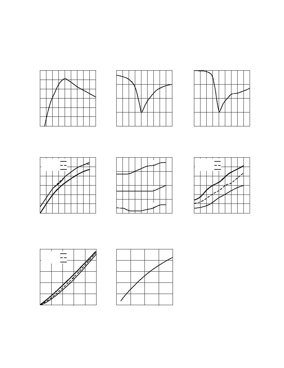
INA-12063 Typical Performance, 900 MHz LNA
(900 MHz Test Circuit, see Figure 32)
T
C
= 25
∞
C, Z
O
= 50
, V
d
= 3 V, I
C
= 5 mA, unless noted
Vd (V)
Figure 7. Supply Current vs. Voltage
and Temperature.
0
2
4
6
10
8
SUPPLY CURRENT (mA)
0.1
0.5 0.7 0.9 1.1
0.3
1.3
1.7
1.5
1.9
FREQUENCY (GHz)
Figure 1. Gain vs. Frequency.
-10
0
-5
10
5
15
20
GAIN (dB)
1
2
3
4
5
Vd (V)
Figure 4. Gain at 900 MHz vs. Voltage
and Temperature.
14.8
15.6
15.2
16.4
16.0
16.8
17.2
GAIN (dB)
0.1
0.5 0.7 0.9 1.1
0.3
1.3
1.7
1.5
1.9
FREQUENCY (GHz)
Figure 2. Input Return Loss vs.
Frequency.
-20
-10
-15
-5
0
RETURN LOSS (dB)
0.1
0.5 0.7 0.9 1.1
0.3
1.3
1.7
1.5
1.9
FREQUENCY (GHz)
Figure 3. Output Return Loss vs.
Frequency.
-20
-10
-15
-5
0
RETURN LOSS (dB)
T
A
= +85
∞
C
T
A
= +25
∞
C
T
A
= ≠40
∞
C
T
A
= +85
∞
C
T
A
= +25
∞
C
T
A
= ≠40
∞
C
1
2
3
4
5
Vd (V)
Figure 5. Noise Figure at 900 MHz vs.
Voltage and Temperature.
1.7
2.2
1.95
2.45
2.7
NOISE FIGURE (dB)
+85
∞
C
+25
∞
C
≠40
∞
C
1
2
3
4
5
Vd (V)
Figure 6. Output P
1dB
at 900 MHz vs.
Voltage and Temperature.
-2
0
-1
2
1
3
4
P
1dB
(dBm)
T
A
= +85
∞
C
T
A
= +25
∞
C
T
A
= ≠40
∞
C
1
0
2
3
4
5
DEVICE CURRENT (mA)
Figure 8. Output P
1 dB
at 900MHz vs.
Device Current for V
d
= 3 V.
-6
-3
0
3
9
6
P
1 dB
(dBm)
4
2
6
8
10

6-119
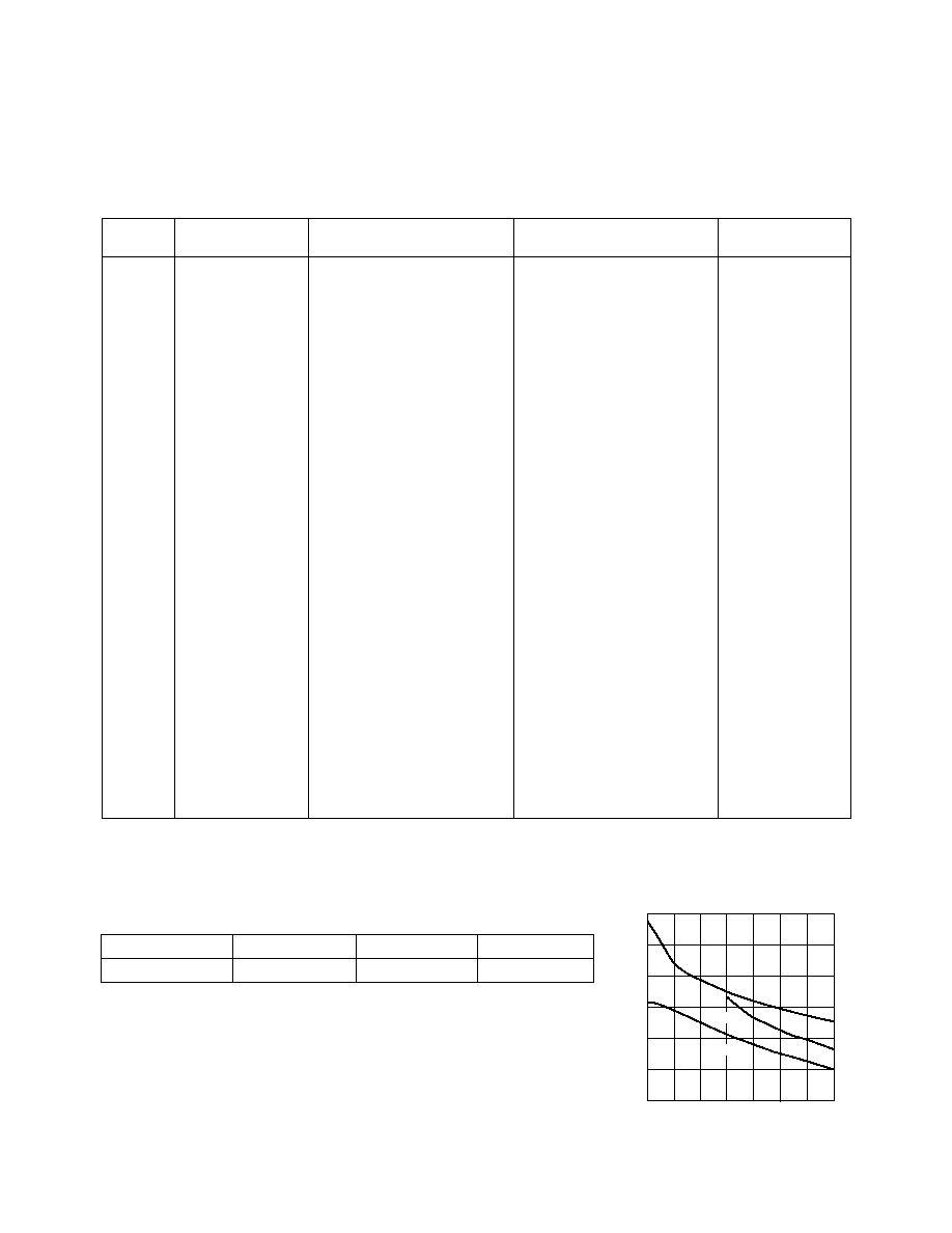
INA-12063 Typical Scattering Parameters
[1]
, I
C
= 1.5 mA
T
C
= 25
∞
C, Z
O
= 50
, V
d
= 3.0 V
Freq.
S
11
S
21
S
12
S
22
GHz
Mag.
Ang.
dB
Mag.
Ang.
dB
Mag.
Ang.
Mag.
Ang.
0.1
0.93
-8
12.6
4.26
172
-42.2
0.01
86
0.99
-3
0.2
0.92
-16
12.5
4.20
164
-36.2
0.02
79
0.99
-7
0.3
0.90
-24
12.3
4.11
157
-32.8
0.02
73
0.98
-10
0.4
0.89
-32
12.0
4.00
149
-30.5
0.03
69
0.96
-13
0.5
0.83
-38
11.7
3.83
141
-29.1
0.04
64
0.94
-16
0.6
0.79
-45
11.3
3.69
135
-27.9
0.04
60
0.93
-19
0.7
0.75
-52
10.9
3.49
128
-26.8
0.05
56
0.91
-21
0.8
0.72
-58
10.4
3.32
122
-26.1
0.05
53
0.89
-23
0.9
0.69
-64
10.1
3.18
116
-25.5
0.05
50
0.87
-26
1.0
0.65
-69
9.6
3.03
111
-24.9
0.06
47
0.86
-28
1.1
0.61
-74
9.2
2.89
106
-24.5
0.06
45
0.84
-30
1.2
0.59
-80
8.7
2.72
102
-24.2
0.06
43
0.83
-32
1.3
0.55
-84
8.4
2.64
97
-23.9
0.06
41
0.82
-34
1.4
0.52
-89
8.1
2.54
92
-23.6
0.07
40
0.81
-35
1.5
0.49
-94
7.7
2.43
88
-23.3
0.07
38
0.80
-37
1.6
0.47
-98
7.3
2.33
84
-23.2
0.07
36
0.79
-39
1.7
0.44
-103
7.0
2.23
80
-22.9
0.07
35
0.78
-40
1.8
0.42
-107
6.6
2.15
77
-22.9
0.07
35
0.77
-42
1.9
0.40
-112
6.4
2.08
73
-22.5
0.07
34
0.77
-44
2.0
0.38
-116
6.0
1.99
69
-22.3
0.08
33
0.76
-45
2.1
0.36
-120
5.7
1.93
66
-22.1
0.08
32
0.75
-47
2.2
0.34
-124
5.3
1.83
63
-22.0
0.08
29
0.74
-49
2.3
0.31
-129
5.2
1.82
59
-21.9
0.08
30
0.74
-51
2.4
0.31
-133
4.7
1.72
57
-22.0
0.08
29
0.73
-52
2.5
0.29
-137
4.6
1.70
54
-21.7
0.08
31
0.73
-54
2.6
0.28
-144
4.3
1.65
50
-21.4
0.08
30
0.73
-56
2.7
0.27
-149
4.1
1.60
47
-21.0
0.09
29
0.72
-58
2.8
0.25
-154
3.7
1.54
44
-20.7
0.09
27
0.71
-60
2.9
0.23
-156
3.5
1.50
41
-20.9
0.09
24
0.70
-61
3.0
0.24
-162
3.5
1.49
39
-21.0
0.09
28
0.71
-63
Note:
1. Reference plane per Figure 31 in Applications Information section.
0.1
0.9
1.7
2.5
FREQUENCY (GHz)
0
10
5
20
15
25
30
GAIN (dB)
MAG
MSG
|S
21
|
2
Typical Noise Parameters
@ 900 MHz, I
C
= 1.5 mA
Fmin (dB)
opt
Mag.
opt
Ang.
R
N
(
)
1.4
0.6
36
23
6-120
INA-12063 Typical Scattering Parameters
[1]
, I
C
= 2.5 mA
T
C
= 25
∞
C, Z
O
= 50
, V
d
= 3.0 V
Freq.
S
11
S
21
S
12
S
22
GHz
Mag.
Ang.
dB
Mag.
Ang.
dB
Mag.
Ang.
Mag.
Ang.
0.1
0.90
-10
16.0
6.33
171
-42.2
0.01
87
0.99
-4
0.2
0.88
-18
15.8
6.19
161
-36.2
0.02
79
0.98
-8
0.3
0.85
-27
15.5
5.98
153
-33.2
0.02
73
0.96
-11
0.4
0.82
-35
15.2
5.74
144
-31.1
0.03
68
0.94
-15
0.5
0.76
-42
14.6
5.37
135
-29.6
0.03
62
0.91
-18
0.6
0.71
-49
14.1
5.07
128
-28.4
0.04
59
0.90
-20
0.7
0.67
-56
13.5
4.73
122
-27.5
0.04
55
0.87
-23
0.8
0.62
-62
12.9
4.43
116
-26.6
0.05
53
0.85
-25
0.9
0.59
-67
12.4
4.18
110
-26.1
0.05
51
0.83
-27
1.0
0.54
-72
11.9
3.93
104
-25.6
0.05
49
0.82
-29
1.1
0.51
-76
11.4
3.71
100
-25.1
0.06
48
0.80
-30
1.2
0.49
-81
10.8
3.47
95
-24.8
0.06
46
0.79
-32
1.3
0.45
-84
10.4
3.31
91
-24.5
0.06
44
0.77
-34
1.4
0.42
-89
10.0
3.15
87
-24.1
0.06
44
0.76
-35
1.5
0.39
-93
9.5
2.98
83
-23.6
0.07
42
0.76
-37
1.6
0.37
-96
9.1
2.84
79
-23.5
0.07
41
0.74
-39
1.7
0.35
-100
8.7
2.72
76
-23.3
0.07
40
0.73
-40
1.8
0.33
-104
8.3
2.60
72
-23.0
0.07
41
0.73
-42
1.9
0.31
-108
8.0
2.51
69
-22.5
0.07
40
0.72
-43
2.0
0.29
-112
7.6
2.40
66
-22.2
0.08
40
0.72
-45
2.1
0.27
-115
7.3
2.31
62
-22.0
0.08
38
0.72
-47
2.2
0.25
-119
6.8
2.20
59
-21.8
0.08
36
0.71
-49
2.3
0.24
-122
6.6
2.15
56
-21.6
0.08
36
0.70
-50
2.4
0.23
-126
6.2
2.05
54
-21.7
0.08
36
0.69
-52
2.5
0.22
-131
6.1
2.01
51
-21.2
0.09
38
0.69
-53
2.6
0.20
-136
5.8
1.95
48
-20.7
0.09
36
0.69
-55
2.7
0.19
-142
5.5
1.89
45
-20.4
0.10
35
0.68
-57
2.8
0.18
-145
5.2
1.81
42
-20.0
0.10
32
0.68
-60
2.9
0.16
-146
4.9
1.75
39
-20.2
0.10
29
0.66
-60
3.0
0.17
-153
4.8
1.75
37
-20.1
0.10
32
0.68
-62
Note:
1. Reference plane per Figure 31 in Applications Information section.
0.1
0.9
1.7
2.5
FREQUENCY (GHz)
0
10
5
20
15
25
30
GAIN (dB)
|S
21
|
2
MSG
MAG
Typical Noise Parameters
@ 900 MHz, I
C
= 2.5 mA
Fmin (dB)
opt
Mag.
opt
Ang.
R
N
(
)
1.5
0.54
36
20