Agilent MGA-52543
Low Noise Amplifier
Data Sheet
Description
Agilent Technologies' MGA-52543
is an economical, easy-to-use GaAs
MMIC Low Noise Amplifier (LNA),
which is designed for use in LNA
and driver stages. While a capable
RF/microwave amplifier for any
low noise and high linearity 0.4 to
6 GHz application, the LNA focus
is Cellular/PCS base stations.
To attain NF
min
condition, some
simple external matching is re-
quired. The MGA-52543 features a
calculated NF
min
of 1.61 dB and 15
dB associated gain at 1.9 GHz from
a cascode stage, feedback FET
amplifier. The input and output are
partially matched to be near 50
.
For base station radio card unit
LNA application where better than
2:1 VSWR is required, a series
inductor on the input and another
series inductor on the output can
be added externally. The resulting
Noise Figure is typically 1.9 dB
with 14 dB Gain at 1.9 GHz. With a
single 5.0V supply, the LNA
Features
∑ Lead-free Option Available
∑ Operating frequency: 0.4 GHz ~
6.0 GHz
∑ Minimum noise figure: 1.61 dB at
1.9 GHz
∑ Associated gain : 15 dB at 1.9 GHz
∑ 1.9 GHz performance tuned for
VSWR < 2:1
Noise figure: 1.9 dB
Gain: 14 dB
P
1dB
: +17.5 dBm
Input IP3: +17.5 dBm
∑ Single supply 5.0 V operation
Applications
∑ Cellular/PCS base station radio
card LNA
∑ High dynamic range amplifier for
base stations, WLL, WLAN, and
other applications
Surface Mount Package
SOT-343/4-lead SC70
Pin Connections and
Package Marking
Simplified Schematic
typically draws 53 mA. This
alignment results in an Input
Intercept Point of 17.5 dBm.
The MGA-52543 is a GaAs MMIC,
fabricated using Agilent
Technologies' cost-effective,
reliable PHEMT (Pseudomorphic
High Electron Mobility Transistor)
process. It is housed in the SOT-343
(SC70 4-lead) package. This
package offers miniature size
(1.2 mm by 2.0 mm), thermal
dissipation, and RF characteristics.
42
GND
INPUT
OUTPUT
& V
d
GND
3
4
1
2
3.3 nH
2.2 nH
18 pF
V
d
5V
22 nH
MGA-52543
360 pF
Attention:
Observe precautions for
handling electrostatic
sensitive devices.
ESD Machine Model (Class A)
ESD Human Body Model (Class 1A)
Refer to Agilent Application Note A004R:
Electrostatic Discharge Damage and Control.
2
MGA-52543 Absolute Maximum Ratings
[1]
Symbol
Parameter
Units
Absolute Maximum
V
d
Maximum Input Voltage
V
±0.5
V
d
Supply Voltage
V
7.0
P
d
Power Dissipation
[2,3]
mW
425
P
in
CW RF Input Power
dBm
+20
T
j
Junction Temperature
∞C
160
T
STG
Storage Temperature
∞C
-65 to 150
Thermal Resistance:
[2]
jc
= 150
∞C/W
Notes:
1. Operation of this device in excess of any of
these limits may cause permanent damage.
2. T
case
= 25
∞C
Electrical Specifications
T
c
= +25
∞C, Z
o
= 50
, V
d
= 5V, unless noted
Symbol
Parameter and Test Condition
Frequency
Units
Min.
Typ.
Max.
[3]
I
d
test
Current drawn
N/A
mA
45
53
65
3.57
NF
[1]
Noise Figure
1.9 GHz
dB
1.9
2.3
0.15
0.9 GHz
1.8
Gain
[1]
Gain
1.9 GHz
dB
13
14.2
15.5
0.26
0.9 GHz
15
IIP3
[1]
Input Third Order Intercept Point
1.9 GHz
dBm
14
+17.5
2.28
0.9 GHz
+18
F
min
[2]
Minimum Noise Figure
1.9 GHz
dB
1.6
0.9 GHz
1.5
G
a
[2]
Associated Gain at F
min
1.9 GHz
dB
15.0
0.9 GHz
16.2
OIP3
[1]
Output Third Order Intercept Point
1.9 GHz
dBm
31.7
0.9 GHz
33.0
P
1dB
[1]
Output Power at 1 dB Gain Compression
1.9 GHz
dBm
+17.4
0.9 GHz
+18
RL
in
[1]
Input Return Loss
1.9 GHz
dB
11
0.9 GHz
15
RL
out
[1]
Output Return Loss
1.9 GHz
dB
20
0.9 GHz
22
ISOL
[1]
Isolation |s
12
|
2
1.9 GHz
dB
-25
0.9 GHz
-25
Notes:
1. Measurements obtained from a fixed narrow band tuning described in Figure 1. This circuit designed to optimize Noise Figure and IIP3 while
maintaining VSWR better than 2:1.
2. Minimum Noise Figure and Associated Gain at F
min
computed from S-parameter and Noise Parameter data measured in an automated NF system.
3. Standard deviation data are based on at least 400 part sample size and 11 wafer lots.
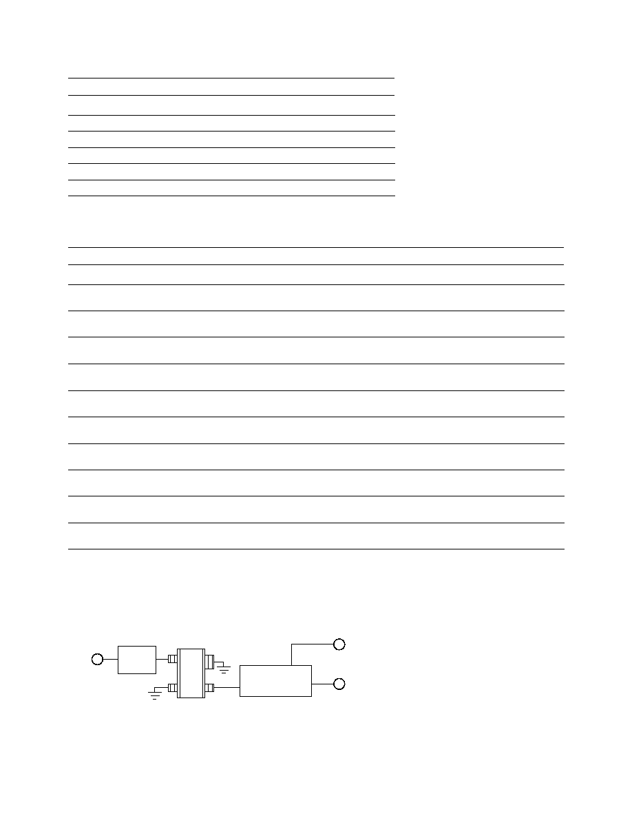
Figure 1. Block Diagram of Test Fixture.
See Figure 7 in the Applications section for an equivalent schematic of 1.9 GHz circuit; Figure 11 in the Applications section for 900 MHz circuit.
Input
Match
RF
Output
RF
Input
V
d
Output Match
and DC Bias
42
3
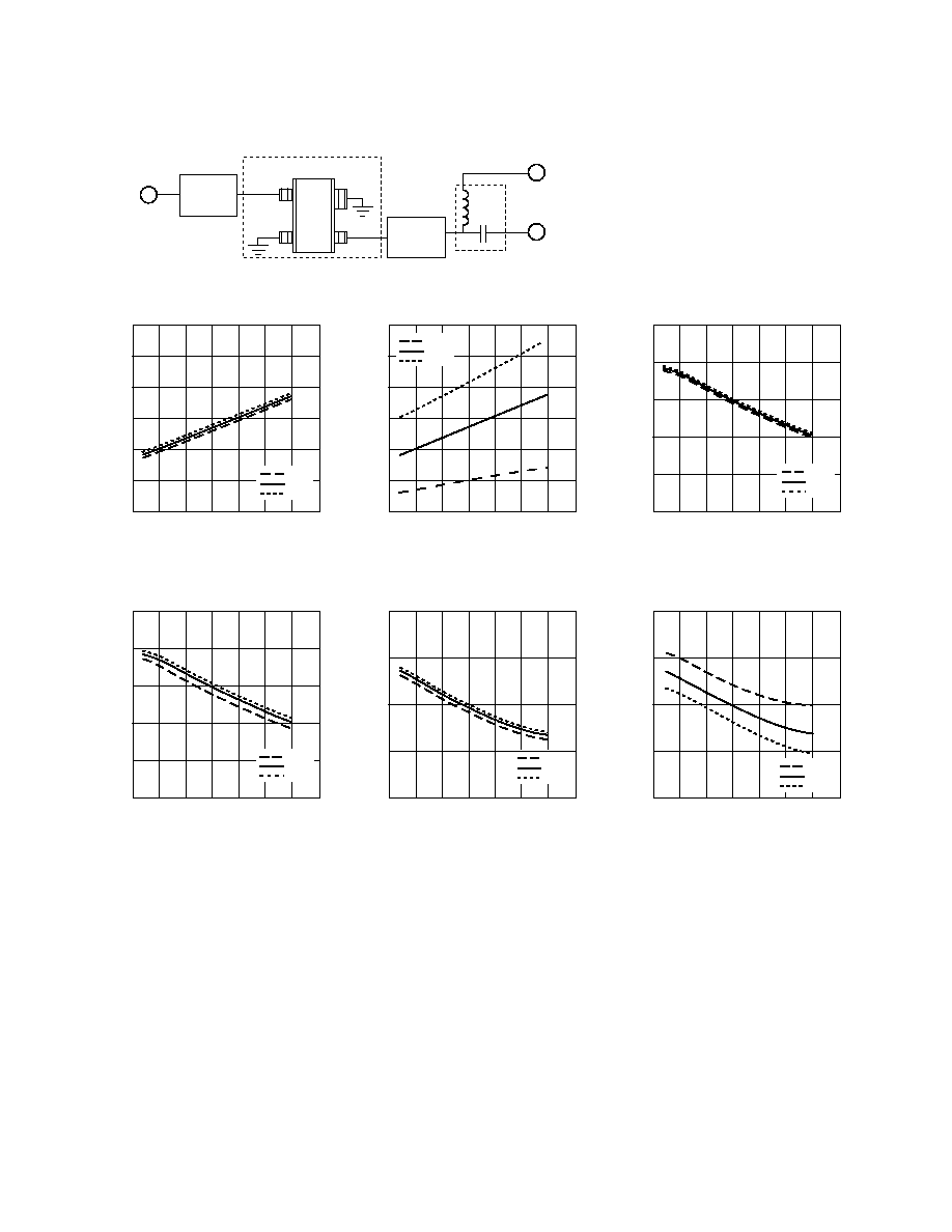
MGA-52543 Typical Performance
All data are measured at T
c
= 25
∞C, V
d
= 5V, and in the following test system unless stated otherwise.
Figure 2. Test Circuit for S, Noise, and Power Parameters over Frequency.
Tuner
Tuner
RF
Output
RF
Input
V
d
Bias
Tee
ICM Fixture
42
Notes:
1. Minimum Noise Figure and Associated Gain at F
min
computed from S-parameter and Noise Parameter data measured in an automated NF system.
2. Tuners on input and output were set for narrow band tuning designed to optimize NF and OIP3 while keeping VSWRs better than 2:1. See Figure 9
for corresponding return losses at each frequency band.
FREQUENCY (GHz)
Figure 3. Minimum Noise Figure vs.
Frequency and Voltage
[1]
.
F
min
(dB)
0
2.7
2.4
2.1
1.8
1.5
1.2
0.9
7
2
1
4
5
6
3
4.5 V
5.0 V
5.5 V
FREQUENCY (GHz)
Figure 4. Minimum Noise Figure vs.
Frequency and Temperature
[1]
.
F
min
(dB)
0
2.7
2.4
2.1
1.8
1.5
1.2
0.9
7
2
1
4
5
6
3
-40
∞C
+25
∞C
+85
∞C
FREQUENCY (GHz)
Figure 5. Associated Gain vs. Frequency
and Voltage
[1]
.
G
a
(dB)
0
20
17
14
11
8
5
7
2
1
4
5
6
3
4.5 V
5.0 V
5.5 V
FREQUENCY (GHz)
Figure 6. Associated Gain vs. Frequency
and Temperature
[1]
.
G
a
(dB)
0
20
17
14
11
8
5
7
2
1
4
5
6
3
-40
∞C
+25
∞C
+85
∞C
FREQUENCY (GHz)
Figure 7. Output Third Order Intercept Point
vs. Frequency and Voltage
[2]
.
OIP3 (dBm)
0
40
35
30
25
20
7
2
1
4
5
6
3
4.5 V
5.0 V
5.5 V
FREQUENCY (GHz)
Figure 8. Output Third Order Intercept Point
vs. Frequency and Temperature
[2]
.
OIP3 (dBm)
0
40
35
30
25
20
7
2
1
4
5
6
3
-40
∞C
+25
∞C
+85
∞C
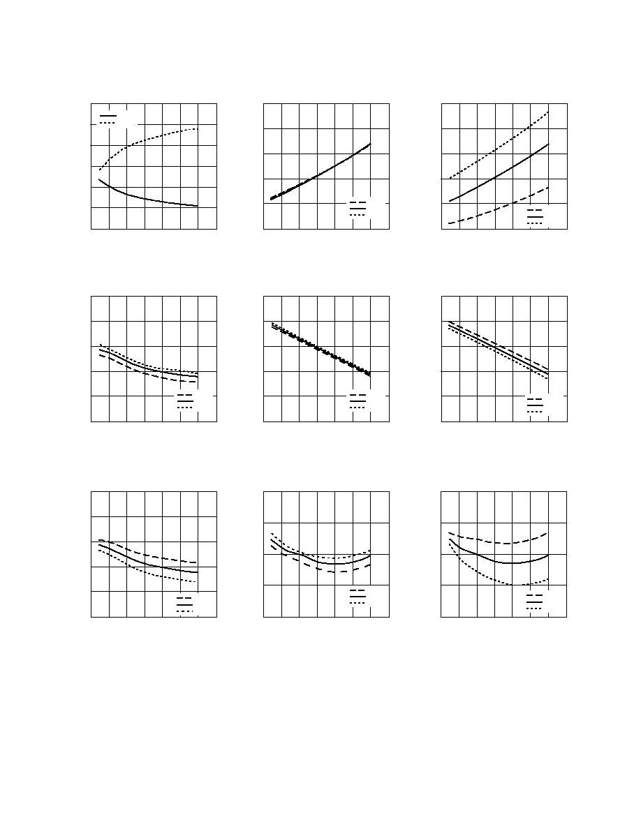
4
MGA-52543 Typical Performance,
continued
All data are measured at T
c
= 25
∞C, V
d
= 5V, and in the following test system unless stated otherwise.
Note:
All data reported from Figures 7 through 17 using test setup described in Figure 2. Tuners on input and output were set for narrow band tuning
designed to optimize NF and OIP3 while keeping VSWRs better than 2:1. See Figure 9 for corresponding return losses at each frequency band.
FREQUENCY (GHz)
Figure 9. Return Losses at each Narrow
Band Tuning.
RETURN LOSS (dB)
0
35
30
25
20
15
10
5
7
2
1
4
5
6
3
RL
in
RL
out
FREQUENCY (GHz)
Figure 10. Noise Figure vs. Frequency and
Voltage.
NF (dB)
0
3.2
2.8
2.4
2.0
1.6
1.2
7
2
1
4
5
6
3
4.5 V
5.0 V
5.5 V
FREQUENCY (GHz)
Figure 11. Noise Figure vs. Frequency and
Temperature.
NF (dB)
0
3.2
2.8
2.4
2.0
1.6
1.2
7
2
1
4
5
6
3
-40
∞C
+25
∞C
+85
∞C
FREQUENCY (GHz)
Figure 12. Output Power at 1 dB Compression
vs. Frequency and Voltage.
P
1d
B
(dBm)
0
25
22
19
16
13
10
7
2
1
4
5
6
3
4.5 V
5.0 V
5.5 V
FREQUENCY (GHz)
Figure 13. Gain vs. Frequency and
Temperature.
GAIN (dB)
0
20
17
14
11
8
5
7
2
1
4
5
6
3
4.5 V
5.0 V
5.5 V
FREQUENCY (GHz)
Figure 14. Gain vs. Frequency and
Temperature.
GAIN (dB)
0
20
17
14
11
8
5
7
2
1
4
5
6
3
-40
∞C
+25
∞C
+85
∞C
FREQUENCY (GHz)
Figure 15. Output Power at 1 dB Compression
vs. Frequency and Temperature.
P
1dB
(dBm)
0
25
22
19
16
13
10
7
2
1
4
5
6
3
-40
∞C
+25
∞C
+85
∞C
FREQUENCY (GHz)
Figure 16. Input Third Order Intercept Point
vs. Frequency and Voltage.
IIP3 (dBm)
0
21
19
17
15
13
7
2
1
4
5
6
3
4.5 V
5.0 V
5.5 V
FREQUENCY (GHz)
Figure 17. Input Third Order Intercept Point
vs. Frequency and Temperature.
IIP3 (dBm)
0
21
19
17
15
13
7
2
1
4
5
6
3
-40
∞C
+25
∞C
+85
∞C
5
Figure 18. Test Circuit for Figures 19 through 24 (Input and Output presented to 50
).
RF
Output
RF
Input
V
d
Bias
Tee
ICM Fixture
42
FREQUENCY (GHz)
Figure 19. Noise Figure vs. Frequency
(in 50
).
NF (dB)
0
3.0
2.6
2.2
1.8
1.4
1.0
7
2
1
4
5
6
3
FREQUENCY (GHz)
Figure 20. Gain vs. Frequency.
GAIN (dB)
0
20
17
14
11
8
5
7
2
1
4
5
6
3
FREQUENCY (GHz)
Figure 21. Input IP3, Output IP3 and P
1dB
vs.
Frequency.
IP3, P
1dB
(dBm)
0
32
28
24
20
16
12
7
2
1
4
5
6
3
OIP3
P
1dB
IIP3
FREQUENCY (GHz)
Figure 22. Isolation vs. Frequency.
ISOLATION (dB)
0
-15
-19
-23
-27
-31
-35
7
2
1
4
5
6
3
FREQUENCY (GHz)
Figure 23. Input and Output VSWR vs.
Frequency.
VSWR
0
5
4
3
2
1
7
2
1
4
5
6
3
In
Out
Vs (V)
Figure 24. Current vs. V
d
.
CURRENT (mA)
0
70
60
50
40
30
20
10
0
8
2
1
5
7
6
4
3
Id (-40∞C)
Id (+25∞C)
Id (+85∞C)
MGA-52543 Typical Performance,
continued