 | ÐлекÑÑоннÑй компоненÑ: MGA-725M4 | СкаÑаÑÑ:  PDF PDF  ZIP ZIP |
Äîêóìåíòàöèÿ è îïèñàíèÿ www.docs.chipfind.ru
Agilent MGA-725M4 Low Noise
Amplifier with Bypass Switch In
Miniature Leadless Package
Data Sheet
Description
Agilent Technologies's
MGA-725M4 is an economical,
easy-to-use GaAs MMIC Low
Noise Amplifier (LNA), which is
designed for an adaptive CDMA
receiver LNA and adaptive CDMA
transmit driver amplifier.
The MGA-725M4 features a typical
noise figure of 1.4 dB and 14.4 dB
associated gain from a single
stage, feedback FET amplifier.
The output is internally matched
to 50
. The input is optimally
internally matched for lowest
noise figure into 50
. The input
may be additionally externally
matched for low VSWR through
the addition of a single series
inductor. When set into the bypass
mode, both input and output are
internally matched to 50
.
Features
· Operating frequency:
0.1 GHz ~ 6.0 GHz
· Noise figure:
1.2 dB at 800 MHz
1.4 dB at 1900 MHz
· Gain:
17.5 dB at 800 MHz
15.7 dB at 1900 MHz
· Bypass switch on chip
Loss = typ 1.6 dB (I
d
< 5
µ
A)
IIP3 = +10 dBm
· Adjustable Input IP3:
+2 to +14.7 dBm
· Miniature package:
1.4 mm x 1.2 mm
2.7 V to 5.0 V operation
Applications
· CDMA (IS-95, J-STD-008) Receiver
LNA
· Transmit Driver Amp
· TDMA (IS-136) handsets
MiniPak 1.4 mm x 1.2 mm Package
Pin Connections and
Package Marking
The MGA-725M4 offers an
integrated solution of LNA with
adjustable IIP3. The IIP3 can be
fixed to a desired current level for
the receiver's linearity require-
ments. The LNA has a bypass
switch function, which sets the
current to zero and provides low
insertion loss. The bypass mode
also boosts dynamic range when
high level signal is being received.
For the CDMA driver amplifier
applications, the MGA-725M4
provides suitable gain and linear-
ity to meet the ACPR requirement
when the handset transmits the
highest power. When transmitting
lower power, the MGA-725M4 can
be bypassed, saving the drawing
current.
The MGA-725M4 is a GaAs MMIC,
processed on Agilent's cost
effective PHEMT (Pseudomorphic
High Electron Mobility Transistor).
It is housed in the MiniPak 1412
package. It is part of the Agilent
Technologies CDMAdvantage RF
chipset.
Simplified Schematic
GND
GND
Output
& V
d
Control
GainFET
Input
&
V
ref
A x
GROUND
INPUT
GROUND
OUTPUT
Ax

2
MGA-725M4 Absolute Maximum Ratings
[1]
Symbol
Parameter
Units
Absolute
Operation
Maximum
Maximum
V
d
Maximum Input to Output Voltage
V
5.5
4.2
V
gs
Maximum Input to Ground DC Voltage
V
+.3
+.1
-5.5
-4.2
I
d
Supply Current
mA
70
60
P
d
Power Dissipation
[1,2]
mW
300
250
P
in
CW RF Input Power
dBm
+20
+13
T
j
Junction Temperature
°
C
170
150
T
STG
Storage Temperature
°
C
-65 to +150
-40 to +85
Thermal Resistance:
[2]
jc
= 180
°
C/W
Notes:
1. Operation of this device in excess of any of
these limits may cause permanent damage.
2. T
case
= 25
°
C.
Electrical Specifications, T
c
= +25
°
C, Z
o
= 50
, I
d
= 20 mA, V
d
= 3V, unless noted.
Symbol
Parameter and Test Condition
Units
Min.
Typ.
Max.
V
gs
test
[1]
f = 2.0 GHz V
d
= 3.0 V (V
ds
= 2.5V)
I
d
= 20 mA
V
-0.65
-0.51
-0.37
0.035
NF test
[1]
f = 2.0 GHz V
d
= 3.0V (= V
ds
- V
gs
)
I
d
= 20 mA
dB
1.4
1.8
0.06
Ga test
[1]
f = 2.0 GHz V
d
= 3.0V (= V
ds
- V
gs
)
I
d
= 20 mA
dB
13.5
14.4
15.5
0.42
IIP3 test
[1]
f = 2.04 GHz V
d
= 3.0V (= V
ds
- V
gs
)
I
d
= 20 mA
dB
8.5
9.9
0.35
IL test
[1,4]
f = 2.0 GHz V
d
= 3.0 V (V
ds
= 0V, V
gs
= -3V)
I
d
= 0.0 mA
dB
1.6
3.5
0.07
Ig test
[1,4]
f = 2.0 GHz V
d
= 3.0 V (V
ds
= 0V, V
gs
= -3V)
I
d
= 0.0 mA
µ
A
2.0
2.0
Nfo
[2]
Minimum Noise Figure
f = 1.0 GHz
dB
1.2
As measured in Figure 2 Test Circuit
f = 1.5 GHz
1.2
(Computed from s-parameter and noise
f = 2.0 GHz
1.3
parameter performance as measured in a
f = 2.5 GHz
1.3
50
impedance fixture)
f = 4.0 GHz
1.4
f = 6.0 GHz
1.6
Gain
[2]
Associated Gain at Nfo
f = 1.0 GHz
dB
17.6
As measured in Figure 2 Test Circuit
f = 1.5 GHz
16.6
(Computed from s-parameter and noise
f = 2.0 GHz
15.7
parameter performance as measured in a
f = 2.5 GHz
14.8
50
impedance fixture)
f = 4.0 GHz
12.8
f = 6.0 GHz
10.6
P1dB
[1]
Output Power at 1 dB Gain Compression
I
d
= 0 mA
dBm
15.2
As measured in Figure 1 Test Circuit
I
d
= 5 mA
3.4
Frequency = 2.04 GHz
I
d
= 10 mA
9.14
I
d
= 20 mA
13.13
0.53
I
d
= 40 mA
15.25
I
d
= 60 mA
16.16
IIP3
[1]
Input Third Order Intercept Point
I
d
= 0 mA
dBm
35
As measured in Figure 1 Test Circuit
I
d
= 5 mA
3.1
Frequency = 2.04 GHz
I
d
= 10 mA
6.6
I
d
= 20 mA
9.9
0.35
I
d
= 40 mA
13.0
I
d
= 60 mA
14.7
RLin
[1]
Input Return Loss as measured in Fig. 1
f = 2.0 GHz
dB
-8.2
0.41
RLout
[1]
Output Return Loss as measured in Fig. 1
f = 2.0 GHz
dB
-15
1.3
ISOL
[1]
Isolation |S
12
|
2
As measured in Fig. 2
f = 2.0 GHz
dB
-23.4
0.4
Notes:
1. Standard deviation and typical data as measured in the test circuit of Figure 1. Data based on 500 part sample size from 3 wafer lots.
2. Typical data computed from S-parameter and noise parameter data measured in a 50
system.
3. V
d
= total device voltage = V
dg
4. Bypass mode voltages shown are used in production test. For source resistor biasing, Bypass mode is set by opening the source resistor.
3
MGA-725M4 Typical Performance
Frequency = 2.0 GHz, T
c
= 25
°
C, Z
o
= 50
, V
d
= 3V, I
d
= 20 mA unless stated otherwise. All data as measured in Figure 2
test system (input and output presented to 50
).
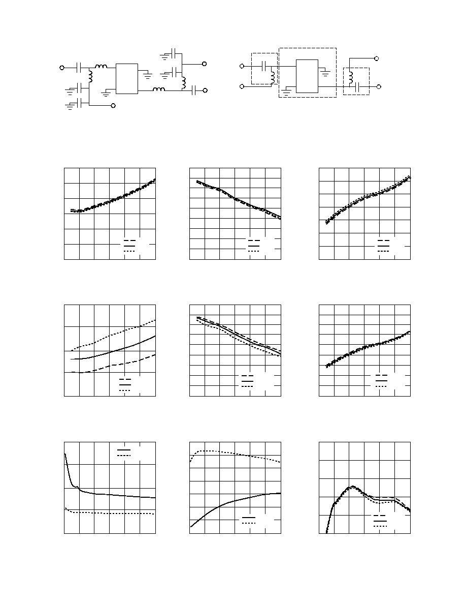
Figure 1. MGA-725M4 Production Test Circuit.
Figure 2. MGA-725M4 50
Test Circuit for S, Noise, and Power
Parameters.
RF
Input
V
gs
47 pF
1000 pF
1.2 nH
27 nH
27 nH
2.7 nH
1000 pF
100 pF
V
ds
RF
Output
Ax
100 pF
47 pF
RF
Input Bias Tee
V
d
RF
Output
Ax
V
gs
Bias
Tee
ICM Fixture
0
0.5
1.0
3.0
2.5
2.0
1.5
0
1
2
3
4
6
5
NF
(dB)
FREQUENCY (GHz)
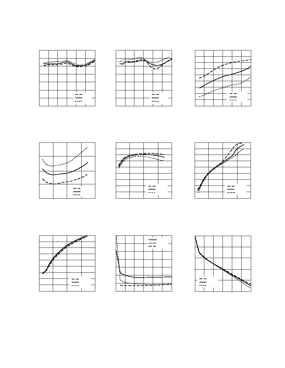
Figure 3. Noise Figure vs. Frequency and
Voltage.
2.7 V
3.0 V
3.3 V
0
6
4
2
8
18
16
14
12
10
0
1
2
3
4
6
5
GAIN
(dB)
FREQUENCY (GHz)
Figure 4. Gain vs. Frequency and Voltage.
2.7 V
3.0 V
3.3 V
0
2
4
14
12
10
8
6
0
1
2
3
4
6
5
INPUT IP
3
(dB)
FREQUENCY (GHz)
Figure 5. Input Third Order Intercept Point
vs. Frequency and Voltage.
2.7 V
3.0 V
3.3 V
0
1
2
3
4
6
5
NF
(dB)
FREQUENCY (GHz)
Figure 6. Noise Figure vs. Frequency and
Temperature.
-40
°
C
+25
°
C
+85
°
C
0
1
4
3
2
18
0
1
2
3
4
6
5
GAIN
(dB)
FREQUENCY (GHz)
Figure 7. Gain vs. Frequency and Temperature.
-40
°
C
+25
°
C
+85
°
C
0
6
4
2
8
16
14
12
10
0
1
2
3
4
6
5
INPUT IP
3
(dBm)
FREQUENCY (GHz)
Figure 8. Input Third Order Intercept Point
vs. Frequency and Temperature.
-40
°
C
+25
°
C
+85
°
C
18
0
6
4
2
8
16
14
12
10
0
2
8
6
4
0
1
2
3
4
6
5
VSWR
(LNA)
FREQUENCY (GHz)
Figure 9. LNA on (Switch off) VSWR vs.
Frequency.
Input
Output
0
1
2
3
4
6
5
VSWR
(LNA)
FREQUENCY (GHz)
Figure 10. LNA off (Switch on) VSWR vs.
Frequency.
Input
Output
0
2
4
14
12
10
8
6
-5
-3
-4
0
-1
-2
0
1
2
3
4
6
5
INSERTION LOSS
(dB)
FREQUENCY (GHz)
Figure 11. Insertion Loss (Switch on) vs.
Frequency and Temperature.
-40
°
C
+25
°
C
+85
°
C
4
MGA-725M4 Typical Performance, continued
Frequency = 2.0 GHz, T
c
= 25
°
C, Z
o
= 50
, V
d
= 3V, I
d
= 20 mA unless stated otherwise. All data as measured in Figure 2
test system (input and output presented to 50
).
0
2
4
14
12
10
8
6
0
1
2
3
4
6
5
P1dB
(dBm)
FREQUENCY (GHz)
Figure 12. Output Power at 1 dB Compression
vs. Frequency and Voltage.
2.7 V
3.0 V
3.3 V
0
2
4
14
12
10
8
6
0
1
2
3
4
6
5
P1dB
(dBm)
FREQUENCY (GHz)
Figure 13. Output Power at 1 dB Compression
vs. Frequency and Temperature.
2.7 V
3.0 V
3.3 V
0
1
2
3
4
6
5
INPUT IP
3
(dBm)
FREQUENCY (GHz)
Figure 14. Input Third Order Intercept Point
vs. Frequency and Current.
10 mA
20 mA
40 mA
18
0
6
4
2
8
16
14
12
10
0
20
40
80
60
NF
(dB)
I
d
CURRENT (mA)
Figure 15. Noise Figure vs. Current and
Temperature.
-40
°
C
+25
°
C
+85
°
C
0
1
4
3
2
18
0
20
40
80
60
GAIN
(dB)
I
d
CURRENT (mA)
Figure 16. Associated Gain vs. Current and
Temperature.
-40
°
C
+25
°
C
+85
°
C
0
6
4
2
8
16
14
12
10
18
0
20
40
80
60
INPUT IP3
(dBm)
I
d
CURRENT (mA)
Figure 17. Input Third Intercept Point vs.
Current and Temperature.
-40
°
C
+25
°
C
+85
°
C
0
6
4
2
8
16
14
12
10
18
0
20
40
80
60
P1dB
(dBm)
I
d
CURRENT (mA)
Figure 18. Output Power at 1 dB Compression
vs. Current and Temperature.
-40
°
C
+25
°
C
+85
°
C
0
6
4
2
8
16
14
12
10
0
2
4
14
12
10
8
6
0
10
20
30
40
60
50
VSWR
I
d
CURRENT (mA)
Figure 19. LNA on VSWR and Gamma Opt vs.
Current.
Input
Output
Gamma
0
0.40
0.20
1.00
0.80
0.60
0
10
20
30
40
60
50
V
ref
(V)
I
d
CURRENT (mA)
Figure 20. Control Voltage vs. Current and
Temperature.
-40
°
C
+25
°
C
+85
°
C

5
MGA-725M4 Typical Scattering Parameters: Bypass Mode
T
c
= 25
°
C, V
d
= 3.0 V, I
d
= 0 mA, Z
o
= 50
(test circuit of Figure 2)
Freq
S
11
S
11
S
21
S
21
S
12
S
12
S
22
S
22
S
11
S
21
S
12
S
22
(GHz)
Mag.
Ang.
Mag.
Ang.
Mag.
Ang.
Mag.
Ang.
(dB)
(dB)
(dB)
(dB)
0.1
0.991
-11.1
0.175
74.9
0.175
75.5
0.943
-15.1
-0.08
-15.12
-15.16
-0.51
0.5
0.741
-44.1
0.592
37.9
0.593
38.1
0.624
-51.1
-2.61
-4.55
-4.54
-4.09
0.8
0.580
-5.8
0.710
22.8
0.709
22.9
0.470
-64.1
-4.74
-2.97
-2.99
-6.57
0.9
0.536
-61.8
0.733
18.9
0.732
19.0
0.429
-67.3
-5.41
-2.70
-2.71
-7.34
1.0
0.498
-64.6
0.751
15.4
0.750
15.6
0.400
-69.6
-6.05
-2.49
-2.50
-7.95
1.1
0.468
-66.8
0.764
12.5
0.763
12.4
0.371
-72.3
-6.60
-2.34
-2.35
-8.61
1.2
0.442
-69.2
0.775
9.7
0.774
9.8
0.346
-74.0
-7.09
-2.22
-2.22
-9.21
1.3
0.418
-70.9
0.783
7.1
0.783
7.3
0.328
-75.8
-7.58
-2.12
-2.13
-9.68
1.4
0.395
-72.6
0.793
4.7
0.791
5.0
0.309
-77.2
-8.06
-2.02
-2.04
-10.19
1.5
0.378
-74.7
0.797
2.7
0.796
2.7
0.293
-78.2
-8.45
-1.98
-1.98
-10.65
1.6
0.362
-76.0
0.799
0.5
0.800
0.7
0.281
-79.5
-8.84
-1.94
-1.94
-11.03
1.7
0.349
-77.6
0.805
-1.5
0.805
-1.3
0.267
-80.4
-9.14
-1.88
-1.89
-11.46
1.8
0.334
-78.9
0.809
-3.3
0.809
-3.1
0.258
-80.9
-9.53
-1.84
-1.84
-11.75
1.9
0.326
-79.9
0.811
-5.1
0.811
-5.1
0.247
-81.8
-9.74
-1.82
-1.82
-12.13
2.0
0.357
-85.4
0.826
-8.5
0.827
-8.3
0.243
-86.5
-8.96
-1.66
-1.65
-12.29
2.1
0.345
-86.0
0.826
-10.2
0.827
-10.0
0.238
-87.8
-9.25
-1.66
-1.65
-12.47
2.2
0.338
-86.6
0.825
-11.5
0.825
-11.5
0.230
-88.5
-9.43
-1.67
-1.67
-12.77
2.3
0.326
-87.7
0.826
-13.2
0.825
-12.9
0.228
-89.3
-9.73
-1.66
-1.67
-12.86
2.4
0.321
-87.9
0.825
-14.7
0.824
-14.4
0.222
-90.6
-9.87
-1.67
-1.69
-13.06
2.5
0.319
-88.9
0.825
-14.6
0.824
-14.6
0.218
-90.1
-9.92
-1.67
-1.68
-13.24
3.0
0.288
-93.8
0.820
-21.2
0.820
-21.4
0.206
-94.6
-10.81
-1.72
-1.72
-13.74
3.5
0.272
-97.0
0.816
-27.4
0.815
-27.4
0.198
-98.8
-11.31
-1.76
-1.77
-14.06
4.0
0.263
-101.4
0.810
-33.5
0.811
-33.6
0.195
-103.8
-11.59
-1.83
-1.82
-14.18
4.5
0.256
-106.1
0.807
-39.3
0.806
-39.2
0.192
-108.9
-11.84
-1.86
-1.88
-14.33
5.0
0.249
-110.9
0.800
-45.2
0.800
-45.2
0.190
-114.5
-12.07
-1.94
-1.93
-14.41
5.5
0.243
-114.8
0.793
-50.7
0.795
-50.7
0.191
-119.7
-12.30
-2.01
-2.00
-14.39
6.0
0.229
-117.1
0.781
-57.0
0.783
-57.0
0.260
-138.9
-12.81
-2.14
-2.13
-11.69
6.5
0.227
-125.3
0.774
-62.6
0.773
-62.6
0.256
-146.5
-12.88
-2.23
-2.23
-11.83
7.0
0.218
-130.1
0.764
-68.1
0.768
-67.9
0.252
-153.6
-13.25
-2.34
-2.30
-11.99
7.5
0.221
-137.5
0.758
-73.5
0.760
-73.2
0.243
-159.8
-13.11
-2.40
-2.39
-12.28
8.0
0.224
-144.2
0.749
-79.1
0.753
-78.9
0.230
-166.5
-12.98
-2.51
-2.46
-12.75
Document Outline
- MGA-725M4
- Description
- Simplified Schematic
- Features
- Applications
- MiniPak 1.4 mm x 1.2 mm Package
- Pin Connections and Package Marking
- Absolute Maximum Ratings
- Electrical Specifications
- Typical Performance
- Typical Scattering Parameters
- Ordering Information
- MiniPak Package Outline Drawing
- Solder Pad Dimensions
- Package 4T MiniPak 1412
- Device Orientation
- Tape Dimensions
- Application Information
- Description
- LNA Application
- Driver Amplifier Applications
- Biasing
- Adaptive Biasing
- Applying the Device Voltage
- Biasing for Higher Linearity or Output Power
- Controlling the Switch
- Thermal Considerations
- PCB Layout and Grounding
- Application Example
- A Note on Performance
- Hints and Troubleshooting
- Statistical Parameters
- Phase Reference Planes
- SMT Assembly
- Electrostatic Sensitivity